Design a Fully MIPS32 ISA Processor with
Corresponding Verification Environment
Slo-Li Chu, Geng-Siao Li, Chih-Nan Hsu
Department of Information and Computer Engineering, Chung Yuan Christian University, Taiwan
[email protected], [email protected], [email protected],
Abstract―The processor is the most important part in the
high performance computer system which is widely used in all kinds of application level, such as desktop computer, household appliances, mobile phone. In this paper, we design a five-stage pipelined MIPS32 processor that can be the major processing core of multimedia system and the important beginning of our chip multiprocessor architectures. The major functionality of this proposed processor is implemented full integer instruction sets in MIPS32 ISA, which includes eighty MIPS32 instructions.
In order to verify this design, we develop two levels of verification environments: functional verification on proposed Simulation Model with Verilog Simulator and FPGA proven on ARM Integrator with FPGA implemented on attached Logic Tile.
Finally we adopt Synopsys Design Compiler to synthesize our MIPS32 processor by TSMC 0.13µm technology. The result proves the work frequency of our design can achieve 124.24 MHz. The chip layout generated by Synopsys Astro is also provided.
Keywords―Pipeline, MIPS32, Processor, Arithmetic logic
Unit, Platform based software verification environment, Simulation model.
I. Introduction
MIPS processor families are used in many commercial products and embedded system, such as Sony PlayStation Portable, Sony PlayStation2 and network processor. Based on the reasons, we select MIPS32 as basic processor design, and create a design flow to implement the MIPS32 processor hardware.
In this paper, we design a five-stage pipelined MIPS32 processor that will be the major processor core of multimedia system we developed and the important beginning of Chip Multiprocessor development.
II. Background
MIPS is a reduced Instruction set computing (RISC) instruction set architecture (ISA) developed by MIPS Computer Systems. Reduced instruction set computing, represents a CPU design strategy emphasizing the insight that simplified instructions, simplicity instruction can be utilized to make instructions execute very quickly. MIPS are load-store architecture. Program access memory across special instruction load and store, not any operation can access memory. Operation is performed on the registers. Result is written into a register. Because memory access latency compare with other operation is longer. Load-store architecture decrease memory access frequency, to reduce total memory access time. 2.1. MIPS32 Instruction Set Architecture
MIPS32 is popular IP in commercial embedded system. It includes multiple-cycle multiply and divides instructions. It had thirty-two 32-bit general purpose registers and one 32-bit program counter, unlike other registers, the program counter is not directly accessible.
MIPS32 (not include floating operation) have eighty instructions, those instructions divided into three major formats, R format, I format and J format.
1. R format
op rs rt rd shamt funct
6bit 5bit 5bit 5bit 5 bit 6 bit op: Basic operation of the instruction, also called opcode rs: The first register source operand
rt: The second register source operand
rd: The register destination operand. It gets the result of operation
shamt: Shift amount
funct: Function This field selects the specific variant of the operation in the op field, also called function code
2. I format
op rs rt offset
6 bit 5 bit 5 bit 16 bit
op: Basic operation of the instruction, also called opcode rs: The first register source operand
rt: The register target operand. It gets the result of operation offset: Immediate value for operation or address generation 3. J format
op address 6 bit 26 bit
op: Basic operation of the instruction, also called opcode address: Immediate value for jump address
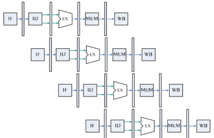
2.2. Five-stages pipeline
Pipelining is an implementation technique in witch multiple instructions are overlapped in execution. It can increase CPU throughput, MIPS instruction classically take five pipelining stage
1. IF(instruction fetch): fetch instruction from memory
2. ID(instruction decode): read registers while decoding the instruction.
3. EX(execution): Execute the operation or calculate an address
4. MEM(memory access): Access an operand in data memory
5. WB(write back): write the result into register file
The traditional five-stage pipelined MIPS show in Figure 1.
2.3. Pipeline hazard
Pipeline hazard means that the situation in pipeline when next instruction cannot execute in the following clock cycle, and there are three different types
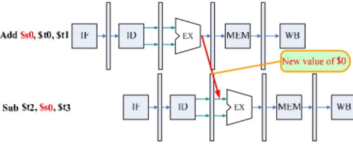
1. Structural hazard: Structural hazard means that the hardware cannot concurrently support multiple instructions in the same clock cycle. MIPS make it easy for designer to avoid structural hazard, it include two memories (Harvard architecture) instead of single memory (von Neumann architecture). 2. Data hazard: Data hazard occur when the
pipeline must be stalled because one step must wait for another to complete. In five stage pipeline, data hazard arise from the dependence of one instruction on an earlier one that still in the pipeline, and earlier instruction not in write back stage. The example shown as follow
add $S0, $S1, $S2; sub $S3, $S0, $S4;
The solution is data forwarding. In previous example, as soon as the ALU creates the sum for the add instruction, datapath can provide it as an input for the sub instruction.
3. Control hazard: Control hazard arising from the need to make a decision based on the result of one instruction while others are executing. The hardware solution is stall and predict
A. Stall: when branch occur, stall followed instruction until control unit make decision, but it is slow.
B. Predict: It means that apply a method to predict decision result. This option does not slow down the pipeline when predict correct, when predict wrong, you need rollback data and redo instructions.
III. MIPS32 Architecture Implementation
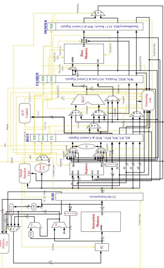
In this section, we focus on architecture implementation based on traditional five stages pipeline-IF, ID, EX, MEM and WB stage that include overall pipeline datapath and components, finally is construct simulation model.
3.1. Five-stages Pipelined MIPS32 datapath
The overall Five-stage Pipelined MIPS32 datapath are shown in Figure 5. Following is stages datapath and components detail implement methods.
3.1.1. Instruction Fetch stage
The Instruction Fetch stage is where a program counter will pull the next instruction from the correct location in instruction memory. These stages major functionalities are decide next instruction address and load instruction from instruction memory. The main components are program counter, instruction memory and branch prediction unit of this stage.
[1] Program Counter(PC)
A four bytes register to record next instruction address.
[2] Instruction Memory
The instruction memory was sized at 1k bits, total contains 32 separate instructions.
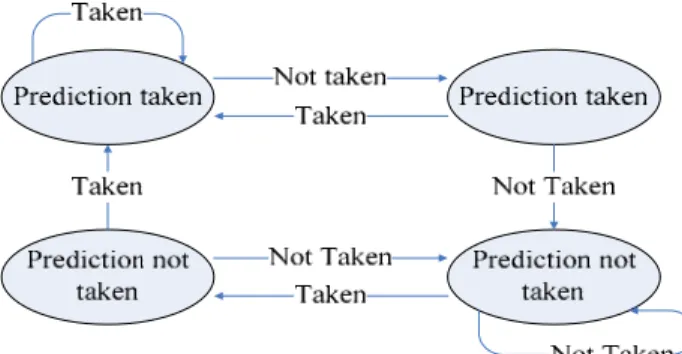
[3] Branch Prediction Unit
In order to reduce control hazard penalty, we choosing 2 bits history branch prediction mechanism, this mechanism key idea is unchanged prediction until predict wrong twice, the mechanism flow shown as Figure 6.
Figure 2. A Data Forwarding Example
Figure 3. A Stall Example
3.1.2. Instruction Decode stage
The Decode Stage is where the fetched instruction to decoding, load operator values from the register file and detect hazard. The main components are register file, control unit and hazard detect unit of this stage.
[1] Register File
The register file was sized at 1k bits, total contains 32 operator values.
[2] Control Unit
The Control unit takes the given Opcode and translate to control signal, these control signal control the MIPS32 datapath.
[3] Hazard Detect Unit
The hazard detection unit monitors output from the execute stage and memory stage to determine hazard conditions, these condition signal will control datapath to solve hazard.
3.1.3. Execution stage
The execute stage is responsible for taking the operator value and performing the specified operation. The forwarding unit forward data from datapath to avoid data hazard. The main components are arithmetic logical unit, multi-cycle multiplier, multi-cycle divider, barrel shifter and forwarding unit of this stage.
[1] Arithmetic Logical Unit
The arithmetic logical unit (ALU) is performing the calculations specified by the instruction. It takes two 32 bit inputs and some control signals, and gives a single 32 bit output,
The ALU functionality include add, sub, shift and compare. Detail functionality shown in Table 1. [2] Multi-Cycle Multiplier
(Booth’s Algorithm)
This is a signed multiplier that takes 32 cycles to calculate, Booth’s algorithm was invented by Andrew D. Booth in 1951, the hardware scheme shown as Figure 7.
[3] Restoring Multi-Cycle Divider
This is an unsigned divider that takes 32 cycles to calculate result, the hardware scheme shown as Figure 8.
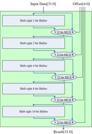
[4] Barrel Shifter
The barrel shifter [9] is a digital circuit that can shift a data word by a specified number of bits in one clock cycle, the hardware scheme shown as Figure 9.
Figure 7. Booth’s Algorithm Multiplier
Figure 8. Restoring Multi-Cycle Divider Figure 6. 2-Bits History Branch Prediction
[5] Forwarding Unit
The forwarding unit is responsible for choosing what input is to be fed into the ALU If register number conflict; this means that when an instruction tries to use a register in its execute stage or memory stage that an earlier instruction intends to write in its write back stage, we need forward data to ALU input instead of read data from register file.
[6] Forwarding Unit
The forwarding unit is responsible for choosing what input is to be fed into the ALU If register number conflict; this means that when an instruction tries to use a register in its execute stage or memory stage that an earlier instruction intends to write in its write back stage, we need forward data to ALU input instead of read data from register file.
3.1.4. Memory stage
The Memory stage is responsible for taking the output of execution stage and load or store a data from data memory. The main component is data memory of this stage.
3.1.5. Write back stage.
The write back stage is responsible for writing the result to the register file back, the result generates from data memory or ALU. It has input control lines that tell it whether this instruction writes back or not. Write number will guide the result to proper register file location.
3.2. MIPS32 simulation model
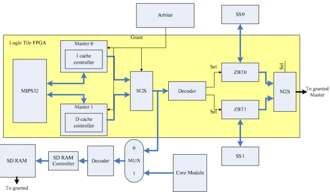
The basis of ARM integrator is difficult to debug, we map the ARM integrator hardware to soft IP, construct a pure software verification environment. The MIPS32 simulation model based on ARM integrator platform design, the hardware scheme shown as Figure 10
3.3. MIPS32 design flow
In this paper, we used several tools to implement MIPS32 hardware. Mentor Graphic Modelsim used to Simulation RTL design. Spring soft nLint used to check RTL coding style. Synopsys Design compiler used to logic synthesis. Synopsys Astro for physical synthesis. Detail design flow shown as Figure 11.
VI. Experiment results
This section contains MIPS32 functional verification and synthesis result.
4.1. RTL code Verification
In order to verify the MIPS32 simulation model, we choose DSPstone benchmark [7] as verification programs. DSPstone benchmark suite is based on algorithm kernels derived from important DSP applications. The benchmark experiment result shown in Table 2.
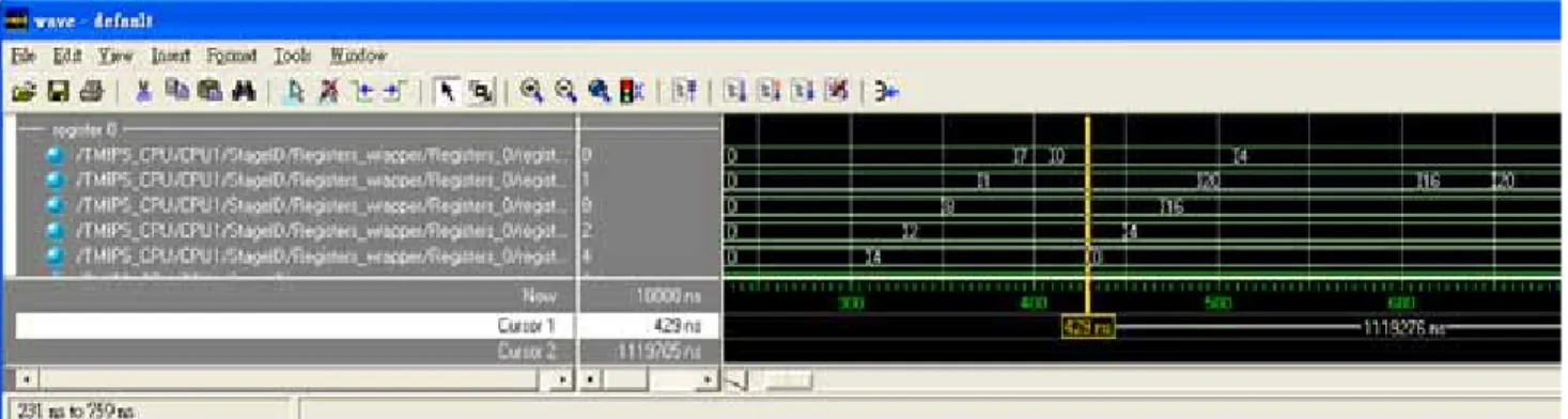
In Figure 12, we select a bubble sort assembly program as example. Original data is 4, 2, 8, 1, 7; the Shift right 1 bit Shifter
Shift right 2 bit Shifter
Shift right 8 bit Shifter Shift right 4 bit Shifter
Shift right 16 bit Shifter
1 32 bit MUX0
1 32 bit MUX0
1 32 bit MUX0
1 32 bit MUX0
1 32 bit MUX0
Input Data[31:0] Offset[4:0]
Result[31:0] Figure 9. Barrel Shifter
sorted result is 1, 2, 4, 7, 8, the waveform shown as Figure 13.
4.2. RTL code Synthesis
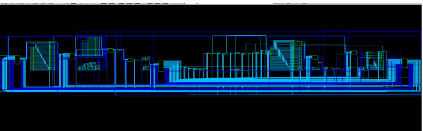
We choose Synopsys Design compiler as logic synthesis tool to synthesis MIPS32 RTL design, Figure 14 shows the symbol view and Figure 15 shows the schematic view.
Logic synthesis clock period set to 8.18ns, and met all design constraints. Working frequency up to 124.24 MHz. Total cells area is 9795118.40nm2, major module hierarchy area report shown in Table 3, and Synopsys Astro chip layout shown in Figure 16.
V. Conclusions
In this paper we provide a five-stage pipelined MIPS32 processor with corresponding design flow. The proposed processor implements complete eighty integer instructions of MIPS32 instruction set architecture. To verify this design, we develop two levels of verification environments: functional verification on proposed Simulation Model with Verilog Simulator and FPGA proven on ARM Integrator with FPGA implemented on attached Logic Tile. .Finally we adopt Synopsys Design Compiler to synthesize our MIPS32 processor by TSMC 0.13µm technology. The result proves the work frequency of our design can achieve 124.24
MHz. The chip layout generated by Synopsys Astro is also provided.
VI. Reference
[1] ARM Inc., “AMBA Specification Rev.2.0.”. [2] ARM Inc., “INTEGRATOR ® / CM920T,
CM920T-ETM, CM940T CORE MODULE USER GUIDE”.
[3] ARM Inc., “INTEGRATOR ® / LT-XC2V4000 + LOGIC TILE USER GUIDE”.
[4] ARM Inc., “INTEGRATOR TM / AP ASIC PLAFORM USER GUIDE”.
[5] D. A. Patterson and J. L. Hennessy, ”Computer Organization and Design The Hardware/Software Interface Third Edition”, Morgan Kaufmann, 2007.
[6] D A. Patterson and J. L. Hennessy, ”Computer Architecture A quantitative Approach Fourth Edition”, Morgan Kaufmann., 2007.
[7] H. Meyr, ”DSP Compiler and Processor Evaluation - DSPstone”, [Online]. Available:
http://www.iss.rwth-aachen.de/Projekte/Tools/DSPSTONE/dspstone. html. [Accessed: July 9, 2009].
[8] MIPS Technologies Inc., ”MIPS32 Architecture For Programmers Architecture Revision 2.00”, 2003.
[9] P. Gigliotti, ”Implementing Barrel Shifters Using Multiplexer”,2004
Sel
Figure 10. Proposed MIPS32 Simulation Model
Basic MIPS32 RTL Coding
Syntax Check by nLint Verification by
Modelsim
MIPS32 Simulation Model RTL Coding
Syntax Check by nLint Verification by Modelsim Logic Synthesis by Design Compiler Physical Synthesis by Astro
Verification & Syntax Pass?
Verification & Syntax Pass?
No
Yes
No
Yes
Gate level netlist
GDS II
Figure 13. Sorted Data Waveform View Figure 12. Unsorted Data Waveform View
Figure 15. Design Compiler Schematic View
Operation Action
ANDU Unsigned add
OR Logical or
ADD Signed add
CLO Counting 1
CLZ Counting 0
SLLV Logical Shift left, shift amount is GPR[4..0]
SRLV Logical shift right, shift amount is GPR[4..0]
SRL Logical shift right, shift amount is Instruction[10..6]
SRA Arithmetical shift right, shift amount is Instruction[10..6]
SLL Logical shift left, shift amount is Instruction[10..6]
SRAV Arithmetical shift right, shift amount is GPR[Rs]4..0
MOVN Move conditional on not zero
MOVZ Move conditional on zero
SUBU Unsigned subtract
SUB Signed subtract
SLTU If (unsigned(GPR[Rs])>unsigned(GPR[Rt])) ALUout =1; Else Aluout =0; SLT If (signed(GPR[Rs])> signed(GPR[Rt])) ALUout =1; Else ALUout =0;
SEB Sign Extend Byte
SHE Sign Extend Halfword
WSBH Word Swap Byte Halfword
XOR Exclusive OR
NOR Bitwise logical NOT OR
DSPstone Benchmark Program Name Execution Cycle Counts mat1x3 124901 complex_multiply 57052 biquad_one_section 83110 biquad_N_sections 119724 real_update 17853 n_real_updates 182738 fir 324500 fir2dim 1791852 complex_update 49577 n_complex_updates 682616 lms 370839 convolution 249187 dot_product 27430
Table 2. The Verified DSPstone Programs and their Execution Cycle Counts
Hierarchical cell Combinational Non-combinational Total
MIPS_CPU 1646.4757 334.3878 1015255.3125 CP0 31895.3125 70564.9141 104694.617 StageDM 3617.1609 0 4941.1362 StageEX 4616.9326 0 164255.1562 StageEX/ALU 13411.1572 0 106695.7031 StageEX/ALU/Shifter 5625.1909 0 77928.4453 StageEX/ALUcontrol 3352.3674 0 3352.3674 StageEX/ForwardUnit 2133.6326 0 2133.6326 StageEX/div_wrapper/divide 5413.0396 5572.5562 19351.8691 StageEX/mult_wrapper/multiplier 2167.5784 4430.2124 12881.5557 StageID 9337.4004 0 477904.7812 StageID/Control 2053.8545 0 2053.8545 StageID/hazard_detection 339.4800 0 339.4800 StageIF 3457.6050 0 14611.2031 StageIF/PC 1130.4683 1856.9550 2987.4243 StageIF/predictor 818.1467 81.4752 3352.3672 Total 650912.1250 4334.5312 1015253.964666