複晶矽之藍光飛秒雷射退火
102
0
0
全文
(2) 複晶矽之藍光飛秒雷射退火 Blue Femtosecond Laser-Induced Crystallization of Amorphous Silicon. 研 究 生: 陳冠文. Student: Kuan-Wen Chen. 指導老師: 潘犀靈 教授. Advisor: Prof. Ci-Ling Pan. 國立交通大學 光電工程研究所 碩士論文. A Thesis Submitted to Department of Photonics & Institute of Electro-Optical Engineering College of Electrical Engineering National Chiao Tung University In partial Fulfillment of the Requirements for the Degree of Master of Engineering In Electro-Optical Engineering. July 2005 Hsinchu, Taiwan, Republic of China. 中 華 民 國 九 十 四 年 七 月.
(3) 複晶矽之藍光飛秒雷射退火. 研究生:陳冠文. 指導老師:潘犀靈 教授. 國立交通大學光電工程研究所. 摘要. 我們利用鈦藍寶石超快雷射倍頻(λ = 400 nm)藉由掃描的方式對 非晶矽進行藍光飛秒雷射退火結晶。由於超短脈衝雷射導致材料的非 線性吸收效應在材料表面產生緻密的電漿,使得非晶矽發生非線性熔 融。我們對藍光飛秒非晶矽晶退火再結晶形成複晶矽結構之最佳條件 及樣品特性加以探討。 從實驗結果,我們發現在當達到是當能量密度條件下,複晶矽在 脈衝重疊百分比達 89.8%以上時會開始成長。當我們繼續增加脈衝重 疊百分比時,將會有更多的能量被非晶矽所吸收,並激發價帶電子躍 遷至導帶,這過程使得經藍光飛秒雷射退火之非晶矽轉變成為複晶 矽,當我脈衝重疊百分比增加到臨界時,晶粒便開始遞減。 從實驗結果可觀察到,在室溫下儘管我們提高脈衝重疊百分比, 晶粒的成長大小似乎有一個極限值存在,由實驗結果可知:在室溫 I.
(4) 時,最大平均晶粒約 280 nm,此時所用能量密度為 30 mJ/cm2,93.75% 的脈衝重疊百分比。 最後我們從光子吸收係數與光穿透深度的觀點,將藍光飛秒雷射 退火與近紅外飛秒雷射退火和準分子雷射退火加以比較、討論。. II.
(5) Blue Femtosecond Laser-Induced Crystallization of Amorphous Silicon Student: Kuan-Wen Chen. Advisor: Prof. Ci-Ling Pan. Institute of Electro-Optical Engineering Department of Photonics College of Electrical Engineering Science National Chiao Tung University Abstract Amorphous silicon (a-Si) was crystallized by femtosecond laser annealing (FLA) using a blue (λ= 400 nm) ultrafast Ti:Sapphire laser system. The line-scan method was applied in the experiment. The intense ultrashort laser pulses lead to efficient nonlinear absorption and the generation of very dense photoexcited plasma in irradiated materials, enabling nonlinear melting on silicon materials. We also study the structural characteristics of recrystallized amorphous silicon films. The grains in the FLA-processed a-Si were found to grow larger as overlapping between irradiated areas was increased up to 89.8% at appropriate fluence. When we increase the overlapping at the same fluence, there will be more energy absorbed by amorphous silicon layer to excite the electrons from valence band to conduction band. Then the annealed amorphous silicon translates into polycrystalline silicon. After increasing the overlapping larger the threshold, the grain size decrease oppositely. III.
(6) We observe that there seems to be a grain size limitation in the room temperature condition even though we increase the overlapping condition. We get the largest grain size is around 280 nm as fluence is 30 mJ/cm2 and overlapping is 93.75% at room temperature. At last we make comparisons with near-infrared femtosecond laser annealing and excimer laser annealing from the viewpoints of absorption coefficient and penetration depth.. IV.
(7)
(8) Acknowledgement (誌謝) 「沒有岸邊的礁石,又怎能激起美麗的浪花」…在研究的大道上,首 先我要由衷地感謝 潘犀靈教授不僅在研究精神與方法的啟發,且在專業 知識的教導與實驗結果的討論皆使我獲益良多,還有孫啟光教授、趙如蘋 教授與林恭如教授對論文的批評與指正,猶如醍醐灌頂。 回想碩班生涯,我想特別感謝王怡超學長在實驗系統與論文架構上的 幫忙、李晁奎學長與陳晉瑋學長在問題的指點及生活所賦予的歡樂回憶、 與劉子安學長與藍玉屏學姐在其專業領域的討論,陳尊豪先生辛苦地量測 實驗結果、以及謝卓凡學長和許乃今學妹為實驗室注入活力泉源。 最特別的是有七位互相砥礪的好同學,黃照仁、吳宗翰、莊沁融、陳 弘倫、羅誠、高禎祐與吳勝隆,生活的協助、知識的交流與同甘共苦的精 神都將深刻的留在腦海,點點滴滴,都是我們共同的美好回憶,願未來的 日子,能更上一層樓,創造出屬於自己的天地。 最後我要向爸爸、媽媽致上最高的敬意,有你們的大力栽培,才有今 日的我,還有大姐、二姐和雅穎,你們的支持與鼓勵,是我源源不絕的動 力。. 2005 年 7 月 于 風城 交大. V.
(9) Contents Page. Chinese Abstract………………………………………………I English Abstract……………………………………………III Acknowledgement………………………………………….....V Contents………………………………………………………VI Table & Figure Captions…………………………………..VIII. Chapter 1 Introduction……………………………….………1 1.1 Basic Concept of TFT-LCD ………………………………………… 1 1.1.1 History of TFT-LCD ………………………………………….. 1 1.1.2 Principle of LCD Technology.………………………………… 4 1.2 Motivation and Objective…………………………………………...11 1.3 Organization of this thesis…………………………………………..13. Chapter 2 Preparation and Properties of Low Temperature Poly-Silicon……………………………………………...……15 2.1 Introduction of Low Temperature Poly-Silicon………………….15 2.2 Preparation of Poly-Silicon……………………………………….21 2.2.1 Solid Phase Crystallization......................…………..……….21 2.2.2 Excimer Laser Annealing…………………………….………24 2.2.3 Femtosecond Laser Annealing……………………….………32 VI.
(10) Chapter 3 Experimental Methods……………………..……36 3.1 Sample Preparation…………………………………………………36 3.2 The Blue Femtosecond Laser System……………………………..38 3.2.1 Introduction to Femtosecond Laser System………………...38 3.2.2 Characterization of Blue Femtosecond Laser Pulse…………42 3.3 The Laser Annealing station………………………………………..45 3.4 Characterization of Annealing Samples……………………………47. Chapter 4 Results and Discussions………………….………63 4.1 Comparisons with Near-infrared Femtosecond Laser Annealing….63 4.2 Comparisons with Excimer Laser Annealing……………………….70. Chapter 5 Conclusions……………………………….………75 5.1 Summary…………………………………………………………75 5.2 Future work………………………………………………………77. Reference………………………………………………..……78. VII.
(11) Table Captions Table 2-1: Main laser lines of several common excimer lasers. Table 3-1: Spectra Physics Tsunami specifications. Table 3-2: The specifications of the regenerative amplifier. Table 3-3: Chemical and structural properties of BBO crystal [43]. Table 3-4: Optical and nonlinear optical properties of BBO crystal [43].. VIII.
(12) Figure Captions Fig. 1-1: Liquid crystal works by applying voltage. Fig. 1-2: LCD panel produces colors by adjusting the proportion of the 3 color pixels. Fig. 1-3: TFT-LCD has a sandwich-like structure. Fig. 1-4: (a) Structure of passive matrix drive system [3]. (b) Circuitry of passive matrix drive system [3]. Fig. 1-5: (a) structure of active matrix drive systems [3]. (b) Circuitry of active matrix drive systems [3]. Fig. 1-6:. A schematic diagram of TFT-LCD array with controllers, power supply, and driver circuits shows the driving of an LCD panel.. Fig. 2-1: The crystal structure and electrical characteristics performance comparison between the silicon thin films. Fig. 2-2: Concepts of circuit integration. The comparisons of a-Si TFT-LCD, poly-Si TFT-LCD, and poly-Si TFT-LCD system on panel (SOP). Fig. 2-3: The difference of aperture ratio between a-Si TFT and poly-Si TFT [23].. IX.
(13) Fig. 2-4:. Schematic of a typical solid phase crystallization (SPC) system. The system consists of a quartz tube with cantilever inside to support the cassettes with wafers, exhaust system, gas control system, and temperature control system.. Fig. 2-5: Schematic of a typical excimer laser annealing (ELA) system. It is used for LTPS of large size LCD substrate manufacture. This ELA system includes Laser head, optical path, homogenizer, annealing chamber, and transfer controller [31]. Fig. 2-6: Principle of excimer laser annealing. The pulsed excimer laser beam is homogenized and shaped to a line and scanned across the surface. Within the laser pulse duration the amorphous silicon layer is rapidly heated and melted. As it cools down the recrystallization into polycrystalline silicon occurs. Fig. 2-7:. Three regimes of ELA includes partial melting, nearly complete melting and complete melting. The nearly complete melting between the other two regimes is also called super lateral growth (SLG) of excimer laser annealing (ELA).. Fig. 2-8: Comparison of SLG and C-SLG modes of growth. In SLG (left panels) growth initiates from seeds, which survived the melting process, at the Si-SiO2 interface. In C-SLG (right panels) the poly-Si microstructure forms by lateral epitaxy from seeds generated at the liquid-solid interface. Notice the difference in the width of the molten zone between SLG and C-SLG.. X.
(14) Fig. 2-9:. Timescales of various electron and lattice processes in laser-excited. solids.. Each. green. bar. represents. an. approximate range of characteristic times over a range of carrier densities from 1017 to 1022 cm–3. The triangles at the top show the current state-of-the-art in the generation of short pulses of electromagnetic radiation: 1 5 fs (visible), 2 120 fs (X-ray), 3 0.5 fs (far ultraviolet) [15,39]. Fig. 3-1: Schematic description of LPCVD device. Fig. 3-2: Femtosecond laser system includes Tsunami, Spitfire, and two pump laser (Millennia V and Evolution X). Fig. 3-3: Tsunami femtosecond cavity layout [42]. Fig. 3-4: The Spitfire amplification process. Fig. 3-5: The frequency doubling setup in the experiments. Fig. 3-6: The frequency doubling power transformation ratio. Fig. 3-7:. Schematic diagram of blue femtosecond laser annealing experiment setup.. Fig. 3-8: Our femtosecond laser annealing chamber and transition stage. (a) Blue femtosecond laser annealing setup – vacuum chamber. (b) Blue femtosecond laser annealing setup –XY transition stage. Fig. 3-9:. Average grain seize versus overlapping at 20.0 mJ/cm2.. Fig. 3-10: Average grain seize versus overlapping at 21.7 mJ/cm2. Fig. 3-11: Average grain seize versus overlapping at 23.3 mJ/cm2. Fig. 3-12: Average grain seize versus overlapping at 25.0 mJ/cm2. XI.
(15) Fig. 3-13: Average grain seize versus overlapping at 26.7 mJ/cm2. Fig. 3-14: Average grain seize versus overlapping at 28.3 mJ/cm2. Fig. 3-15: Average grain seize versus overlapping at 30.0 mJ/cm2. Fig. 3-16: Average grain seize versus overlapping as the flunce changes. Fig. 3-17: Average grain seize versus fluence as 85.00% overlapping. Fig. 3-18: Average grain seize versus fluence as 87.50% overlapping. Fig. 3-19: Average grain seize versus fluence as 90.00% overlapping. Fig. 3-20: Average grain seize versus fluence as 92.50% overlapping. Fig. 3-21: Average grain seize versus fluence as 93.75% overlapping. Fig. 3-22: Average grain seize versus fluence as 95.00% overlapping. Fig. 3-23: Average grain seize versus fluence as 96.25% overlapping. Fig. 3-24: Average grain seize versus fluence as 97.50% overlapping. Fig. 3-25: Average grain seize versus overlapping as the flunce changes. Fig. 3-26: This sample was produced as fluence is 30 mJ/cm2 and overlapping is 93.75% at room temperature. The sharp peak centered at ~ 519.5 cm-1. The FWHM is ~ 7.5 cm-1. Fig. 3-28: (a), (b), and (c) are AFM images of blue FLA poly-Si films irradiated with 50 fs pulses. (a) fluence of 28.3mJ/cm2 and an interpulse overlapping of 90.0%. (b) fluence of 28.3mJ/cm2 and an interpulse overlapping of 92.5%. (c) fluence of 28.3mJ/cm2 and an interpulse overlapping of 96.25% Fig. 4-1: SEM images of FLA poly-silicon samples after Secco etching for steady-state (a), (b), (c), (d) and scanned FLA (e), (f), (g), (h) [21].. XII.
(16) Fig. 4-2: (a) Average grain sizes of FLA poly-silicon films, irradiated with pulses of different durations, as a function of laser fluence for steady-state FLA and scanned FLA [21]. (b) Average grain sizes of FLA poly-silicon films, irradiated with pulses of different durations, as a function of overlapping for steady-state FLA and scanned FLA [21]. Fig. 4-4: (a) The profile of near-infrared femtosecond laser annealing sample at 400°C and 45mJ/cm2. (b) The profile of blue femtosecond laser annealing sample at 100°C and 23.3mJ/cm2. Fig. 4-3: (a) Optical properties of 0.5 –1.5 µm-thick samples of a-Si:H. These results were obtained at room temperature by combining dual beam photoconductivity spectroscopy, transmittance. and. reflectance. spectroscopy,. and. spectroscopic ellipsometry measurements [44]. (b) Absorption coefficient of amorphous and microcrystalline silicon films grown by ECR-CVD (in the same figure the absorption coefficient of monocrystalline silicon is reported [45]. (c) Subgap absorption spectra showing the absorption coefficient (after interference corrections) for a-Si:H thin films with a thickness of 4 nm ( ), 9 nm ( ), 30 nm ( and 98 nm ( ) [46].. XIII. ),.
(17) Fig. 4-4: (a) The profile of near-infrared femtosecond laser annealing sample at 400 °C and 45 mJ/cm2. (b) The profile of blue femtosecond laser annealing sample at 100 °C and 23.3 mJ/cm2. Fig. 4-5: A series of images zoom in from initial samples. (a) Annealed silicon wafer. (b) poly-silicon on the wafer annealed at 28.3 mJ/cm2; 93.75%. (c) SEM images of the area in (b). (d) poly-silicon on the wafer annealed at 30.0 mJ/cm2; 97.50%. (e) SEM images of the area in (d). (f) SEM images of the area in (e).. XIV.
(18) Chapter 1 Introduction In chapter 1 of this thesis, an overview of TFT-LCD technology is presented first. History of TFT-LCD and principles of LCD technology would be introduced in section §1.1. Then the motivation and objective of the thesis would be written in section §1.2. In section §1.3, an organization of this thesis is given in detail.. 1.1 Overview of TFT-LCD Technology 1.1.1 History of TFT-LCD Liquid crystals were discovered by the Austrian botanist Rheinitzer in 1888. Liquid crystal is a term that indicates the status of a substance that is neither solid nor liquid, e.g. soapy water. In 1963, Williams, while working for RCA discovered that the way light passes through liquid crystal changes when it is stimulated by an electrical charge. Five years later, another RCA researcher named Heilmeyer and his colleagues made a display prototype that applied this concept. This prototype's success marked the beginning of modern liquid crystal display (LCD) technology. In the beginning, liquid crystals were initially too unstable to use as a material for manufacturing display units, resulting in several market problems for LCD technology until a professor of the University of Hull in the U.K. discovered a stable liquid crystal material (biphenyl).. 1.
(19) In recent years, the growth of flat panel displays in many fields is apparent. The flat panel displays includes liquid crystal display (LCD), light emitting diode (LED), electroluminescent (EL) panel, vacuum fluorescent display (VFD), and plasma display (PDP). Liquid crystal displays (LCDs) are the most popular among the various flat panel displays. Of all these systems, the liquid crystal display is considered to be the most promising. In addition to being thin and lightweight, these displays run on voltages so low they can be driven directly by a Large Scale Integrated Circuit (LSI). Since LCDs consume low power, they can run for long periods on batteries. However, limited viewing angle characteristics, large response times and limitations in the electro-optic characteristics were some of the drawbacks of LCD for large information content displays like video displays and televisions. Many researchers and engineers have been engaged in improving the characteristics of liquid crystal displays since that time. The first AMLCD was successfully demonstrated by Brody in 1973, where a CdSe TFT was used as a switching element for each pixel of a 120 x 120 matrix [1]. After LeComber reported the first amorphous hydrogenated silicon (a-Si:H) TFT [2], many groups started the development of AMLCD using a-Si:H TFTs formed on glass substrate. Color filters were used in the transmission mode to realize the color displays. AMLCDs currently are mainly available on the market which use a-Si:H TFTs and polycrystalline silicon (poly-Si) TFTs. There are two trends in the development of TFT-LCD. One is the direct-view displays for use in notebooks and televisions, where LCD 2.
(20) with larger screen sizes and higher pixel-content are required. The other is toward compact LCD modules with high pixel density for use in cell phones, projection television sets and digital cameras as monitor display. Amorphous hydrogenated silicon (a-Si:H) TFT-LCDs have been widely used for many applications in direct view displays such as notebooks, televisions, personal computers, and various monitors. LCD screen size has rapidly increased during the last 10 years. Small-size LCDs with high pixel densities are also used as light valves for LCD projectors and viewfinders for digital cameras. Poly-Si TFTs are suitable for such applications since the monolithic drivers around the screen preclude a limit on connector pitches between driver ICs and display signal lines. Because LCD has unique and superior features such as compactness, thin, light and low-power consumption in principle, it is a promising technology for realizing high quality interface such as displays, projectors, and portable personal devices.. 3.
(21) 1.1.2 Principles of LCD Technology Light passes through liquid crystals, following the direction in which the molecules are arranged. When the molecule arrangement is twisted 90 degrees as shown in Fig. 1-1, the light also twists 90 degrees as it passes through the liquid crystals. The molecules in liquid crystals are easily rearranged by applying voltage. When voltage is applied, molecules rearrange themselves along with the electric field vertically and light passes straight through along the arrangement of molecules. A combination of polarizing filters and twisted liquid crystal creates a liquid crystal display. When two polarizing filters (polarizers) are arranged along perpendicular polarizing axes, light entering from below is re-directed 90 degrees along the helix arrangement of the liquid crystal molecules so that it passes through the upper polarizer. The liquid crystal molecules straighten out and stop redirecting the angle of the light as voltage is applied. Therefore, no lights can pass through that area of the LCD and it makes that area darker than the surrounding areas. The color filter of a TFT-LCD consists of three primary colors (Red, Green, and Blue).. The elements of this color filter line up. one-to-one within the unit pixels on the TFT-array substrate. Each pixel is divided into three subpixels, where one set of RGB subpixels is equal to one pixel. Because the subpixels are too small to distinguish separately, the RGB elements seem to the human eye as a mixture of the three colors. It will produce lots of colors by mixing these three primary colors (RGB) (see Fig. 1-2). 4.
(22) Polarizer Color Filter Liquid Crystal. AC Voltage. TFT Polarizer Backlight Fig. 1-1: Liquid crystal works by applying voltage.. Polarizer Color Filter. Liquid Crystal TFT Polarizer Backlight. Fig. 1-2: LCD panel produces colors by adjusting the proportion of the 3 color pixels. 5.
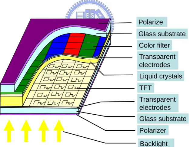
(23) Today's TFT-LCD has a sandwich-like structure (see Fig. 1-3). It consists of liquid crystal, two polarizers and glass substrates. The top substrate is color filter, the bottom substrate is TFT array. Two Polarizers control the light entering and leaving. Glass substrate stops the filtering of electricity from electrodes. Color is expressed through the use of R, G and B color filters. Transparent electrodes drive the TFT-LCD. A highly transparent material (ITO) is used that will not interfere with the quality of the image's integrity. Liquid crystal material is injected between two glass plates. TFT array control the liquid crystal direction by applying voltage. The display operates in the transmission mode with fluorescent lamp behind the panel.. Polarize Glass substrate Color filter Transparent electrodes Liquid crystals TFT Transparent electrodes Glass substrate Polarizer Backlight Fig. 1-3: TFT-LCD has a sandwich-like structure.. 6.
(24) The driving method of LCD is dividing roughly into passive matrix LCD and active matrix LCD.. Passive Matrix LCD (PMLCD) In this method, the transparent electrodes are set on X and Y electrodes as shown in Fig. 1-4(a). There are no switching devices in passive matrix LCD (PMLCD) as shown in Fig. 1-4(b), and each pixel is addressed for more than one frame time. Because all electrodes are electrically connected together, the effective applied voltage must average the signal voltage pulses over several frame times. Therefore, this driving method results in a slow response time and a reduction of the maximum contrast ratio. The addressing of a PMLCD also produces a kind of crosstalk that produces fuzzy images because non-selected pixels are driven through a secondary signal-voltage path. Passive matrix LCDs are used in watches, calculators, or cheap hand held video games. As the pixel density (resolution) increased, however, passive matrix technology was no longer suitable as crosstalk became an issue with displays larger than 100×100 pixels.. Active Matrix LCD (AMLCD) The configuration of a typical AMLCD is shown in Fig. 1-5(a). The pixels are arranged in X-Y matrix formed on the bottom glass substrate as shown in Fig. 1-5(b). 7.
(25) (b) Circuitry. (a) Structure. Fig. 1-4: (a) Structure of passive matrix drive system [3]. (b) Circuitry of passive matrix drive system [3].. (b) Circuitry. (a) Structure. Fig. 1-5: (a) structure of active matrix drive systems [3]. (b) Circuitry of active matrix drive systems [3].. 8.
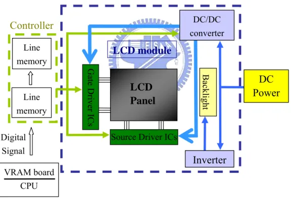
(26) Each pixel has an a-Si:H TFT which operates as an analogue switch to control the stored charge in an LC capacitor. The capacitance is defined between the pixel electrode on the bottom substrate and a common electrode on the top substrate. Active-pixel technology was invented so that the voltage applied at each pixel was well isolated from the other pixels [4]. The TFT made a suitable low-conductivity switch as turned off, had sufficient conductivity in the on-state such that it could charge a liquid crystal pixel's capacitance, and polarize the liquid crystal.. DC/DC converter. Controller Line memory. LCD Panel. Backlight. Gate Driver ICs. Line memory. LCD module DC Power. Source Driver ICs. Digital Signal. Inverter. VRAM board CPU. Fig. 1-6: A schematic diagram of TFT-LCD array with controllers, power supply, and driver circuits shows the driving of an LCD panel.. 9.
(27) Fig. 1-6 is a schematic diagram of the TFT-LCD array with controllers, a power supply, and other driver circuits shows the driving of an LCD panel. The TFT substrate consists of a TFT array and an array of external terminals on which large-scale integrations (LSIs) are bonded to drive the TFT panel. These LSIs are directly bonded to the glass with tape automated bonding (TAB) connectors, and they provide each pixel of the panel with video signals to drive the LCD panel.. 10.
(28) 1.2 Motivation and Objective Hydrogenated amorphous silicon (a-Si:H) is used extensively in Thin Film Transistors (TFTs) for Flat Panel Displays (FPDs) and large area imagers, and it is also a promising photovoltaic material. a-Si:H TFTs have a low off-current and sufficient on-current for most applications. However, a-Si:H has poor carrier mobility. The low mobility of a-Si:H results in a limitation on pixel sizes for display and imaging applications. Poly-Si has been proposed as an alternative to a-Si:H, as it can have mobility of up to 300 cm2 V-1 s-1. High performance silicon devices on insulators have recently been incorporated in various applications, such as lightweight flat panel displays. The key for realizing such systems (SOP) is low temperature polycrystalline silicon (LTPS) TFT. Low-thermal-budget techniques, such as plasma-assisted hydrogen-[5], metal-[6], and laser-induced crystallization [7-14] are commonly employed to LTPS as the channel regions. In particular, efficient absorption of ultraviolet (UV) laser irradiation by hydrogenated amorphous silicon (a-Si:H) results in high-quality polycrystalline silicon (poly-Si) by excimer laser annealing (ELA) [9-11]. Unlike annealing using continuous-wave [14] and long pulse lasers (tens ns range), nonlinear photon absorption and nonequilibrium thermodynamics are expected to dominate the interactions by the femtosecond laser pulses [15-20]. Such a nonlinear process provides precise and low fluence associated with femtosecond laser ablation [17-20]. Our group had presented a near-infrared femtosecond laser (λ = 11.
(29) 800 nm) annealing with 50 fs pulse duration [21]. In order to investigate the femtosecond laser-induced crystallization of amorphous silicon further, we utilize blue femtosecond laser (λ = 400 nm) to do annealing experiment in this thesis. Then we study the structural characteristics of recrystallized amorphous silicon films. At last we make comparisons with near-infrared femtosecond laser annealing and excimer laser annealing. We report blue femtosecond laser-induced crystallization of amorphous silicon with high crystallinity, using ultralow laser energy.. 12.
(30) 1.3 Organization of this thesis In chapter 1 of this thesis, an overview of TFT-LCD technology is presented first. History of TFT-LCD and principles of LCD technology would be introduced in section §1.1. Then the motivation and objective of the thesis would be written in section §1.2. In the beginning of chapter 2, low temperature poly-silicon (LTPS) is given in detail. In section §2.2, several recrystallization methods which include solid phase crystallization (SPC), excimer laser annealing (ELA), and femtosecond laser annealing (FLA) are introduced. In chapter 3, our sample preparation is mentioned. After that, a brief introduction to our femtosecond laser pulse and the frequency doubling process separately are described. Then we could see the experimental components completely in the schematic diagram of experiment setup in section §3.3. In section §3.4, the characterizations of blue femtosecond laser annealing samples which include scanning electron microscope (SEM) images and Raman spectra are presented finally. In chapter 4, our group’s near-infrared femtosecond laser annealing work is reviewed first. Comparisons between the differences of absorption coefficient and penetration depth of near-infrared femtosecond laser annealing and blue femtosecond laser annealing are discussed in section §4.1. Then, Comparisons between difference of mechanism of excimer laser annealing (ELA) and blue femtosecond laser annealing are reported in section §4.2. Finally in chapter 5, summary of the blue femtosecond laser 13.
(31) annealing would be written in section §5.1 and suggestions to the future work are also presented in section §5.2.. 14.
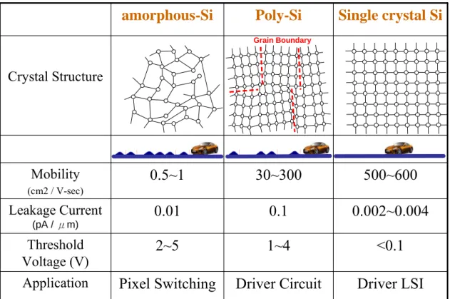
(32) Chapter 2 Properties and Preparation of Low Temperature Poly-Silicon In the beginning of chapter 2, low temperature poly-silicon (LTPS) is given in detail. In section §2.2, several recrystallization methods which include solid phase crystallization (SPC), excimer laser annealing (ELA), and femtosecond laser annealing (FLA) are introduced. 2.1 Introduction of Low Temperature Poly-Silicon Low temperature poly-silicon (LTPS) technology has been studied for more than a decade, for the purpose of driver integration at the periphery of AMLCD. With increasing the display area and pixel density of TFT-LCD, high mobility TFTs are required for pixel driver of TFT-LCD in order to shorten the charging time of pixel electrodes. However, it is very difficult because hydrogenated amorphous silicon (a-Si:H) has low mobility (0.5 - 1 cm2 V-1 s-1). The problem of the low carrier mobility for a-Si TFTs can be overcome easily by introducing poly-silicon film instead of a-Si as a channel layer of TFTs. The poly-Si is the most promising material for obtaining such high mobility TFTs for pixel drivers, moreover, the peripheral driver circuits can be integrated on the same substrate. Fig. 2-1 shows the crystal structure and electrical characteristics performance comparison between the silicon thin films. From the diagrams (Crystal Structure) in Fig. 2-1, we could understand 15.
(33) the difference between amorphous silicon, poly-silicon, and single crystal silicon. The amorphous silicon is the non-crystalline form of silicon. Silicon is normally bonded to four neighboring silicon atoms. This is also the case in amorphous silicon. However, it does not form a continuous crystalline lattice as in crystalline silicon. Some atoms may actually have dangling bonds, which occur when it does not bond to four neighboring atoms. Since not all the atoms are four-fold coordinated, amorphous silicon is said to be under-coordinated. These dangling bonds are defects in the continuous random network, which can be passivated by introducing hydrogen into the silicon. It then becomes hydrogenated amorphous silicon. Because of the low mobility of the amorphous silicon, it’s not suitable for fast switch. Another series of diagrams also shows the mobility relationship between the three kinds of silicon (a-Si, poly-Si, and single crystal Si). If there were many barriers on the road, we could not drive fast. On the contrary, we could drive fast on the flat way. It is the same with the electrons move in the three kinds of silicon. If the electrons need to pass through the grain boundaries within the active-channel region of a TFT, the mobility is low. That’s why the poly-silicon’s mobility is higher than amorphous silicon, but still lower than single crystal silicon. Although the mobility of single crystal silicon is the highest, the conventional process temperature to manufacture the single crystal silicon film is over 1000 °C. But the melting point of the glass is about 550 °C. That’s why we cannot employ the single crystal silicon in TFT-LCD process.. 16.
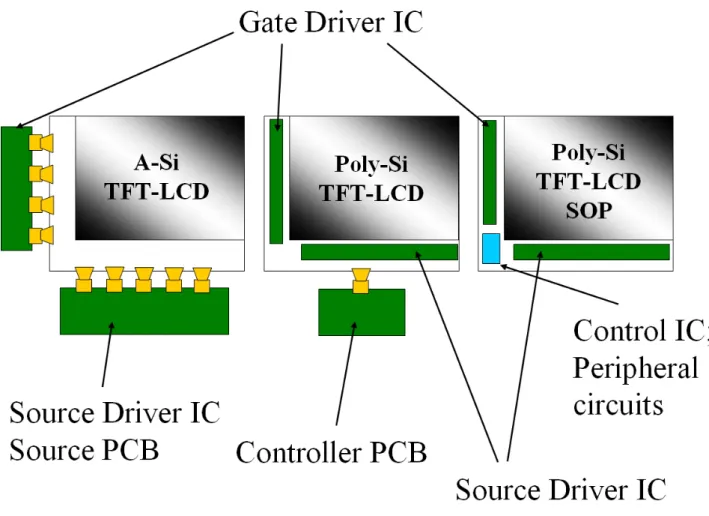
(34) amorphous-Si. Poly-Si. Single crystal Si. Grain Boundary. Crystal Structure. Mobility. 0.5~1. 30~300. 500~600. 0.01. 0.1. 0.002~0.004. Threshold Voltage (V). 2~5. 1~4. <0.1. Application. Pixel Switching. Driver Circuit. Driver LSI. (cm2 / V-sec). Leakage Current (pA / μm). Fig. 2-1: The crystal structure and electrical characteristics performance comparison between the silicon thin films. From Fig. 2-1, we know the leakage current of poly-Si is larger than a-Si:H. Many groups recently have studied the fabrication of high performance poly-Si TFTs with low leakage current, high mobility, high on/off current ratio, and good uniformity. In order to create the high quality TFT-LCD without flicker and cross-talk, we need to utilize poly-Si TFT with low leakage current (below 1 pA / µm) [24]. Fig. 2-2 shows the concept of circuit integration in TFT-LCD. As carrier mobility is improved, higher extent of integration will be possible. Low temperature poly-silicon allows integration of driver ICs onto the substrate. Both the number of external connections and the external size. 17.
(35) of the substrate could be minimized. System on panel (SOP) technology, implementing memories, sensors, and controllers with driver circuits of displays on glass, will be realized in the future with poly-Si thin-film transistors (TFTs) [22].. Fig. 2-2: Concepts of circuit integration. The comparisons of a-Si TFT-LCD, poly-Si TFT-LCD, and poly-Si TFT-LCD system on panel (SOP).. We could see another advantage of poly-silicon in Fig. 2-3. The transistor of LTPS LCD is smaller than that of amorphous-silicon. Thus,. 18.
(36) the aperture ratio of poly-silicon TFT-LCD and its screen brightness could be increased significantly [23].. Fig. 2-3: The difference of aperture ratio between a-Si TFT and poly-Si TFT [23]. The most conventional method to fabricate poly-Si is low pressure chemical vapor deposition (LPCVD) [24]. However, this method have some disadvantages such as high deposition temperature over 600°C, small grain size < 50 nm, poor crystallinity and high grain boundary states. Another disadvantage is the cheap glass substrate used in low temperature and large area processes could not be used in high temperature process. To enhance crystal properties, SPC is more useful method to increase the grain size than the as-deposited poly-Si film by LPCVD [25]. But it needs a long time annealing at high temperature over 600 °C. Now, there is a liquid phase recrystallization method such as ELA, which enable us to have good quality poly-Si film with large grain size and good electrical properties. ELA technology can be fabricate the 19.
(37) low temperature poly-Si TFT-LCDs without mechanical stress of glass substrate. Laser-induced crystallization is a promising process for obtaining a high quality poly-Si films [9-14]. But the excimer laser consists of toxic gas. People need to be careful as using excimer laser especially. Several recrystallization methods to produce poly-silicon would be explained in detail in the next paragraph which include solid phase crystallization (SPC), excimer laser annealing (ELA), and femtosecond laser annealing (FLA). 20.
(38) 2.2 Preparation of Poly-Silicon 2.2.1 Solid Phase Crystallization (SPC) Solid phase crystallization (SPC) of amorphous silicon attracted many interests for the application to poly-Si TFT-LCDs [29]. It is the most direct method of obtaining poly-Si films, from initially amorphous silicon films, is via SPC in furnace environment. Amorphous silicon is a thermodynamically metastable phase, processing a driving force for transformation to polycrystalline phase given sufficient energy to overcome the initial energy barrier. Unfortunately, SPC using low-temperature furnace annealing requires very long anneal times and hence suffers from a substantial tradeoff between performance and throughput [27].. The crystallization. from an amorphous phase to a polycrystalline phase occurs through two processes—nucleation and grain growth [27]. Both of them have characteristic activation energies. The nucleation activation energy is extracted from the time to onset of crystallization, while the grain growth rate is extracted from grain progression data. The nucleation activation energy is larger than the grain growth activation energy for the SPC system [28]. To achieve the largest possible grains, it is desirable to suppress nucleation relative to grain growth. Therefore, SPC is typically done at a low temperature. This results in a reduction in throughput through an increase in the incubation time and a decrease in the grain growth rate. Higher temperatures increase throughput oppositely. However, excessive nucleation results in smaller grains and hence poorer performance. 21.
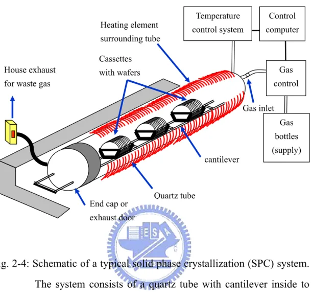
(39) Thus SPC can be accomplished within a wide annealing temperature range that requires a similar wide range of annealing time (i.e. time required for complete transformation of the precursor-Si film to poly-Si). The relationship between annealing temperature and annealing time is not unique. Based on the above transformation method, large grain size relates to longer crystallization time. For practical applications, the crystallization time corresponding to average grain size exceeding 0.5-1 µm may be prohibitingly long. The typical SPC poly-Si microstructure is characterized by a large density of structural defects. The result of this high grain-defect density is a saturation in the electrical performance of poly-Si TFTs, fabricated with such poly-Si films with grain size larger than approximately 0.3-0.5 µm. Therefore, standard SPC technology can only produce poly-Si TFTs of mediocre performance. This translated to a mobility range 20 - 40 cm2 V-1 s-1 and the threshold voltage ranges from 3 to 6 V [11]. Despite of the mediocre performance, solid phase crystallization (SPC) is a promising technique due to its simplicity, low cost, and excellent uniformity [29]. Fig. 2-4 shows a solid phase crystallization system. As it works, the amorphous silicon wafers would be placed in the cassette on the cantilever inside the quartz tube. Then the quartz tube would be heated by the surrounding elements. The temperature and gas inside the quartz tube were controlled by the computer systems.. 22.
(40) Heating element surrounding tube. Temperature. Control. control system. computer. Cassettes House exhaust. Gas. with wafers. control. for waste gas. Gas inlet Gas bottles cantilever. End cap or. (supply). Quartz tube. exhaust door. Fig. 2-4: Schematic of a typical solid phase crystallization (SPC) system. The system consists of a quartz tube with cantilever inside to support the cassettes with wafers, exhaust system, gas control system, and temperature control system.. 23.
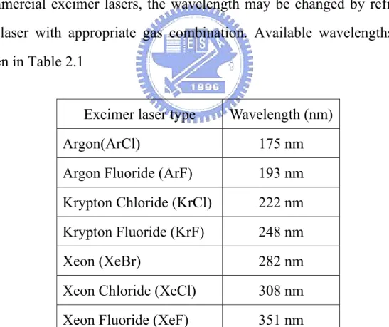
(41) 2.2.2 Excimer Laser Annealing (ELA) Excimer is acronym for “excited dimmer,” a molecule consisting of generally two atoms (for example, krypton and fluorine) which are strongly bound in the excited or upper energy level state and dissociate in the ground state; an excited complex of two molecules. Excimer lasers are a family of pulsed lasers operating in the ultraviolet region of the spectrum. The source of the emission is a fast electrical discharge in a high pressure mixture of a rare gas (krypton, argon, or oxygen) and a halogen gas (fluorine or hydrogen chloride). The particular combination of rare gas and halogen determines the output wavelength, and in most commercial excimer lasers, the wavelength may be changed by refilling the laser with appropriate gas combination. Available wavelengths are given in Table 2.1 Excimer laser type. Wavelength (nm). Argon(ArCl). 175 nm. Argon Fluoride (ArF). 193 nm. Krypton Chloride (KrCl). 222 nm. Krypton Fluoride (KrF). 248 nm. Xeon (XeBr). 282 nm. Xeon Chloride (XeCl). 308 nm. Xeon Fluoride (XeF). 351 nm. Table 2-1: Main laser lines of several common Excimer lasers.. For users with unique requirements for pulsed radiation in the 24.
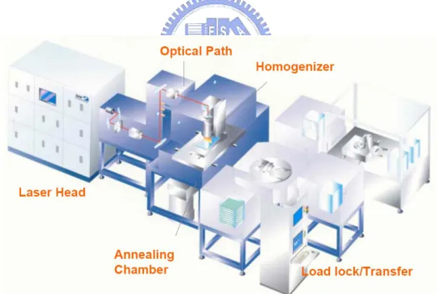
(42) vacuum ultraviolet (Ultraviolet radiation that has a wavelength of less than about 200 nm), a further output arising from the molecule fluorine (F2) transition at 157 nm is available, although the output on the gas mix is weaken than any of those just listed. Typical outputs on the stronger transitions are pulse energies of a few hundred to one thousand mJ, and repetition rates of 10 Hz to a few hundreds Hz. In some case, repeation rates of up to 1 kHz are available. Typical excimer lasers operate in pulse mode, at frequencies around 300 Hz. Average powers are normally in the 10- to 300-W range. The pulse width of the excimer lasers is short, typically in 10-50 ns range. This results in peak powers of several tens of megawatts [30].. Fig. 2-5: Schematic of a typical excimer laser annealing (ELA) system. It is used for LTPS of large size LCD substrate manufacture. This ELA system includes Laser head, optical path, homogenizer, annealing chamber, and transfer controller [31]. 25.
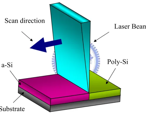
(43) Fig. 2-5 is a Schematic of a typical excimer laser annealing (ELA) system. Excimer laser annealing (ELA) systems use Long beam homogenizer. to make excimer laser beam’s energy cindidtent he. amorphous silicon film for uniform annealing results. Excimer lasers have typically a rectangular beam profile, whereas the long axis has a top head and the short axis has a Gaussian like shape [32].. Scan direction. Laser Beam. Poly-Si. a-Si. Substrate. Fig. 2-6: Principle of excimer laser annealing. The pulsed excimer laser beam is homogenized and shaped to a line and scanned across the surface. Within the laser pulse duration the amorphous silicon layer is rapidly heated and melted. As it cools down the recrystallization into polycrystalline silicon occurs.. 26.
(44) In LPTS- TFT laser annealing process the laser beam is formed to a line shape. This modified beam with an adjustable width between 0.1 and 1.0 mm and a length of up to 370 mm is scanned over the amorphous silicon (see Fig. 2-6). For increasing display size lasers with higher output power are required in order to achieve sufficient laser energy density on the target. The recent high power excimer lasers for silicon annealing deliver 300 W (i.e. 1 Joule at 300 Hz) [32]. Analysis of the transformation methods associated with ELA, show that one can categorize ELC of Si films in terms of three transformation regimes (occurring at partial melting, nearly complete melting and complete melting, respectively) [33]. The partial melting regime describes the situation that is encountered when the incident energy density of the laser pulse is sufficient to induce melting of amorphous or crystalline silicon films, but is low enough such that a continuous layer of solid silicon remains at the maximum extent of primary melting. For irradiation of amorphous silicon films, this regime is characterized by a combination of explosive crystallization and vertical solidification; explosive crystallization can be triggered at the onset, or near the end of melting, depending on the presence or absence of microcrystals, respectively [34]. The complete melting regime describes the situation that is encountered when the incident energy density is sufficiently high such that it leads to complete melting of the film. The nucleation in the case takes place as a result of the unusually deep undercooling that occurs in the molten-Si film. In the sense, deep undercooling implies a liquid existing at a temperature substantially lower than its melting point. As a 27.
(45) result of the copious nucleation that occurs within the undercooled molten-Si, the grain sizes obtained in the regime are very small. The third regime has been found to exist within a very narrow experimental window. This regime describes the situation that is encountered when the incident energy is almost sufficiently high such that it leads to nearly compltet melting of the film; it is also referred to as the nearly complete melting regime. This is a noteworthy regime in that either single or multiple irradiations of a-Si or polycrystal- line Si films within the regime can lead to the formation of large-grained polycrystal microstructures. [36] Practically, it was argued that at the maximum extent of melting, the unmelted portion of the underlying Si film no longer form a continuous layer, but instead consists of discrete islands of solid state material. separated. by. small. regions. that. have. undergone. complete-melting. The unmelted islands provide solidification “seeds”, from which lateral growth can ensue, thus propagating the solid-liquid interface within the surrounding undercooled molten silicon [11,34,35]. The three kinds recrystallization regime of excimer laser annealing (ELA) is shown in Fig. 2-7 respectively.. 28.
(46) During irradiation (a) Partial melting. Crystallized film. -. molten solid. (b) Nearly complete melting. molten. Fine grain / amorphous. Large grain. Nucleation on solid regions Super Lateral Growth (SLG). solid. (c) Complete melting. Medium grain. molten. Fine grain. Random nucleation in super cooled melting layer. Fig. 2-7: Three regimes of ELA includes partial melting, nearly complete melting and complete melting. The nearly complete melting between the other two regimes is also called super lateral growth (SLG) of excimer laser annealing (ELA).. The nature of the SLG phenomenon dictates that when one controls the locations of the silicon film that undergoes localized complete melting (which may be accomplished via a number of technical schemes), then the resulting solidification will proceed so as to produce entirely predictable and large-grained microstructures. Specifically, it implies that inducing complete melting of the film only at small and well-defined regions will inevitably lead to the formation of microstructures that consist of large grains that are elongated in the direction of the lateral 29.
(47) solidification. Such microstructures are formed as a consequence of the lateral solidification that commences from the solid-liquid interface at the boundary between the completely and incompletely molten regions and grows into the completely molten areas [36].. 2 - 5 µm. ~ 500 µm Laser Beam Si. molten. Si. Substrate. Si. Poly-Si. Substrate. Grain boundary. Substrate. Substrate. Fig. 2-8: Comparison of SLG and C-SLG modes of growth. In SLG (left panels) growth initiates from seeds, which survived the melting process, at the Si-SiO2 interface. In C-SLG (right panels) the poly-Si microstructure forms by lateral epitaxy from seeds generated at the liquid-solid interface. Notice the difference in the width of the molten zone between SLG and C-SLG.. 30.
(48) The maximum length of the C-SLG grown grains that can be attained using a singlepulse irradiation will be limited by nucleation to a few micrometers. There will always be an associated degree of limitations in controlling the resulting microstructure. For those C-SLG approaches that utilize shaping of the incident beam, however, a potent option exists for trivially overcoming the above limitation inherent with singlepulse irradiation. By simply and appropriately repositioning the relative position of the sample with respect to the incident beam between pulses, it is possible to induce further lateral growth of the previously formed grains via epitaxial growth by seeding from the grains (see Fig. 2-8). This special process of iteratively inducing C-SLG in a coordinated manner is referred to as sequential lateral solidification (SLS), and it represents an effective and efficient means to manipulate the microstructure of a thin Si film [37,38]. The nature of the SLS process dictates that, in addition to the basic C-SLG requirement of inducing complete melting in controlled locations, the following conditions are to be satisfied: 1. the relative translation be in the direction of the lateral growth and 2. the per-pulse translation distance be less than the C-SLG distance. Satisfying these additional conditions ensures that the subsequent irradiation leads to continuous epitaxial lateral growth of the grains [36].. 31.
(49) 2.2.3 Femtosecond Laser Annealing (FLA) Femtosecond laser pulses impart extremely high intensities and provide precise laser-ablation thresholds at substantially reduced laser energy densities. Femtosecond laser induced phase transitions in covalently bonded semiconductors have been extensively studied during the past decade. On excitation with a femtosecond pulse, a semiconductor undergoes several stages of relaxation before returning to equilibrium. The energy is transferred first to the electrons and then to the lattice. The interaction includes several regimes of carrier excitation and relaxation. We can distinguish the following four regimes: (1) carrier excitation, (2) thermalization, (3) carrier removal and (4) thermal and structural effects [39]. These regimes and the timescales for the corresponding processes are shown in Fig. 2-10.The triangles at the top of the figure mark the current state-of-the-art in the generation of ultrashort pulses of various wavelengths. In the visible region, pulses as short as 5 fs allow direct probing of carrier dynamics down to the shortest timescales (triangle 1). Diffraction of hard X-ray pulses of 200 fs duration (triangle 2) permit observation of structural and atomic rearrangements in the bulk of materials, but not the carrier excitation and carrier–lattice interaction processes that precede the structural dynamics, because X-rays cannot see electrons. The shortest pulses obtained to date, of 800-as duration (triangle 3), are in the soft X-ray region, and are limited to probing corelevel transitions in excited atoms [15].. 32.
(50) Fig. 2-9: Timescales of various electron and lattice processes in laser-excited solids. Each green bar represents an approximate range of characteristic times over a range of carrier densities from 1017 to 1022 cm–3. The triangles at the top show the current state-of-the-art in the generation of short pulses of electromagnetic radiation: 1 5 fs (visible), 2 120 fs (X-ray), 3 0.5 fs (far ultraviolet) [15,39].. For picosecond and subpicosecond laser pulses, however, ample experimental evidence exists from Shank and co-workers [40] and other groups, that nonthermal structural changes can be driven directly by electronic excitation [41]. According to the so-called non-thermal plasma model, the lattice is disordered by direct excitation of the electronic system, while the lattice modes remain vibrationally cold. Absorption of photons creates a free carrier plasma and, when about 10% of valence 33.
(51) electrons are removed from bonding orbitals, the lattice is weakened. Photoexcitation can thus give the atoms enhanced mobility without increasing their thermal energy. The non-thermal model assumes that the rate of phonon emission by the excited electronic system is slow compared with the laser pulse duration. When this assumption is satisfied, and a large enough fraction of the valence electrons is excited, structural change can occur while the electronic system and the lattice are not in thermal equilibrium with each other, although each of these systems may internally be in quasi-equilibrium [39]. Mechanisms of femtosecond laser-induced ablation on crystalline silicon are investigated by time-resolved pump-and-probe microscopy in normal imaging and shadowgraph arrangements. The imaging with the time-delayed frequency-doubled probe beam had a temporal resolution of 100 fs. The high electron temperatures and dense solid-state plasma formation suggest a non-equilibrium phase transition process. Thermionic emission and photoemission of electrons can initiate air plasma in the proximity of the surface. Time-resolved shadowgraphs of the shock wave propagation show that the ultrafast initial plasma becomes visible at around 10 ps and is followed by a slower ‘‘thermal’’ contribution in the time scale of 30 ns. The instantaneous energy released upon initiation of explosion is estimated to be 10%–17% of the absorbed laser energy depending on the incident laser energy. The pressure of the released shock wave was calculated to be about a few hundreds of atm [18]. Our group had presented a near-infrared femtosecond laser annealing with 50 fs pulse duration. The intense femtosecond laser pulses lead to efficient nonlinear photon adsorption in irradiated materials, 34.
(52) enabling a melting of amorphous silicon films. Femtosecond laser annealing (FLA) assisted by a scanning of the laser beam efficiently crystallizes amorphous silicon films with large average grains of 800 nm, using a total laser energy as low as ~ 0.9 J /cm2 [21]. The results of near-infrared femtosecond laser annealing are described in section §4.1. Then the comparisons between near-infrared femtosecond laser annealing and blue femtosecond laser annealing is also given. Up to now, a clear distinction of the transition between the ultrafast liquid phase and the electron-hole plasma state is hard. However, it is undoubted that the classical thermal model of crystallization mediated cannot explain the subpicosecond rapid phase transition satisfactorily.. 35.
(53) Chapter 3 Experimental Methods In chapter 3, our sample preparation is mentioned. After that, a brief introduction to our femtosecond laser pulse and the frequency doubling process separately are described. Then we could see the experimental components completely in the schematic diagram of experiment setup in section §3.3. In section §3.4, the characterizations of blue femtosecond laser annealing samples which include scanning electron microscope (SEM) images and Raman spectra are presented finally.. 3.1 Sample Preparation The amorphous silicon samples were prepared by National Nano Device Laboratory (NDL). The scheme of the LPCVD device is shown in Fig. 3-1. The base of device is a quartz tube placed in a spiral heater. The tube is evacuated on the pressure of 0.1 Pa and heated on to the wanted temperature to 1000 °C. The temperature stability is +/- 1 °C. The deposition starts with entering of the working gas in the tube. The working (dynamical) pressure is 10-1000 Pa. The working gas, that regularly consist of the gas for dilution and of the reactive gas, after entering spreads inside the tube and flows above the hot substrates (thin pates of silicon, quartz or some other material) placed in the quartz holders. The critical factors that influence on thickness uniformity and film content are positions of the substrates, temperature profile in the 36.
(54) zone of deposition, reactor geometry, deposition time, working pressure, as well as the quantity and content of all gases or vapor that enter in the reactor.. Furnace with heaters. Substrate plates Exhaust system Trap. Vacuum pump gas flow control. Gas source H2. SiH4. Fig. 3-1: Schematic description of LPCVD device.. The typical reaction is: SiH4 → Si + 2H2. Then, Silane-based amorphous silicon films were deposited on oxidized (500 nm) silicon wafers by low-pressure chemical vapor deposition (LPCVD) at 550 °C. The thickness of amorphous silicon is 100nm and the wafer’s original thickness is 500 nm (SiO2). 37.
(55) 3.2 The Blue Femtosecond Laser System 3.2.1 Introduction to Femtosecond Laser System The invention of the laser in 1960 stimulated renewed interest in optical physics and gave rise to a number of new research fields. One of them was the field of ultrafast optics, which had the beginning in the mid-1960s with the production of nanosecond (10-9 s) pulses by the first mode-locked laser. Today, femtosecond pulse generation remains the subject of active research. Rapid progress in this field has led to the creation of practical and useful lasers that can now produce pulses on the femtosecond (10-15 s) time scale. This section gives a brief introduction to our femtosecond laser pulse. Our femtosecond laser system is shown in Fig. 3-2. We use the Ti:Sapphire laser as the seeding laser which is then directed into the Ti:Sapphire regenerative amplifier (Spitfire, Spectra-Physics) for amplification. Fig. 3-3 shows the schematic view of the Spectra Physics Tsunami laser head. The pump beam is a 5W frequency doubled diode-pumped Nd:YVO4 laser (Millennia V, Spectra-Physics) with a wavelength λ = 532 nm as shown in Fig. 3-3. The titanium sapphire laser provides an output trace of intense 35 fs pulses with wavelengths ranging from 750 nm to 850 nm (standard optics set). The property of the Ti:Sapphire laser is shown in Table 3-1. The pulse repetition rate is ~82 MHz and the output power is up to 0.5 W.. 38.
(56) 800 nm, 50 fs, 0.8mJ. Evolution X. Ti:Sapphire Regenerative amplifier (Spitfire, Spectra-Physics). Nd:YLF laser for pumping amplifier. Nd:YVO4 laser for pumping Millennia V. Ti:Sapphire laser for seed beam (Tsunami, Spectra-Physics). Fig. 3-2: Femtosecond laser system includes Tsunami, Spitfire, and two pump laser (Millennia V and Evolution X).. Fig. 3-3: Tsunami femtosecond cavity layout [42].. 39.
(57) pulse width. 35 fs. band width. 45 nm. power. 500 mW (@ 5.0 W pump power). beam diameter. 2 mm. beam divergence. 0.6 mrad. polarization. vertical, linear. Table 3-1: Spectra Physics Tsunami specifications. The driver for the amplification process in the Spitfire is a frequency doubled Diode-pumped Nd:YLF laser. The Spitfire amplifies the original seeding pulses by a million times from 5 nJ of energy per pulse to 800 µJ per pulse. The chirped-pulse amplification diagram is shown in Fig. 3-4. The pulse repetition rate is 1 kHz and the pump power is 11-13 W for the Nd:YLF laser. The property of the Spitfere is shown in Table 3-2.. Stretching. Amplificatio. Compression. Fig. 3-4: The Spitfire amplification process.. 40.
(58) Wavelength. 800 nm. Repetition rate. 1 kHz. Pulse duration (FWHM). 50 fs. Energy. 800 µJ. Beam diameter. 15 mm. Energy stability. <2%. Polarization. linear, horizontal. Table 3-2: The specifications of the regenerative amplifier. 41.
(59) 3.2.2 Characterization of Blue Femtosecond Laser Pulse Finally, a type I BBO nonlinear crystal was used as second harmonic generator. BBO crystal or β-BaB2O4 is a nonlinear optical crystal which combines a number of unique features. These features include wide transparency and phase matching ranges, large nonlinear coefficient, high damage threshold and excellent optical homogeneity. Chemical and structural properties of the BBO crystal are shown in Table 3-3. Optical and nonlinear optical properties of BBO crystal are shown in Table 3-4. Therefore, it provides an attractive solution for various nonlinear optical applications. Application in femtosecond pulse laser frequency doubling and frequency tripling of femtosecond pulse lasers are the applications in which BBO shows superior properties to KDP and ADP crystals. The setup of the blue femtosecond generation is shown in Fig. 3-5. We could see the red and blue beam paths in it. We use two dichroic mirror (HR @ 400 nm and HT @ 800 nm) to filter out the fundamental beam. Then, the blue femtosecond laser’s pulse width is 50fs with repetition is 1kHz and the pulse of energy ranging from 50 mJ to 90mJ. We measure the power transformation of the frequency doubling setup. The results of the power transformation from 400 nm to 800 nm are plotted in double-logarithm scale as shown in Fig 3-6. We could see the blue light which is reflected to the opposite direction in Fig. 3-5 obviously. We have considered the reflective light from the backside of BBO crystal. The slope of the power transformation ratio is 1.6 42.
(60) approximately and the power transformation efficiency is about 17%. The slope of the frequency doubling is not 2 (theoretical value).. Fig. 3-5: The frequency doubling setup in the experiments.. Output power at 400nm. 100. Linear Fit. 10. 1 10. 100. 1000. Input power at 800nm. Fig. 3-6: The frequency doubling power transformation ratio.. 43.
(61) Crystal Structure. Trigonal, space group R3c. Lattics Parameters Melting point. a=b=12.532Å, c=12.717Å, Z=6 About 1095℃. Mohs Hardness. 4. Density. 3.85g/cm3. Thermal Conductivity. 1.2W/m/K(┴c) ; 1.6w/m/K(//c). Thermal Expansion Coefficients. α,4x10-6/K ; c,36x10-6/K. Table 3-3: Chemical and structural properties of BBO crystal [43].. Transparency Range. 190-3500nm 409.6-3500nm(TypeI) 525-3500nm(Type II) dno/dT=-9.3x 10-6/℃ dne/dT=-16.6x 10-6/℃. SHG Phase Matchable Range therm-optic Coefficients(/℃). <0.1%/cm at 1064nm <1%/cm at 532nm. Absorption Coefficients. 0.8mrad-cm (θ, Type I,1064 SHG) Angle Acceptance Temperature Acceptance. 1.27mrad-cm (θ, Type II,1064 SHG) 55℃-cm. Spectral Acceptance. 1.1nm-cm 2.7°(Type I 1064 SHG). Walk-off Angle 3.2°(Type II 1064 SHG) deff (I)=d31sinθ+(d11cosΦ-d22sin3Φ)cosθ NLO Coefficients deff (II)=(d11sin3Φ+d22cos3Φ)cos2θ Non-vanished NLO susceptibilities. d11=5.8xd36(KDP) ; d31=0.05xd11 ; d22<0.05xd11. sellmeier Equations (λ in µm ). no2=2.7359+0.01878 / (λ2-0.01822) -0.01354λ2 ne2=2.3753+0.01224 / (λ2-0.01667) -0.01516 λ2. Electro-optic coefficients. r11=2.7pm/V ; r22 ; r 31<0.1γ11. Half-wave voltage. 48Kv (at 1064nm). Resistivity. >1011 ohm-cm. Relative Dielectric Constant. εs11/εo:6.7 ; εs33/εo:8.1 ; Tan δ<0.001. Table 3-4: Optical and nonlinear optical properties of BBO crystal [43].. 44.
(62) 3.3 The Laser Annealing station A schematic of the experimental apparatus is shown in Fig. 3-7. A femtosecond mode-locked seeding beam of 50 fs pulse duration and 800nm of central wavelength, carrying pulse energies in the sub-mJ range at a repetition rate of 1 kHz, is emitted from a Ti:sapphire regenerative amplifier. A type I BBO nonlinear crystal was used as second harmonic generator. Blue femtosecond pulse of energy ranging from 50 µJ to 90 µJ was obtained after nonlinear crystal. Then, he blue femtosecond laser with a wavelength of 400 nm was guided to crystallize amorphous silicom. Two dichroic mirrors with HR @ 400 nm and HT @ 800 nm were used to filter out the residual 800 nm fundamental beam. Silane-based a-Si films (100 nm) were deposited on oxidized (500 nm) silicon wafers by low-pressure chemical vapor deposition (LPCVD) at 550 °C. All amorphous silicon samples were placed in a vacuum chamber, and the substrate temperature is the room temperature. The femtosecond pulse train from the forementioned laser system was focused in the strip spot (105µm × 2850µm). Fig. 3-8 (a) is the photo of the annealing chamber. The chamber could increase the substrate temperature up to 400 °C. Fig. 3-8 (b) is the X-Y transition stage in our experiment setup. In the blue femtosecond laser annealing experiment, the overlapping of the laser beam changes from 85% to 97.5% (i.e. 2.5-15 mm/s, or equivalently 5-40 laser shots per unit area). On the other hand, the fluence ranges from 20 mJ/cm2 to 30 mJ/cm2.. 45.
(63) M1. M1. M1. 1KHz Reg. Amp. (~800nm, 50fs). BBO/SHG. DM. Beam expander. DM. Block. 4mm M1. Transition stage X. 15mm M1. M2. Y. M1: IR dielectric mirror M2: Blue dielectric mirror DM: dichroic mirror. control Vacuum chamber. (HR@400nm/HT@800nm). Fig. 3-7: Schematic diagram of blue femtosecond laser annealing experiment setup. (a). (b). Fig. 3-8: Our femtosecond laser annealing chamber and transition stage. (a) Blue femtosecond laser annealing setup – vacuum chamber. (b) Blue femtosecond laser annealing setup –XY transition stage. 46.
(64) 3.4 Characterization of Annealing Samples Scanning electron microscope (SEM) pictures of annealed areas with obvious grain boundaries, obtained by delineating defects using Secco etching. A series of the blue femtosecond laser annealing scanning electron microscope (SEM) images are shown below which illustrate the variation in grain size distribution for different overlapping (i.e. number of pulses) and fluence. From Fig. 3-9 to Fig.3-16, the eight figures represent line-scan FLA samples irradiated with changed interpulse overlapping of 50 fs with different energy densities at room temperature. In Fig.3-9, we plot the relationship between average grain seize and changed overlapping as the flunce is 20 mJ/cm2. We could see the average grain seize curve is flat before the overlapping up to 92.50%. The average grain size is relatively small (lower than 60 nm) and almost independent on the energy density (see Fig. 3-9). In Fig.3-10, we plot the relationship between average grain seize and changed overlapping as the flunce is 21.7 mJ/cm2. We could observe a relationship the same with Fig. 3-9. The average grain seize curve is flat before the overlapping up to 92.50%. After the overlapping increased to 92.50%, the grains have a growth and the average grain size is larger than the lower fluence at the same overlapping condition. Then the Fig. 3-11, Fig. 3-12, and Fig, 3-13 almost have the same trend which means the grain grow larger as overlapping up to 90.00%. When we increase the overlapping at the same fluence, there will be more enegy absorbed by amorphous silicon layer to excite the electrons from valence. 47.
(65) band to conduction band. Then the annealed amorphous silicon translates into polycrystalline silicon. Fig. 3-14 and Fig.3-15 give the more significant grain growth phenomenon. There seems to be a threshold of overlapping as the fluence is 28.3mJ/cm2 in Fig. 3-14. Fig.3-15 has a trend is like to Fig. 3-14, but the threshold in Fig. 3-15 is obviously. After increasing the overlapping larger the threshold, the grain size decrease oppositely. We could expect the transformation threshold would be changed in different fluence conditions. It seems to be reasonable that the higher fluence indicates the lower overlapping threshold as our experimental results. The overlapping threshold at 30.0 mJ/cm2 (93.75%) is lower than the overlapping threshold at 28.3 mJ/cm2 (96.25%). Finally for making a summary, we combine the seven Figures from Fig. 3-19 to Fig. 3-15 into Fig. 3-16. Another interesting property in the seven figures is the growth trend which has a similar recrystallization property to sequential lateral solidification (SLS) in excimer laser annealing (ELA) mentioned in section §2.2.3. The sequential lateral solidification (SLS) describes the recrystallization methods in excimer laser annealing (ELA) by departing the three kinds of melting amorphous silicon (a-Si). They are partial melting, nearly complete melting and complete melting. We could get the largest grain at the nearly complete melting. In this condition the grain shape is longitudinal. We could find the longitudinal grain shape in Fig. 3-12, Fig. 3-13, Fig. 3-14 and Fig. 3-15. In Fig. 3-12 the scanning electron microscope (SEM) images show the longitudinal shape of grain apparently. Fig. 3-12’s SEM images looks. 48.
(66) like the SEM images which use sequential lateral solidification (SLS) in excimer laser annealing (ELA) as mentioned in section §2.2.3.. Fig. 3-9: Average grain seize versus overlapping at 20.0 mJ/cm2.. 49.
(67) Fig. 3-10: Average grain seize versus overlapping at 21.7 mJ/cm2.. Fig. 3-11: Average grain seize versus overlapping at 23.3 mJ/cm2. 50.
(68) Fig. 3-12: Average grain seize versus overlapping at 25.0 mJ/cm2.. Fig. 3-13: Average grain seize versus overlapping at 26.7 mJ/cm2. 51.
(69) Fig. 3-14: Average grain seize versus overlapping at 28.3 mJ/cm2.. Fig. 3-15: Average grain seize versus overlapping at 30.0 mJ/cm2. 52.
(70) Fig. 3-16: Average grain seize versus overlapping as the flunce changes.. 53.
(71) Then we will discuss the relationship between grain size and fluence at room temperature in the paragraph. Fig.3-17, Fig.3-18, Fig.3-19, Fig.3-20, Fig.3-21, Fig.3-22, Fig.3-23, and Fig. 3-24 all show the relationships between changed fluence (20 mJ/cm2 - 30 mJ/cm2) and average grain size at different overlapping conditions after line-scan by blue femtosecond laser annealing. From Fig. 3-17 to Fig. 3-21, we could easily see the relationship as increasing the fluence at the fixed overlapping condition, the average grain size will also grow up. In Fig. 3-17, we could see the grain starting growing until fluence is 30.0 mJ/cm2 under 85.00% overlapping. It seems to be a flat average grain size curve (lower than 60 nm) which is almost independent on the changed fluence. As the overlapping is 87.50%, the starting point of grain size growing is at 28.3mJ/cm2 which is earlier than 85.00% overlapping (see Fig. 3-18 and Fig. 3-17). The same result is shown in Fig. 3-19 and Fig. 3-18. Because of the lower overlapping, we need to serve the higher fluence to make phase transition. It means the same area absorbed lower energy at lower overlapping than higher overlapping. But it does not mean that the high fluence is better than lower fluence at the same overlapping. We still need to consider the ablation threshold to prevent from destroying the amorphous silicon layer. We will discuss the concept in chapter 4. Now we keep on discussing the results. It seems to need to absorb enough energy to get the amorphous silicon to be recrystallized (see Fig. 3-20 and Fig.3-21). The grains grow large as the fluence is increased at the same overlapping. We could also see that the higher fluence will produce the larger average grain size. In Fig. 3-22, we could see the 54.
(72) growing grain size trend and the threshold of the average grain size. It is apparent in Fig. 3-24 especially. We observe that the fluence increased over the threshold will not produce the larger grain size. After increasing the fluence larger the threshold, the grain size decrease oppositely. We could expect the transformation threshold would be changed in different overlapping conditions. It seems to be reasonable that the higher fluence indicates the lower overlapping threshold as our experimental results. We have discussed the phenomenon just now. Then we combine the eight figures (from Fig. 3-17 to Fig.3-24) into Fig. 3-25. We could see that there seems to be a grain size limitation in the room temperature condition. The limited grain size is about 280nm in the blue femtosecond laser annealing at room temperature. And the apparent difference between 90.00% overlapping (see Fig. 3-19) and 92.50% overlapping (see Fig. 3-20) we also discussed in previous pages.. 55.
(73) Fig. 3-17: Average grain seize versus fluence as 85.00% overlapping.. Fig. 3-18: Aaverage grain seize versus fluence as 87.50% overlapping. 56.
(74) Fig. 3-19: Average grain seize versus fluence as 90.00% overlapping.. Fig. 3-20: Average grain seize versus fluence as 92.50% overlapping. 57.
(75) Fig. 3-21: Average grain seize versus fluence as 95.00% overlapping.. Fig. 3-22: Average grain seize versus fluence as 95.00% overlapping. 58.
(76) Fig. 3-23: Average grain seize versus fluence as 96.25% overlapping.. Fig. 3-24: Average grain seize versus fluence as 97.50% overlapping. 59.
(77) Fig. 3-25: Average grain seize versus flunce as the overlapping changes.. 60.
(78) In Fig. 3-26, the sample was characterized by Raman scattering using the 514 nm line of an Ar+ laser. Raman scattering reveals if a film is amorphous, crystalline, or mixed phase. Amorphous-Si has a broad peak at ~ 480 cm-1, and crystalline Si has a sharp peak at ~ 520 cm-1. Both the peak widths and positions can change slightly due to stress and crystallite size.. 1.1 1.0. Raman Intensity (a.u). 0.9 0.8 0.7 0.6 0.5 0.4 0.3 0.2 0.1 0.0 440. 460. 480. 500. 520. 540. 560. 580. 600. 620. -1. Raman Shift (cm ). Fig. 3-26: This sample was produced as fluence is 30 mJ/cm2 and overlapping is 93.75% at room temperature. The sharp peak centered at ~ 519.5 cm-1. The FWHM is ~ 7.5 cm-1.. 61.
(79) (a). (b). Image Statistics Img. Rms: 9.067 nm. Image Statistics Img. Rms: 12.614 nm. (c). Image Statistics Img. Rms: 62.646 nm. Fig. 3-28: (a), (b), and (c) are AFM images of blue FLA poly-Si films irradiated with 50 fs pulses. (a) fluence of 28.3mJ/cm2 and an interpulse overlapping of 90.0%. (b) fluence of 28.3mJ/cm2 and an interpulse overlapping of 92.5%. (c) fluence of 28.3mJ/cm2 and an interpulse overlapping of 96.25%.. The rms roughness measured by atomic force microscopy (AFM) of is 9.067 nm as fluence of 28.3mJ/cm2 and an interpulse overlapping of 90.0% as shown in Fig. 3-28(a). The rms roughness is 12.614 nm as fluence of 28.3mJ/cm2 and an interpulse overlapping of 92.5% as shown in Fig. 3-28(b). The rms roughness is 62.646 nm as fluence of 28.3mJ/cm2 and an interpulse overlapping of 96.25% as shown in Fig. 3-28(c). The rms roughness is much larger than the value in Fig. 3-28 (a) and (b). Because of the overlapping condition in Fig. 3-28(c) is over the threshold. Then the poly-Si layer is damaged by the bule femtosecond laser.. 62.
數據
+7
![Fig. 2-3: The difference of aperture ratio between a-Si TFT and poly-Si TFT [23].](https://thumb-ap.123doks.com/thumbv2/9libinfo/8719793.200445/36.892.106.782.213.487/fig-difference-aperture-ratio-si-tft-poly-tft.webp)
相關文件
The closing inventory value calculated under the Absorption Costing method is higher than Marginal Costing, as fixed production costs are treated as product and costs will be carried
* All rights reserved, Tei-Wei Kuo, National Taiwan University, 2005..
Figure 6.19 The structure of a class describing a laser weapon in a.
In flow field boarding up for the smooth wall surface, gets down the board is the Sinusoidal wavy wall, but under board wavy wall oscillation amplitude A=2.54(mm), the wave length λ
This research project is to analyze and research a specific laser configuration to obtain complete knowledge、technologies and experiences to transfer to the project initiator for
We have investigated, designed, and completed the testing of the novel auto leveling, multiple-directing, high refined laser light line red and green laser cross line indictor..
Courtesy: Ned Wright’s Cosmology Page Burles, Nolette & Turner, 1999?. Total Mass Density
For ASTROD-GW arm length of 260 Gm (1.73 AU) the weak-light phase locking requirement is for 100 fW laser light to lock with an onboard laser oscillator. • Weak-light phase
