Sub-I
V CMOS large capacitive-load driver
circuit using direct bootstrap technique for
'
low-voltage CMOS VLSI
P.C. Chen
andJ.B. Kuo
A novel sub-l V CMOS large capacitive-load driver circuit using a
direct bootstrap technique for low-voltage CMOS VLSI is reported. For a supply voltage of 1 V, the CMOS large capacitive-load driver circuit using the direct bootstrap technique shows a 3.3 times improve- ment in switching speed in driving a capacitive load of 2 pF compared to the conventional bootstrapped CMOS driver circuit using an indirect bootstrap technique. Even for a supply voltage of 0.8 V, this
CMOS large capacitive load driver circuit using the direct bootstrap technique is still advantageous.
Introduction: Nowadays the design of the driver circuit is the key step in determining the speed performance of a CMOS VLSI circuit with a large capacitive load. Indirect bootstrap techniques to raise/lower the gate voltage of the output NMOS/PMOs device have been used in the large load driver circuit using a low power supply voltage [l-31. Since the bootstrap technique is applied at the gate of the output devices in a driver circuit, it is categorised as the indirect bootstrap technique. The indirect bootstrap technique via the gate of the output device may not be effective in shortening the switching speed of the output. Recently, low power supply voltage is the trend on the future CMOS VLSI circuits. Since the magnitude of the threshold voltage of the CMOS devices cannot be scaled down accordingly with the power supply voltage, the design of an effective large load driver circuit using down-scaled CMOS devices with a low power supply voltage is challenging. In this letter we describe an effective large load CMOS driver circuit using a novel direct bootstrap technique applied on the output. The direct bootstrap technique used in a large load CMOS driver circuit is described first, followed by the performance evalua- tion and discussion.
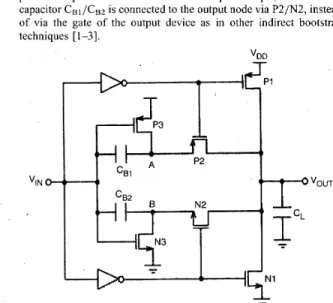
Direct bootstrap technique: Fig. 1 shows the sub-I V large load driver circuit with the direct bootstrap technique. As shown in the Figure, this circuit is composed of three NMOS devices N1-N3, three PMOS devices PI-P3, and two inverters. In addition, two bootstrap capacitors CBl and CB2 have been used to implement the direct bootstrap technique. Among these devices, PMOS devices P 1 -P3 and the bootstrap capacitor CBI are used for the pullup operation; NMOS devices Nl-N3 and the bootstrap capacitor C B ~ for the pulldown operation. In this direct bootstrap technique, the bootstrap capacitor CBl/CBz is connected to the output node via P2/N2, instead of via the gate of the output device as in other indirect bootstrap techniques [l-31.
"IN
Fig. 1 Sub-I V CMOS large capactive load driver circuit using direct bootstrap technique
Performance and discussion: To assess the performance of the large load driver circuit using the direct bootstrap technique, a test circuit
based on a 0.18 pm CMOS technology has been designed. The channel length of all devices in the circuit is 0.18 pm. The channel width of the NMOS/PMOS devices is 40 pm/80 pm. Fig. 2 shows the transient waveforms of the sub-1V large load CMOS driver circuit using the direct bootstrap technique with an output load of 1 pF and the bootstrap capacitors of 0.35 pF at a power supply voltage of 1V based on SPICE simulation results. As shown in Fig. 3a, prior to the pullup operation, the input voltage Vi, = 0 V P3 is on and N2 is on. Under this situation, the bootstrap capacitor CB1 is charged to 1V since its right side is connected to 1 V via P3 and the left side is at 0 V At the same time, the bootstrap capacitor CB2 is charged to 0 V since both sides are connected to 0 V. As shown in Fig. 36, after the input ramps up to 1 V, N3 is on and P2 is on. Therefore, the right side of the bootstrap capacitor CBI is connected to the output node. Owing to the charge stored in the bootstrap capacitor CBI , from the positive jump at the input from 0 to 1 V, the internal node A is bootstrapped to 1.35 V As a result, the output V,,, is quickly raised to 1 V As shown in the Figure, the output V,,, may surpass 1 to 1.1 V for a short period time. During the pulldown operation, the scheme is complementary. Prior to the pulldown operation, the bootstrap capacitor C B ~ is charged to -1 V via N3. After the input ramp-down period, owing to the stored charge in the bootstrap capacitor CB2, the internal node B is bootstrapped to below 0 V As a result, the pulldown time of the output has been shortened.
-0.4
';
0 0.5 1 .o 1.5 2.0 2.5
time, ns
Fig. 2 -Transient waveforms during pullup operation of sub-I V CMOS large cupactive load driver circuit with direct bootstrap technique Bootstrap capacitors 0.35 pF, output load 2 pF, at power supply voltage of 1 V
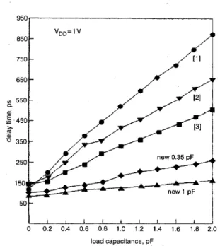
Fig. 4 shows the pullup propagation delay time against load capaci- tance of the large load CMOS driver circuit using the direct bootstrap technique with bootstrap capacitors of 1 and 0.35 pF. Also shown in the Figure are the results of the driver circuits using the indirect bootstrap techniques [ 1-31, For a load capacitance of 2 pf, the speed improvement of the driver circuit using the direct bootstrap technique over the indirect bootstrap one [ l ] is 3.3 times. Different from the other indirect bootstrap one, the direct bootstrap technique used in this driver circuit is more effective in enhancing the switching speed. The effectiveness of the direct bootstrap technique used in the driver circuit is determined by the bootstrap capacitors (CBl, CB2). As shown in Fig. 4, with large bootstrap capacitors of 1 pF, the switching time is shortened further, which is especially noticeable with a large output capacitive load. The size of the bootstrap capacitor is limited by the amount of the voltage overshoot/undershoot beyond 1 V/0 Vat the internal node A/B during pullup/pulldown, which may cause the forward bias of the pn junction between source/drain-substrate. As shown in Fig. 2, with bootstrap capacitors of 0.35 pF, the voltage overshoot/undershoot at the internal node A/B is about 0.35 V/ - 0.35 V, which causes a minor leakage current of the pn junction between source/drain-substrate of the P2 and P3/N2 and N3 devices.
Conclusion: A novel direct bootstrap technique used in a sub-I V CMOS large capacitive-load driver circuit for low-voltage CMOS VLSI has been described. For a supply voltage of 1 V, the CMOS large capacitive load driver circuit using the direct bootstrap technique
shows a 3.3 times improvement in switching speed in driving a capacitive load of 2 pF compared to the conventional bootstrapped CMOS driver using an indirect bootstrap technique. This sub-1 V
CMOS large load driver circuit using the direct bootstrap technique can still be advantageous at a power supply voltage of 0.8 V.
1v T
I
T a 1v T b*
Fig. 3 Equivalent circuit of CMOS large capacitive load driver circuit with direct bootstrap technique during pullup operation
50
t
0 0.2 0.4 0.6 0.8 1.0 1.2 1.4 1.6 1.8 2.0 load capacitance, pF
Fig. 4 Pullup delay time against load capacitance of sub-I V CMOS large capacitive-load driver circuit with direct bootstrap technique
Acknowledgments: This work is supported under research grants from NSERC in Canada and NSC in Taiwan.
0
IEE 2002Electronics Letters Online No: 20020208 DOI: 10.1049/e1:20020208
17 December 2001
J.B. Kuo (Department of Electrical & Computer Engineering, DC2737, University of Waterloo, Waterloo, Ontario, Canada N2L 3 G l )
E-mail: jbkuo@uwaterloo.ca
P.C. Chen (Department of Electrical Engineering, National Taiwan University, Roosevelt Rd., Sec. 4, No. I , Taipei, Taiwan 106-1 7) References
1 LOU, J.H., and KUO, J.B.: ‘A 1.5-V fullswing bootstrapped CMOS large capacitive-load driver ‘circuit suitable for low-voltage CMOS VLSI’, IEEE. JT Solid-state Circuits, 1997, 32, pp. 119-121
2 LAW, C.F., YEO, K.S., and SAMIR, R.S.: ‘Sub-I V bootstrapped CMOS driver for giga-scale-integration era’, Electro. Lett., 1999, 35, pp. 392-393
3 YEO, K.S., MA, J.G., and DO, M.A.: ‘Ultra-low-voltage bootstrapped CMOS driver for high performance applications’, Electm. Lett., 2000, 36, pp. 706-707
RNS-enabled digital signal processor design
J. Ramirez, A. Garcia, S. Lopez-Buedo and A. Lloris
Residue number system (RNS) is explored for implementation of fast digital signal processors with the design of an RNS-based SIMD RISC processor. Simulations conducted on programmable logic show a
sustained advantage over commercial chips for a representative set
of applications, while prospective results on VLSI technology are also promising.
Introduction: Residue number system (RNS) [ 1, 21 arithmetic is attracting attention in the area of DSP systems owing to its high performance in Multiply and Accumulate (MAC) intensive algo- rithms. However, field programmable logic (FLL) devices [2] offer the flexibility of a programmable solution and the performance of custom VLSI chips, thus enabling system integration on a single chip. In this Letter, RNS arithmetic is used to design and synthesise a high performance processor suitable for a variety of DSP applications in order to explore the possibilities of RNS for general-purpose DSP applications. Residue arithmetic performance is exploited with a single instruction multiple data (SIMD) architecture, while finite integer ring arithmetic only requires a reduced instruction set. FPL simulations were used for quantifying performance parameters such as speed and area, and for comparison with commercially available technology. Prospective results on VLSI implementations of the referred processor are also provided.
modulo 241 modulo 239
processor processor channel channel
Fig. 1 Processor architecture
Processor architecture: The proposed RNS-based DSP features a RISC SIMD internal architecture with a unique program being executed over independent sets of data. Fig. 1 shows a block diagram of the processor architecture. A global input X is converted to the RNS domain by a binary-to-RNS converter, residue digits {