memory occupies more than 50% area in conventional JPEG 2000 designs. To solve this problem, we propose a stripe pipeline scheduling. It well matches the throughputs and dataflows of the discrete wavelet transform and the embedded block coding to minimize the data lifetime between the two modules. As a result of the scheduling, the overall memory requirements of the proposed architecture can be reduced to only 8.5% compared with conven-tional architectures. This effectively reduces the hardware cost of the entire system by more than 45%. Besides reducing the cost, we also propose a two-symbol arithmetic encoder architecture to increase the throughput. By use of this technique, the proposed architecture can achieve 124 MS/s at 124 MHz, which is the highest specification in the literature. Therefore, the proposed architecture is not only low cost but also high speed.
Index Terms—Discrete wavelet transform, embedded block
coding with optimized truncation, image coding, JPEG 2000.
I. INTRODUCTION
J
PEG 2000 [3], [4] is well known for its excellent coding per-formance and numerous features [5], such as region of in-terest, various kinds of scalabilities, error resilience, and so on. All these powerful tools can be provided by a unified algorithm in a single JPEG 2000 codestream. JPEG 2000 adopts the dis-crete wavelet transform (DWT) and the embedded block coding with optimized truncation (EBCOT) [6] as its core coding al-gorithms, which are totally different from the algorithms used in JPEG [7]. By use of the new coding tools, JPEG 2000 out-performs JPEG by more than 2 dB in peak signal-to-noise ratio [5] in general. However, the complexity of JPEG 2000 is much higher than that of JPEG. Thus, dedicated hardware implemen-tation is a must for real-time JPEG 2000 applications. Recently, on-chip memory requirement has been the major bottleneck toManuscript received May 9, 2005; accepted December 28, 2005. Early ver-sions of this work appeared in part in the IEEE International Symposium on
Consumer Electronics, September 2004, and IEEE International Conference on Acoustics, Speech, and Signal Processing, March 2005. This work was
sup-ported in part by MOE Program for Promoting Academic Excellence of Uni-versities under Grant 89E-FA06-2-4-8, in part by the National Science Council, R.O.C., under Grant 91-2215-E-002-015, and in part by a MediaTek Fellowship. The associate editor coordinating the review of this manuscript and approving it for publication was Dr. Shuvra S. Bhattacharyya.
H.-C. Fang was with DSP/IC Design Laboratory, Department of Electrical Engineering, National Taiwan University, Taipei 10617, Taiwan, R.O.C. He is now with the MediaTek Corporation, Ltd., Hsinchu 300, Taiwan, R.O.C (e-mail: [email protected]).
Y.-W. Chang, C.-C. Cheng, and L.-G. Chen are with the DSP/IC Design Lab, Graduate Institute of Electronics Engineering and Department of Electrical En-gineering, National Taiwan University, Taipei 10617, Taiwan, R.O.C. (e-mail: [email protected]; [email protected]; [email protected]. edu.tw).
Digital Object Identifier 10.1109/TSP.2006.881218
quirements of the JPEG 2000 encoder. The stripe pipeline sched-uling scheme can reduce the on-chip memory size, which occu-pies over 50% of chip area in conventional JPEG 2000 encoders, to only 8.5% compared with the conventional architecture [8].
Since dedicated hardware acceleration is a must for real-time JPEG 2000 applications, many architectures for JPEG 2000 have been proposed [8]–[16]. All the above architectures focus on how to overcome the computation complexity, especially for the embedded block coding (EBC). The solutions can be classified into two categories. The first one is to use multiple EBC engines [8], [10]–[12], [16], which process multiple code-blocks in parallel. The second one is to increase the pro-cessing rate of the EBC engine [13]–[15], [17] by propro-cessing multiple bit-planes in parallel. Using multiple EBC engines can increase the throughput without increasing operating frequency. However, the major disadvantage of this approach is that it needs to use multiple code-block memories and state variable memories, whose size is commonly 6 and 2.5 KB for a 64 64 code-block. In [13], an EBC architecture capable of en-coding two bit-planes in parallel was proposed. This technique increases the throughput of the EBC without using multiple memories. In [17] and [18], a parallel EBC architecture is proposed, which can increase the processing rate of the EBC while maintaining similar hardware cost with architectures that use single EBC engine. Since the parallel EBC architecture can process one DWT coefficient per cycle with even less hardware cost than a conventional EBC architecture, the problems of insufficient computational power of the EBC are well solved. Therefore, memory issues become the bottleneck of a JPEG 2000 design. Block-based scan for DWT [13], [19], [20] is proposed to eliminate the use of tile memory, whose size is commonly 128 KB for a 256 256 tile, at the cost of the increase of memory bandwidth. Although the tile memory is eliminated, the scan order of the block-based scan is not optimized such that the memory requirements are still too high. In this paper, we will present a stripe pipeline scheduling to solve the above problems. The stripe pipeline scheduling takes the throughputs and the dataflows of the DWT and the EBC into joint consideration. The main idea is to match the throughputs and the dataflows of the two modules so that the DWT coeffi-cients generated are processed by the EBC as soon as possible. Thus, the size of local buffers between the two modules is min-imized. To achieve the stripe pipeline scheduling, a level switch DWT (LS-DWT) and a code-block switch EBC (CS-EBC) are proposed. The CS-EBC can process 13 code-blocks in parallel, and LS-DWT can accomplish multilevel two-dimensional DWT
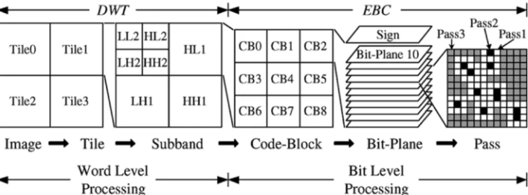
Fig. 1. Decomposition of an image into various abstract levels. These abstract levels include tiles, subbands, code-blocks, bit-planes, and coding passes.
Fig. 2. Output order of DWT coefficients. Although the order of the coefficients within a subband varies with the input scan order, the colocated coefficients in all subbands are always generated consequently.
concurrently. As a result of the stripe pipeline scheduling, the memory requirements are reduced to only 8.5% compared with conventional architectures for 256 256 tile.
This paper is organized as follows. Section II reviews the JPEG 2000 for the description that follows. The proposed ar-chitecture is described in Section III. In Section IV, implemen-tation results are given and are compared with state-of-the-art JPEG 2000 architectures. Section V summaries this paper.
II. JPEG 2000
In this section, we will briefly review the JPEG 2000 coding system, especially the dataflow. Fig. 1 shows how an image is decomposed into abstract levels, which include tiles, subbands, code-blocks, bit-planes, and coding passes. The original image is partitioned into several rectangular tiles, which are indepen-dently coded. The DWT decomposes a tile into levels. Except for the th level that has four subbands, each level has three subbands, including the HL, LH, and HH bands. In general, the DWT coefficients colocated at each subband are generated con-sequently. Fig. 2 shows an example of an 8 8 tile. Each circle represents a DWT coefficient, and the number within the circle indicates the order it is generated. The order of the DWT coeffi-cients generated within each subband depends on the scan order of the DWT engine. However, the colocated DWT coefficients are always generated consequently.
For the EBC, each subband is further partitioned into code-blocks. The DWT coefficients of a code-block are
sign-magni-Fig. 3. Block diagram of the EBC algorithm. It is a context-based arithmetic encoder. The context formation generates the context for the arithmetic encoder to adapt the probability of the decision.
Fig. 4. Procedure of interval subdividing and renormalization. After coding a symbol,A is updated by one of the subintervals, i.e., Q and A 0 Q , and the renormalization is triggered whenever the updatedA is too small.
tude represented and are processed in a bit-plane by bit-plane manner, from the most significant bit plane to the LSB bit-plane. Every bit-plane has three coding passes called Pass 1, Pass 2, and Pass 3. A special coding order called stripe scan is used within any coding pass. A stripe is an 4 rectangle, where is the width of the code-block. The coefficients are scanned stripe by stripe from top to bottom in a coding pass, and column by column from left to right in a stripe.
The EBC is a context-adaptive arithmetic encoder (AE), as shown in Fig. 3. The context formation generates the context-de-cision pair of a sample coefficient according to the coding states of the sample coefficient itself and its eight-connected neigh-bors. The AE is an adaptive, binary MQ-coder. The MQ-coder is a Q-coder [21] that is enhanced by a conditional exchange procedure derived from the MELCODE [22] and the state-tran-sition table known as JPEG-FA [7]. The encoding process of the AE is an iteratively subdividing process of an interval, as shown in Fig. 4. The interval is divided into two subintervals
and , and its base is indicated by . The value of is adapted by the context, denoted by . Each subinterval cor-responds to a symbol, which can be either 0 or 1. The larger one is called the most probable symbol (MPS) while the other is the least probable symbol (LPS). According to the symbol, and are updated. A renormalization procedure is called whenever
is smaller than a specific value. The bit stream is a pointer to the final interval. For more detailed operations of the context for-mation and the arithmetic encoder, the reader is referred to [6].
III. SYSTEMARCHITECTURE
In this section, the proposed JPEG 2000 architecture is pre-sented. The block diagram of the architecture is shown in Fig. 5. Seven stripe buffers (SBs) are used for the stripe pipeline sched-uling; each buffer has 256 11 bits. The LS-DWT generates 256 coefficients for each subband at every pipeline stage. The resulting coefficients are stored in the SBs, and then processed by the CS-EBC.
A. Stripe Pipeline Scheduling
In this section, a stripe pipeline scheduling for JPEG 2000 is proposed. The key concept is to design a scheduling that can minimize the memory requirement while maintaining reason-able complexity and overhead. As described in Section II, the memory issues are arisen from the mismatch between output dataflow of the DWT and the input scan order of the EBC. The mismatch can be solved by using a buffer between the two mod-ules. In conventional architectures [8]–[11], the whole tile and several code-blocks are buffered. Wu et al. [19] proposed a quad code-block (QCB) scheduling scheme that reduces the memory requirements to 1/4 tile and six code-blocks. They also propose a modified QCB scheme [20] to support large tile size. However, the memory requirements are still too high. The proposed stripe pipeline scheduling can fully eliminate the use of tile memory and code-block memory.
An example of the stripe pipeline scheduling is shown in Fig. 6. It is an example for a 256 256 tile with three de-composition levels and for 64 64 code-block. Each rectangle represents a pipeline stage of the scheduling, which is a com-putation state of either the LS-DWT or the CS-EBC. The state of LS-DWT is indicated by, for example, , which means that the LS-DWT is generating left half of the th row to the th row in the th level of the th tile. On the other hand, the state of CS-EBC is indicated by, for example, , which means that the CS-EBC is processing the th stripe of the th code-block to the th code-block of the th tile. The order of execution is from top to bottom. All the com-putation states require 768 cycles except when the CS-EBC is at state, which needs 1024 cycles. In fact, the cycles required in each state are, actually, the number of DWT coefficients that the CS-EBC must encode.
The superiority of the stripe pipeline scheduling lies in that it greatly reduces the data lifetime between the DWT and the EBC. In conventional tile pipeline scheduling, the coefficients trans-formed by the DWT are encoded by the EBC until the transfor-mation of the entire tile is finished. Therefore, the data lifetime equals the processing time of the DWT for a tile. As can be seen in Fig. 6, the data lifetime of the stripe pipeline scheduling is the processing time of a pipeline stage. For the example shown in Fig. 6, the data lifetime is reduced from 256 256 (one tile) to 256 4 (four stripes). Moreover, the reduction rate increases as the increase of tile size. This is because the data lifetime of the tile pipeline scheduling is proportional to the square of tile width, while that of the stripe pipeline scheduling is proportional to tile width only. The memory requirement is also greatly re-duced since it is approximately proportional to data lifetime.
For the stripe pipeline schedule, seven stripe buffers are required as shown in Fig. 5. Each stripe buffer is 256 11 bits, where 11 is the bit-width of a DWT coefficient. While the LS-DWT is writing coefficients into SB-LH0, SB-HL0, and SB-HH0, the CS-EBC is reading coefficients from SB-LH1, SB-HL1, and SB-HH1, or vice versa. When the LS-DWT is processing or the CS-EBC is processing , SB-LL must be accessed by the corresponding module. Therefore, the proposed scheduling only requires about 2.4 KB or 1.75 Kwords (KW) memory, equivalently.
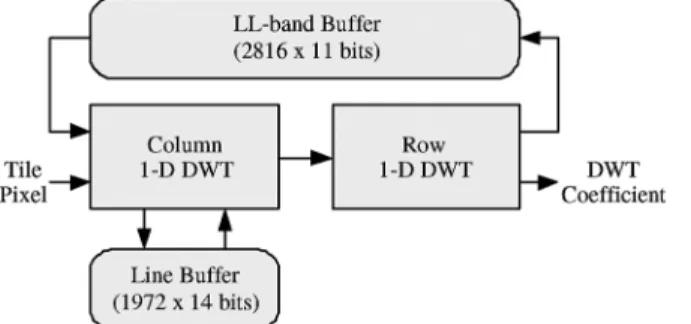
B. Level Switch DWT
In this section, an LS-DWT architecture is proposed. It can greatly reduce the memory requirements of the DWT in JPEG 2000. Fig. 7 shows the architecture of the LS-DWT. It has four major parts, including the two 1-D DWT cores, the line-buffer, and the LL-band buffer. The LL-band buffer stores the LL-band coefficients of lower levels for the decomposition of higher level. In order to switch among different levels with efficient memory usage, the line-based implementation [23] combined with nonoverlapped stripe-based scan [24] is adopted. In the following, the dataflow and memory requirement of the adopted line-based scheme for 2-D decomposition is presented, and the memory requirement for level switch is analyzed. In the fol-lowing analyses, the 2-D DWT is accomplished in column-first order to be compatible with JPEG 2000.
1) 2-D Architecture: Fig. 8 shows a generic line-based 2-D
DWT architecture in column-first order. The line buffer con-tains the data buffer and temporal buffer. The size of the data buffer depends on the scheduling of 1-D column and row DWT.
Fig. 6. Stripe pipeline scheduling. The LS-DWT and CS-EBC are pipelined at stripe level, and therefore the buffer size is reduced to the same as the stripe size. The cycles of a pipeline stage are the coefficients to be processed by the CS-EBC.
Fig. 7. Block diagram of the proposed LS-DWT. It can accomplish multilevel decomposition by two 1-D DWT core.
At the extreme case that row DWT starts after complete column filtering, the size of the data buffer is the same as the tile size. To reduce the size of the data buffer, row DWT must start as
Fig. 8. Generic line-based 2-D DWT architecture. The line buffer contains data buffer and temporal buffer.
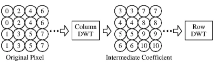
soon as possible to reduce the lifetime of intermediate coeffi-cients. Fig. 9 shows the data flow of the adopted nonoverlapped
Fig. 10. Lifting-based implementation of 9-7 filter for line-based column DWT. It requires four intrinsic registers.
stripe-based scan in the line-based DWT. Each circle represents either a pixel or an intermediate coefficient between 1-D column and row DWT module. The numbers indicate in which cycle the coefficients are scanned. The intermediate coefficients are gen-erated right after the colocated original pixels are scanned. For example, the two coefficients denoted by 3 and 4 in the first column are generated when pixels denoted by 0 are scanned. Thus, only eight registers are required to buffer the interme-diate coefficients. Therefore, the data buffer is eliminated with the nonoverlapped stripe-based scan.
Because the nonoverlapped stripe-based scan requires that the column DWT switch among columns, the intrinsic registers in-side column DWT should also be buffered. This is the temporal buffer depicted in Fig. 8. Fig. 10 shows the lifting-based archi-tecture for 1-D DWT [25], [26] for 9-7 filter. There are four intrinsic registers in this case, and therefore the size of the tem-poral buffer equals to four lines of the tile. Assume that the tile width is 256 pixels: the temporal buffer is
words.
2) Memory Requirement for LS-DWT: In order to reduce
the memory bandwidth and computational complexity, the in-termediate data stored in line-buffer must be buffered when the LS-DWT switches to the next level. Thus, the DWT can con-tinue its operation seamlessly after it switches back to the pre-vious level. For level-switch DWT with decomposition levels, the line-buffer requirement
words, where is the tile width and 9-7 filter is as-sumed. For example, for three-level DWT, the line buffer size . Therefore, it requires 3136 bytes for the line buffer since the coefficient is 14 b in the proposed architecture.
Since is the input of (l 1)th level DWT, the coefficients in LL-band have to be buffered in preparation for the next de-composition level. In conventional architectures, all the coef-ficients in LL-band are buffered since they start the decompo-sition of next level after the finishing of previous level. In the proposed architecture, the LS-DWT can switch to the next level
is the width of the corresponding LL-band. In the proposed architecture, the bit-width of the coefficients is 11 b and the number of decomposition levels is three with 256 256 tile. Thus, the memory requirement for all LL-bands is
. Therefore, the total memory requirement for the proposed three-level LS-DWT is about 7 KB.
C. Code-Block Switch EBC
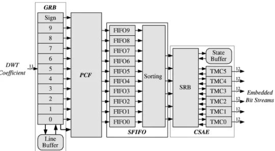
In this section, the architecture of the CS-EBC is described. The block diagram of the CS-EBC is shown in Fig. 11. It comprises four functional modules: the Gobang register bank (GRB), the parallel context formation (PCF), the sorting first-in-first-out (SFIFO), and the code-block switch arithmetic encoder (CSAE). The CS-EBC is based on the parallel EBC architecture proposed in [17] and [18] and is evolved to increase the throughput and to support the code-block switch function. In the following, we will describe the modules in more detail except the PCF module, which is exactly the same as the one in the parallel EBC architecture.
1) Gobang Register Bank: There is only one difference
be-tween the GRB module in the CS-EBC and the one in the par-allel EBC, which lies in the word length of the line buffer. In order to switch among 13 code-blocks, the line buffer is lengthened for 13 code-blocks. The number of words becomes for 13 code-blocks. Although processing 13 code-blocks at the same time, there is only one code-block active in a cycle. Therefore, only one memory is required. Due to the nature of SRAM, the area of a 704 12 single port SRAM is only about three times the area of a 64 12 one, which is much smaller than the ratio 11 of the words of SRAMs.
2) Sorting First-In-First-Out: The reason to use an FIFO in
the CS-EBC is the same as that in the parallel EBC, which is to solve the problem of instantaneous mismatch of throughputs be-tween the PCF and the CSAE. However, their goals are different. In the parallel EBC, a cost-effective architecture is the major de-sign goal. On the other hand, high throughput is the major dede-sign goal for the CS-EBC. Thus, the sorting first-in-first-out (SFIFO) is proposed, which is composed of ten FIFOs and a sorting module. All the FIFOs have six registers. The sorting module selects six FIFOs, which contain the most context and decision (CXD)] pairs, for the six MQ-coders. The RFIFO proposed in [17] and [18] restricts the th MQ-coder to only process CXD pairs from the th bit-plane and the (9 )th bit-plane. Thus, it sometimes happens that some FIFO may be full, which results in stall of the whole system, while some MQ-coders are available. By using the sorting module, it is guaranteed that no stalls would
Fig. 11. Block diagram of the CS-EBC. It can process a DWT coefficient in a cycle, and process 13 code-blocks at the same time.
Fig. 12. Block diagram of the CSAE module. By use of the state buffer and the state register bank, it can concurrently process bit streams of 13 code-blocks.
occur unless all the MQ-coders are busy. The sorting module is realized by the merging networks [27].
3) Code-Block Switch Arithmetic Encoder: In order to
support code-block switch, we proposed a CSAE as shown in Fig. 12. It contains three parts, including the state register bank (SRB), the state buffer, and the six two-symbol MQ coders (TMCs). The state buffer stores the coding state registers for bit streams that are currently processed. The memory requirements for a magnitude bit-plane is 399 b. Thus, a code-block with ten magnitude bit-planes requires 3990 b. Therefore, total memory requirement is 51 870 b since 13 code-blocks are processed in parallel in the proposed architecture.
The SRB has two main functions. First, it acts as the register bank for the TMCs. It provides proper coding states according to parameters from the SFIFO and writes back the coding results from the TMC. Secondly, it reads the coding states of the next code-block to be processed from the state buffer and writes the coding states of the previous code-block back to the state buffer. Each RB has two sets of state registers, each set containing 400 bit registers, for ping-pong mode operation, one for the TMC and the other one for the load/store. There are 256 cycles for the SRB to complete the load/store since each stripe spends 256 cycles. Thus, the minimal bandwidth requirement is
bits per cycle. Therefore, the bitwidth of the
Fig. 13. Block diagram of the TMC module. It always encodes two symbols per cycle.
bus is decided as 16 bit when two-port memory is used. Under this configuration, the register bank for load/store is configured as 25 16-b shift registers. During the load/store, read data and write data are shifted in and out concurrently. The load/store of the ten RBs performs one by one. Therefore, it takes 250 cycles to complete the load/store for a code-block, which is very close to the allotted time, 256.
The configuration of the SRB is the result of compromise between the hardware complexity and the power consumption. At the extreme case of low hardware complexity, all the registers can be connected as a long shift register bank containing 250 registers. However, this scheme will consume very high power since all the registers are active at every cycle. On the other hand, low power consumption can be achieved by using a 250-to-1
Fig. 14. Directly concatenating two-symbol code update module. It is obtained by concatenating two one-symbol code update modules, in which the circuits in gray are for the first symbol and the circuits in white are for the second symbol. The critical path is drawn by dashed lines.
Fig. 15. Architecture of the two-symbol code update module. The second Update C module is in parallel with the first byte output module by modifying the first bit stuffing module to reduce the critical path that drawn by dashed lines.
multiplexer and a counter. By using the counter to control the multiplexer, only one register is read and written in each cycle. Thus, power consumption can be greatly reduced. However, the hardware complexity and the delay are too high. In the proposed SRB, registers in one bit-plane are grouped as a shift register bank. Thus, there are ten shift register banks. Each time, only a shift register bank is active. The power consumption can be greatly reduced since only 25 registers are active instead of 250 registers in the one shift register bank scheme. Moreover, only a 10-to-1 multiplexer and a four-bit counter are required, which are much simpler than the scheme that does not use shift register bank.
There are two special cases for the operations of the SRB. In the first case, no loading is required when the code-block is coded for the first time. In this case, the registers are reset to spe-cific initial values. The other case happens when the code-block is finished, and therefore the state registers are no longer re-quired to store back to the state buffer. Instead, flush is rere-quired to finalize the bit streams. Thus, a small flush circuit, as shown
TABLE I
MEMORYREQUIREMENTCOMPARISON FOR2562 256 TILEWITHTHREE
DECOMPOSITIONLEVELS AND THECODE-BLOCKSIZEASSUMED TOBE
642 64. THECOLUMNDENOTED BYTILE512 IS THETOTALMEMORY
REQUIREMENTWHEN THETILESIZEIS5122 512
in Fig. 12, is used for all the bit streams. The flush circuit only requires one cycle to finalize a bit stream, and thus 28 cycles are required for a code-block. Since the flushing can be performed in parallel with the loading of next code-block, no extra cycles are required.
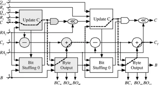
the resulting data path still meets the system timing constraint. Fig. 14 shows the two-symbol code update module by directly concatenating two code update modules proposed in [28]. The circuits in gray are for the first symbol, and the ones in white are for the second symbol. In Fig. 14, the Update C module up-dates according to the range (either MPS or LPS) coded in the interval update stage. is the renormalization amount calcu-lated in the interval update stage. The Bit Stuffing 0 module per-forms bit stuffing and generates a zero mask to remove the bits that has been outputted in . The Byte Output module generates the output bit streams and the corresponding control signals . The critical path, drawn by dashed lines in Fig. 14, of this architecture includes the first Update C module, the first byte output module, the first adder, the second Update C module, the second Byte Output module, and the second adder. Although the above two-symbol code update module seems trivial, the ar-chitecture is much faster than two-symbol arar-chitecture by di-rectly concatenating two conventional architecture. This is be-cause the Bit Stuffing 0 module and the Update C module in the proposed one symbol code update module are processed par-tially in parallel.
In order to further reduce the critical path, the circuits for the first symbol has been modified to enable more parallel pro-cessing. The final architecture of the two-symbol code update module is shown in Fig. 15. The Bit Stuffing 1 module is modified from the original Bit Stuffing 0 module to enable two-step zero masking. At the first step, bits in are removed as if there is only one byte outputted . Thus, the second Update C module can be processed in parallel with the first Byte Output module. However, there will be a wrong bit if the first Byte Output module outputs two bytes. The shifter andXORgate in gray are used to solve this problem. As can be seen in Fig. 15, the critical path, drawn by dashed lines, now includes the two Update C modules, theXORgate, the multiplexer, the second Byte Output module, and the second adder, which is shorter than the architecture shown in Fig. 14. Since there is no pipeline between the interval update module and the code update module, the overall critical path starts from the interval module. However, it is not as long as one may consider, because the code update of the first symbol only depends on the result of the interval update of the first symbol. Therefore, the overall critical path will be that of the code update module plus the interval update for the first symbol.
IV. EXPERIMENTALRESULTS
A. Memory Reduction
To show the performance on memory reduction of the pro-posed stripe pipeline scheduling, we compare the memory requirements for DWT coefficients between the DWT and the EBC in various architectures. The memory requirements de-pends on the specification of the architecture. Without loss of generality, we assume that the tile size is 256 256 and the
Fig. 16. Path delay of the proposed TMC architecture and the conventional architecture. As a result of the proposed techniques, the critical path has been reduced from 22 to 16 ns without extra hardware.
TABLE II
HARDWARECOST OF THEPROPOSEDARCHITECTURE
code-block size is 64 64. The memory requirements of var-ious architectures are shown in Table I. In this table, memory requirements within the DWT and the EBC are not shown since the scheduling will only affect the tile memory requirements. In Table I, the Tile column is the memory size for storing DWT coefficients and the CB column is the code-block memory for the EBC. The DWT column and the EBC column are the additional memory requirements for the DWT and the EBC to support the stripe pipeline scheduling. The numbers in the last column are the total memory requirements if the tile size is 512 512. By the table, the memory requirements are reduced to only 8.5% compared with Amphion’s architecture [8] and 18.8% compared with Wu’s architecture [19], [20] when the tile size is 256 256.
There is another important advantage of the proposed stripe pipeline scheduling: the memory requirements are proportional to the square-root of the tile size while memory requirements of conventional architectures are proportional to the tile size. Therefore, the savings ratio increases with the increase of tile size. As can be seen from Table I, the memory requirement of the proposed architecture is only 4.6% of Amphion’s architecture [8] for 512 512 tile while it is 8.5% for 256 256 tile.
B. TMC Architecture
In order to show the effectiveness of the proposed parallel techniques described in Section III-C3, the proposed TMC ar-chitecture and the conventional arar-chitecture have been synthe-sized with UMC 0.18 cell library. The two architectures have been synthesized by loose timing constraint to exclude the influence of the synthesis variation. The gate counts of the two architecture are almost the same. The conventional two-symbol architecture is obtained by cascading two conventional one-symbol architectures [29]. The distribution of path delay is shown in Fig. 16. The critical path has been reduced from 22 to
16 ns by the proposed techniques. Note that the proposed tech-niques reduce the critical path without the increase of hardware cost.
C. Implementation
The proposed architecture has been described by the Ver-ilog HDL and synthesized with Artisan UMC 0.18 m cell li-brary. The hardware costs are summarized in Table II. This architecture can operate at 124 MHz, which is capable of en-coding HDTV 1920 1080 4:2:2 at 30 frames per second (fps) in real-time. The total logic gate counts are 243 792 gates (in two-input NAND gate equivalent) and the overall memory re-quirement is 133.25 Kb. The tile size can be up to 256 256 and the code-block size can be up to 64 64. The memory for DWT is composed of two 448 28 SRAMs, ten 256 11 SRAMs, and two 128 11 SRAMs. The Stripe Buffer has seven 256 11 SRAMs and the memory for the GRB module is a 704 12 SRAM. All the above memory has been carefully designed to be able to use the single-port SRAM. This has the advantage of low power consumption. On the other hand, the memory for the CSAE is a two-port 3264 16 SRAM since it is inevitable to use two-port SRAM.
The experimental results about the required computation cy-cles are not shown here since the number of cycy-cles is exactly the same as the number of samples to be encoded. Four stan-dard test images—Lena, Baboon, Jet, and Pepper—are exam-ined, and the processing cycles are all the same with the samples to be coded.
D. Comparison
In this section, the proposed architecture is compared with the other architectures. Table III lists the hardware cost as well as the specifications of various architectures. Although the pro-posed architecture needs more logic gates, the memory require-ment is only 33% of others. According to the implerequire-mentation results in [15], the silicon area occupied by memory is about half of the whole design. Thus, the resulting silicon area of the posed architecture will be smaller than others. However, the pro-posed architecture achieves highest throughput/frequency ratio. The memory reduction comes from the proposed stripe pipeline scheduling. On the other hand, the throughput increase is the re-sult of increasing throughput of the arithmetic encoder with the overhead of more logic gate counts.
V. CONCLUSION
In this paper, a memory efficient JPEG 2000 architecture with stripe pipeline scheduling is proposed. The stripe pipeline scheduling takes the throughputs and dataflows of the DWT and the EBC into joint consideration. By matching the throughputs and dataflows of both modules, the tile memory is replaced by the stripe memory with additional memory requirements in the DWT module and in the EBC module. The overall memory requirements are reduced to only 8.5% of the conventional architectures. To support the stripe pipeline scheduling, the LS-DWT and the CS-EBC are proposed. With small additional memory, the LS-DWT can process multilevel in an interleaved order and the CS-EBC can process 13 code-blocks in parallel. The proposed architecture is suitable for large tile size since its memory requirements are proportional to the square-root of the tile size. Moreover, the throughput of the proposed architecture is also increased by the proposed high-speed two-symbol AE architecture. Thus, the proposed architecture has the highest throughput compared with other designs in the literature. When operating at 124 MHz, it can encode HDTV 1920p video at 30 fps in real-time. Therefore, the proposed architecture solves not only the high cost problem but also the low throughput problem for designing a JPEG 2000 encoder.
REFERENCES
[1] Y.-W. Chang, H.-C. Fang, and L.-G. Chen, “High performance two-symbol arithmetic encoder in JPEG-2000,” in IEEE Int. Symp. Consum.
Electron., Sept. 2004, pp. 101–104.
[2] H.-C. Fang, Y.-W. Chang, C.-C. Cheng, C.-C. Chen, and L.-G. Chen, “Memory efficient JPEG 2000 architecture with stripe pipeline scheme,” in IEEE Int. Conf. Acoust., Speech, Signal Process., Philadel-phia, PA, Mar. 2005, vol. 5, pp. 1–4.
[3] JPEG 2000 Part I: Final Draft International Standard (ISO/IEC
FDIS15444-1), ISO/IEC JTC1/SC29/WG1 N1855, Aug. 2000.
[4] D. Taubman and M. Marchellin, JPEG2000: Image Compression
Fundamentals, Standards and Practice. Norwell, MA: Kluwer Academic, 2002.
[5] A. Skodras, C. Christopoulos, and T. Ebrahimi, “The JPEG 2000 still image compression standard,” IEEE Signal Process. Mag., vol. 18, pp. 36–58, Sep. 2001.
[6] D. Taubman, “High performance scalable image compression with EBCOT,” IEEE Trans. Image Process., vol. 9, pp. 1158–1170, Jul. 2000.
[7] JPEG: Still Image Data Compression StandardW. Pennebaker and J. Mitchell. New York, Van Nostrand Reinhold, 1992.
[8] AMPHION, Oct. 2002, CS6510 [Online]. Available: http://www.am-phion.com/cs6510.html
[9] DSPworx, Mar. 2002, Cheetah [Online]. Available: http://www.dsp-worx.com/cheetah.htm
[10] Alma Technologies, Oct. 2002, JPEG2K E [Online]. Available: http:// www.alma-tech.com/
compression with 30 frames/s for digital camera applications,” in IEEE
Int. Solid-State Circuits Conf. Dig. Tech. Papers, San Francisco, CA,
Feb. 2003, pp. 46–47.
[14] H. Yamauchi, K. Mochizuki, K. Taketa, T. Watanabe, T. Mori, Y. Mat-suda, Y. Matsushita, A. Kobayashi, and S. Okada, “A 14402 1080 pixels 30 frames/s motion-JPEG2000 codec for hd movie transmis-sion,” in IEEE Int. Solid-State Circuits Conf. Dig. Tech. Papers, San Francisco, CA, Feb. 2004, pp. 326–327.
[15] H.-C. Fang, Y.-W. Chang, T.-C. Wang, C.-T. Huang, and L.-G. Chen, “High performance jpeg 2000 encoder with rate distortion optimiza-tion,” IEEE Trans. Multimedia, to be published.
[16] L. Liu, N. Chen, H. Meng, L. Zhang, Z. Wang, and H. Chen, “A vlsi architecture of jpeg2000 encoder,” IEEE J. Solid-State Circuits, vol. 39, pp. 2032–2040, Nov. 2004.
[17] H.-C. Fang, T.-C. Wang, C.-J. Lian, T.-H. Chang, and L.-G. Chen, “High speed memory efficient EBCOT architecture for JPEG2000,” in
Proc. IEEE Int. Symp. Circuits. Syst., Bangkok, Thailand, May 2003,
vol. 2, pp. 736–739.
[18] H.-C. Fang, Y.-W. Chang, T.-C. Wang, C.-J. Lian, and L.-G. Chen, “Parallel EBCOT architecture for JPEG 2000,” IEEE Trans. Circuits
Syst. Video Technol., vol. 15, pp. 1086–1097, Sep. 2005.
[19] B.-F. Wu and C.-F. Lin, “Analysis and architecture design for high per-formance JPEG2000 coprocessor,” in Proc. IEEE Int. Symp. Circuits.
Syst., Vancouver, BC, Canada, May 2004, vol. 2, pp. 225–228.
[20] ——, “A low memory QCB-based DWT for jpeg2000 coprocessor supporting large tile size,” in IEEE Int. Conf. Acoust., Speech, Signal
Process., Philadelphia, PA, Mar. 2005, vol. 5, pp. 9–12.
[21] J.-L. Mitchell and W.-B. Pennebaker, “Software implementation of the Q-coder,” IBM J. Res. Develop., vol. 32, no. 6, pp. 753–774, Nov. 1988. [22] F. Ono, S. Kino, M. Yoshida, and T. Kimura, “Bi-level image coding with MELCODE-comparison of block type code and arithmetic type code,” in Proc. IEEE Global Telecommun. Conf., 1989, pp. 255–260. [23] C. Chrysafis and A. Ortega, “Line-based reduced memory, wavelet
image compression,” IEEE Trans. Image Process., vol. 9, pp. 378–389, Mar. 2000.
[24] C.-T. Huang, P.-C. Tseng, and L.-G. Chen, “Memory analysis and ar-chitecture for two-dimensional discrete wavelet transform,” in IEEE
Int. Conf. Acoust., Speech, Signal Process., Montreal, QC, Canada,
May 2004, vol. 5, pp. 13–16.
[25] W. Sweldens, “The lifting scheme: A custom-design construction of biorthogonal wavelets,” Appl. Comput. Harmon. Anal., vol. 3, no. 15, pp. 186–200, 1996.
[26] C.-T. Huang, P.-C. Tseng, and L.-G. Chen, “Flipping structure: an ef-ficient VLSI architecture for lifting-based discrete wavelet transform,”
IEEE Trans. Signal Process., vol. 52, pp. 1080–1089, Apr. 2004.
[27] K. E. Batcher, “Sorting networks and their applications,” in Proc.
AFIPS Spring Joint Comput. Conf., Akron, OH, 1968, pp. 307–314.
[28] H.-C. Fang, Y.-W. Chang, T.-C. Wang, C.-J. Lian, and L.-G. Chen, “Parallel EBCOT architecture for JPEG 2000,” IEEE Trans. Circuits
Syst. Video Technol., vol. 15, pp. 1086–1097, Sep. 2005.
[29] C.-J. Lian, K.-F. Chen, H.-H. Chen, and L.-G. Chen, “Analysis and architecture design of block-coding engine for EBCOT in JPEG 2000,”
IEEE Trans. Circuits Syst. Video Technol., vol. 13, pp. 219–230, Mar.
2003.
Hung-Chi Fang was born in I-Lan, Taiwan, R.O.C., in 1979. He received the B.S. degree in electrical en-gineering and the Ph.D. degree from National Taiwan University, Taiwan, in 2001 and 2005, respectively.
In 2005, he was a Visiting Student at Princeton University, supported by the Graduate Students Study Abroad Program of the National Science Council, Taiwan. He is currently a Senior Engineer with MediaTek Inc., Hsinchu, Taiwan. His research interests are VLSI design and implementation for signal processing systems, image processing systems, and video compression systems.
coding system JPEG 2000, JBIG2, and related VLSI designs.
Chih-Chi Cheng was born in Taipei, Taiwan, R.O.C., in 1982. He received the B.S. degree in electrical engineering from National Taiwan Univer-sity, Taipei, Taiwan, in 2004, where he is currently pursuing the Ph.D. degree in the Graduate Institute of Electronics Engineering.
His research interests include algorithm and archi-tecture for image/video signal processing, discrete wavelet transform, and intelligent video processing.
Liang-Gee Chen (S’84–M’86–SM’94–F’01) was born in Yun-Lin, Taiwan, R.O.C., in 1956. He received the B.S., M.S., and Ph.D. degrees in electrical engineering from National Cheng Kung University, Tainan, Taiwan, in 1979, 1981, and 1986, respectively.
He was an Instructor (1981–1986) and an As-sociate Professor (1986–1988) in the Department of Electrical Engineering, National Cheng Kung University. In the military service during 1987 to 1988, he was an Associate Professor in the Institute of Resource Management, Defense Management College. In 1988, he joined the Department of Electrical Engineering, National Taiwan University (NTU). During 1993 to 1994, he was a Visiting Consultant with the DSP Research Department, AT&T Bell Labs, Murray Hill, NJ. In 1997, he was a Visiting Scholar in the Department of Electrical Engineering, University of Washington, Seattle. During 2001 to 2004, he was the first Director of the Graduate Institute of Electronics Engineering (GIEE), NTU. Currently, he is a Professor in the Department of Electrical Engineering and GIEE, NTU, Taipei, Taiwan. He is also Director of the Electronics Research and Service Organization, Industrial Technology Research Institute, Hsinchu, Taiwan. His current research interests are digital signal-processing architecture design, video processor design, and video coding systems. He has been Associate Editor of the Journal of Circuits,
Systems, and Signal Processing since 1999 and a Guest Editor for the Journal of Video Signal Processing Systems.
Dr. Chen is a member of Phi Tan Phi. He has been an Associate Editor of the IEEE TRANSACTIONS ONCIRCUITS ANDSYSTEMS FORVIDEOTECHNOLOGY
since 1996, as Associate Editor of the IEEE TRANSACTIONS ONVLSI SYSTEMS
since 1999, and an Associate Editor of the IEEE TRANSACTIONS ONCIRCUITS ANDSYSTEMS—II: ANALOG ANDDIGITALSIGNALPROCESSINGsince 2000. He is also an Associate Editor of the PROCEEDINGS OF THEIEEE. He was Gen-eral Chairman of the 7th VLSI Design/CAD Symposium in 1995 and of the 1999 IEEE Workshop on Signal Processing Systems: Design and Implementa-tion. He is the Past Chair of the Taipei Chapter of the IEEE Circuits and Sys-tems (CAS) Society. He is a member of the IEEE CAS Technical Committee of VLSI Systems and Applications, the Technical Committee of Visual Signal Pro-cessing and Communications, and the IEEE Signal ProPro-cessing Technical Com-mittee of Design and Implementation of SP Systems. He is the Chair-Elect of the IEEE CAS Technical Committee on Multimedia Systems and Applications. During 2001–2002, he was a Distinguished Lecturer of the IEEE CAS Society. He received the Best Paper Award from the R.O.C. Computer Society in 1990 and 1994. Annually from 1991 to 1999, he received Long-Term (Acer) Paper Awards. In 1992, he received the Best Paper Award of the 1992 Asia-Pacific Conference on Circuits and Systems in the VLSI design track. In 1993, he re-ceived the Annual Paper Award of the Chinese Engineer Society. In 1996 and 2000, he received the Outstanding Research Award from the National Science Council. In 2000, he received the Dragon Excellence Award from Acer.
![Fig. 14 shows the two-symbol code update module by directly concatenating two code update modules proposed in [28]](https://thumb-ap.123doks.com/thumbv2/9libinfo/8856718.244069/8.891.455.826.98.321/symbol-update-module-directly-concatenating-update-modules-proposed.webp)
