INTRODUCTION
As interconnect feature size decreases and clock frequencies increase, the on-chip resistance-capaci-tance (RC) time delays become the major limitation in achieving faster circuit speeds. In order to reduce the time delays, the use of low-resistivity and low di-electric constant materials is a way to limit the in-terconnect RC time delays for ULSI metallizations.
Copper is the most attractive interconnect for fu-ture devices because Cu has an electrical bulk resis-tivity of 1.7 ⍀ cm and better electromigration re-sistance compared with aluminum alloys.1However, the use of copper has some challenges, such as the lack of a stable self-passivating copper oxide, poor adhesion to dielectric materials, and diffusion of Cu into substrates.2–4 Therefore, the use of diffusion barriers between Cu and the underlying substrate is required.5–7 Hydrogen silsesquioxane (HSQ), with the general formula (HSiO3/2)2n, n ⫽ 2, 3, 4 . . . etc.,8,9has many advantages such as low dielectric constant (k about 2.7), carbon-free, nonetchback processing, excellent gap-filling, good planarization, and low moisture uptake, and is a potential low k material for ULSI application.
Tantalum is an attractive barrier metal in many applications because of its good electrical conductiv-ity, high melting point, and chemical inertness.10It was reported that a Ta barrier layer prevented the
diffusion of Cu into Si substrates11and affected the texture and grain size of deposited Cu, which are critical factors in determining electromigration reli-ability.5,11
In this work, the influence of an underlying bar-rier Ta on the electromigration of Cu deposited on HSQ and SiO2substrates was investigated. The ki-netics of electromigration damage (EMD) are stud-ied by an isothermal resistance change analysis method using the empirical formula2,12,13
dR/dt * 1/R0⫽ AJnexp (⫺Q/kT) (1) The activation energy Q for EMD and the exponent n of the current density are calculated and dis-cussed.
EXPERIMENTAL PROCEDURES
Four-inch diameter p-type (100) Si wafers with nominal resistivity of 1–10⍀ cm were used as sub-strates. After standard RCA cleaning, 50 nm ther-mal oxide was grown at 950°C in a steam atmosphere on some Si substrates. Hydrogen silsesquioxane (HSQ) was prepared by spin-coating Dow Corning Flowable Oxide (FOX-15) on the cleaned Si wafer. The dispense-and-spread cycle was carried out at 500 rpm for 5 sec, and the final ramp cycle was 2000 rpm for 20 sec. The wafers were baked sequentially at 150°C, 200°C, and 300°C for 1 min each on three hot plates.
Journal of ELECTRONIC MATERIALS, Vol. 31, No. 5, 2002 Regular Issue Paper
Barrier Layer Effect of Tantalum on the Electromigration in
Sputtered Copper Films on Hydrogen Silsesguioxane and SiO
2
WEN-LI SUNG and BI-SHIOU CHIOUDepartment of Electronics Engineering and Institute of Electronics, National Chiao Tung Univer-sity, Hsinchu, Taiwan
As IC devices scale down to the submicron level, the resistance-capacitance (RC) time delays are the limitation to circuit speed. A solution is to use low di-electric constant materials and low resistivity materials. In this work, the in-fluence of underlying barrier Ta on the electromigration (EM) of Cu on hydro-gen silsesquioxane (HSQ) and SiO2substrates was investigated. The presence of a Ta barrier not only improves the adhesion between Cu and dielectrics, but also enhances the crystallinity of Cu film and improves the Cu electromigra-tion resistance. The activaelectromigra-tion energy obtained suggests a grain boundary mi-gration mechanism and the current exponent calculated indicates the Joule heating effect.
Key words: Cu-low k dielectric, electromigration, barrier layer, metallization
reliability
(Received November 1, 2001; accepted January 8, 2002)
Sputtered Copper Films on Hydrogen Silsesguioxane and SiO2 473
Curing (completely imidized) HSQ was performed in an N2furnace at 400°C for 1 h. The cured thick-ness of HSQ was about 650 nm. Both the SiO2 -coated and HSQ--coated Si substrates were then processed with conventional photolithography to ob-tain a test pattern. Samples with positive
photore-Fig. 1. The XRD patterns of (a) Ta film on SiO2and HSQ substrates, (b) Cu/Ta films on SiO2, and (c) Cu/Ta films on HSQ. Annealing con-dition: 400°C for 1 h.
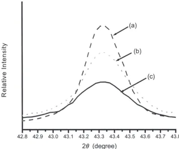
Fig. 2. The Cu (111) peak of (a) Cu/Ta/SiO2/Si, (b) Cu/Ta/HSQ/Si, and (c) Cu/SiO2/Si.
Fig. 3. The SIMS depth profiles of (a) HSQ/Cu/HSQ/Si structure and (b) HSQ/Cu/Ta/HSQ/Si structure, both annealed at 400°C for 1 h.
474 Sung and Chiou
sist patterns were transferred to a vacuum chamber for the sputtering of Ta and Cu films.
High-purity Ar gas was introduced through a mass flow controller after the vacuum chamber was evacuated to about 10⫺6torr. The flow rate of argon was 24 sccm. The sputtering targets were 99.99% Cu disc and 99.95% Ta disc. Before deposition, the target was presputtered for 10 min to remove any contaminate. The gas pressure was kept at 7.6 ⫻ 10⫺3 torr and the sputtering power employed dur-ing deposition was 150 W for Ta and 200 W for Cu. The deposition rates are 0.03 nm/s and 0.14 nm/s for Ta and Cu, respectively. Copper film was sput-tered after Ta deposition without breaking the vac-uum. The film thicknesses were 300 nm copper and 10 nm Ta. The lift-off process was carried out after the sputtering of Ta and Cu to pattern for the EMD test. TEOS films, deposited by the decomposition of tetraethyl orthosilicate, 500 nm in thickness, were deposited onto Cu films with PECVD at 250°C and 100 mtorr.
Conventional photolithography was used to de-fine the contact hole through the TEOS SiO2. Blan-ket Al was then deposited on the specimen for the EM test by thermal coater, which was followed by photolithography. The solution of H3PO4:HNO3: CH3COOH:H2O ⫽ 50:2:10:9 was used to etch ex-cess Al. Samples were then annealed in N2 ambi-ent at 400°C for 1 h.
X-ray diffraction (XRD) was used to examine the metal films phase structure. A field emission scan-ning electron microscope was used to observe the surface morphology and microstructure. An atomic force microscope was employed to measure the sur-face morphology and roughness. A secondary ion mass spectrometer (SIMS) was employed to analyze elemental depth profiles.
The adhesion strength of Cu deposited on HSQ is evaluated with a direct pull tester. A stud was bonded perpendicularly to the coating surface with epoxy by holding it in contact through a spring mounting chip designed especially for the stud. The assembly was cured at 150°C for 1 h. The tester pulled the stud and samples down against the platen support ridge until the coating failed. The stress of adhesion,a(kg/mm2), is defined as a ⫽ F/A. The area of A is the circular section of the stud. The electromigration tests were carried out in a quartz tube at temperatures ranging from 200°C to 300°C in air atmosphere. The four I/O pads of the samples were connected to a constant current source and a microvoltage meter.
RESULTS AND DISCUSSION
The XRD patterns are shown in Fig. 1. There is no new compound formation detected in the XRD pat-terns. The -Ta (200) peak (2 ⬃ 33.7°) is not visible after the deposition of Cu films. On -Ta, the growth of Cu (111) is preferred. A comparison of the Cu (111) peak (2 ⬃ 43.3°) among the Cu film on SiO2, Cu/Ta film on SiO2, and Cu/Ta film on HSQ, shown
in Fig. 2, suggests that the presence of the Ta inter-layer improves the crystallinity of Cu film. The de-gree of crystallinity of Cu/Ta on SiO2is better than that of Cu/Ta on HSQ. The scanning electron mi-croscopy microstructure does not reveal any appar-ent difference between the surface morphologies of Cu and Cu/Ta films.
The SIMS depth profiles of the HSQ passivated Cu/HSQ and Cu/Ta/HSQ specimens are shown in Fig. 3. On the Ta side of the Ta/HSQ interface, a de-crease in the Si and O concentrations is observed. Nevertheless, the Ta side of the Ta/HSQ interface has a larger concentration of H than does the HSQ side of the Ta/HSQ interface. The H may have been dissociated from HSQ after annealing14and trapped in the Ta film. The H atoms behave as electron scat-terers and the incorporation of H into Ta may raise the resistivity of the Ta film.
The film thicknesses of Ta and Cu are ⬃10 nm and ⬃300 nm, respectively. The resistivity of Ta is larger than that of Cu. Hence, current flow through the Ta film is negligible. The resistivities of Cu on SiO2and Cu/Ta on HSQ are 2.25 ⫾ 0.02 ⍀ cm and 2.26 ⫾ 0.07 ⍀ cm, respectively. The presence of the
Fig. 4. Resistance of Cu/Ta films on (a) HSQ and (b) SiO2as a func-tion of temperature.TCR =
1 R 0
.R −R 0 T−T0
Sputtered Copper Films on Hydrogen Silsesguioxane and SiO2 475
Ta interlayer does not affect the resistivity of the metallization.
On the basis of the SIMS spectra, it is not clear whether 10 nm of Ta film can effectively retard the diffusion of the Cu into the substrate. However, the presence of Ta does improve the adhesion of Cu to substrates. The adhesion strengths of the Cu/SiO2 and Cu/HSQ interfaces are 1.42⫾ 0.25 kg/mm2and 6.97⫾ 1.87 kg/mm2, respectively. The presence of Ta raises the adhesion strength to 31.35⫾ 3.24 kg/mm2 (for Cu/Ta/SiO2) and 16.81 ⫾ 5.01 kg/mm2 (for Cu/Ta/HSQ). Addition of the Ta interlayer greatly enhances the adhesion strength of the interface. It is argued that the enhanced adhesion is due to the het-eroepitaxial growth of Cu on-Ta and the formation of a thin amorphous layer at the Ta/Cu interface.7,15
Since the resistance of metal varies in proportion to temperature, i.e., R2⫽ ␣(T2⫺ T1)⫹ R1, the inter-connect temperature can be monitored by
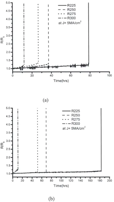
measur-ing the resistance of a test metallization.16Figure 4 gives the resistance of Cu/Ta films on HSQ- and SiO2-coated Si substrates as a function of tempera-ture. During the EMD experiment, the sample tem-perature is obtained from the measured resistance of the test metallization. The relative resistance R/R0as a function of time at various temperatures is shown in Fig. 5. The resistance increases more rap-idly at higher temperatures. By defining a resistance change of 4.5% as the criterion of early stage failure, i.e., assuming the dimensions of the maximum voids are much less than the line width, the time rate change of electrical resistance dR/dt due to electro-migration damage is thermally activated and can be expressed by the following empirical equation:
dR/dt * 1/R0⫽ AJnexp (⫺Q/kT) (1)
Fig. 6. The ln [(dR/dt)(1/R0)] vs. 1/T for Cu/Ta films on (a) HSQ and (b) SiO2during EMD test. Current density: 5 MA/cm2.
Fig. 5. The EMD tests of Cu/Ta films on (a) HSQ and (b) SiO2at a current density J ⫽5 MA/cm2at various testing temperatures.
476 Sung and Chiou
where R0is the initial resistance at a given temper-ature, A is a pre-exponential factor, Jnis the electron current density raised to the nth power, T is temper-ature, and Q is the activation energy for EMD. The activation energies are obtained from the ln [(dR/dt)(1/R0)] vs. 1/T plot shown in Fig. 6 and are 1.1 eV and 1.14 eV for Cu/Ta films on HSQ and SiO2, respectively. Hummel et al. reported that the activa-tion energy for lattice migraactiva-tion in Cu is of the order of 2.3 eV, while that for grain boundary diffusion is about 1.2 eV.17The activation energies obtained sug-gest that lattices are not the major paths for electro-migration in Cu/Ta. Migration via grain boundaries may play an important role in Cu/Ta, because the activation energy for the electromigration of Cu is 0.77 eV.4The Ta barrier layer enhances the migra-tion resistance of copper.
Although the activation energies for the electro-migration of Cu/Ta on HSQ and on SiO2are similar, Cu/Ta films on SiO2have longer EM lifetimes than do those on SiO2, as shown in Fig. 5. Dissociation of H from HSQ, as evidenced from the SIMS depth profile shown in Fig. 3, and diffusion of the impu-rity H into the Cu film may have changed the resis-tivity of the Cu (i.e., Poisson effect) and, conse-quently, resulted in shorter EM lifetime.5 The relative resistance as a function of stress time at various temperatures is shown in Fig. 7a, and the current exponent n in Eq. l, calculated from the EMD data, is 3.21. A current exponent of 2 has been obtained by solving a relatively simple diffusion equation where mass transport due to both concen-tration gradient and electromigration force are treated concurrently.7 Values of n greater than 2 can probably be attributed to Joule heating effects, which result in a temperature gradient-induced flux divergence.
CONCLUSIONS
The barrier effect of Ta on the electromigration of Cu film was investigated. The presence of an ⬃10-nm thick Ta interlayer enhances the adhesion strength of Cu/HSQ and Cu/SiO2 interfaces, al-though the effectiveness in blocking the diffusion of Cu into dielectric is not evident. The activation ener-gies for electromigration failure are 1.10 eV and 1.14 eV for Cu/Ta films on HSQ and SiO2, respec-tively, and suggest a grain boundary diffusion mech-anism. Although no appreciable difference in activa-tion energy is observed, Cu/Ta films on HSQ show shorter EM lifetimes than do those on SiO2. Poison-ing of metallization with hydrogen dissociated from HSQ increases the resistivity of Cu and results in the shorter EM lifetime of specimens on HSQ.
ACKNOWLEDGEMENT
This work is sponsored by the National Science Council, Taiwan, under Contract No. 88-2216-EO09-012.
REFERENCES
1. T. Nitta, T. Ohmi, T. Takewaki, and T. Shibata, J.
Elec-trochem. Soc. 139, 992 (1992).
2. C.K. Hu, B. Luther, F.B. Kaufman, F. Hummel, C. Uzoh, and D.J. Pearson, Thin Solid Films 262, 84 (1995). 3. Y.L. Chin, B.S. Chiou, and W.F. Wu, Jpn. J. Appl. Phys. 39,
6708 (2000).
4. H.W. Wang, B.S. Chiou, and J.S. Jiang, J. Mater. Sci.:
Mater. Electron. 10, 267 (1999).
5. H.Y. Hung and B.S. Chiou, J. Electron. Mater. (in press). 6. H.W. Wang and B.S. Chiou, J. Mater. Sci.: Mater. Electron.
11, 17 (2000).
7. C. Ryu, H. Lee, K.-W. Kwon, A.L.S. Loke, and S.S. Wong,
Solid State Technol. 42, 53 (1999).
8. P.T. Liu, T.C. Chang, Y.L. Yang, Y.F. Chang, F.Y. Shih, J.K. Lee, E. Tsai, and S.M. Sze, Jpn. J. Appl. Phys. 38, 6247 (1999). 9. M.J. Loboda and G.A. Toskey, Solid State Technol. 41, 99
(1998).
10. J.C. Chuang and M.C. Chen, Thin Solid Films 332, 213 (1998).
11. T. Takewaki, H. Yamada, T. Shibata, T. Ohmi, and T. Nitta,
Mater. Chem. Phys. 41, 182 (1995).
Fig. 7. (a) The EMD test of Cu/Ta films on HSQ at 250°C and vari-ous current densities and (b) ln [(dR/dt)(1/R0)] vs. ln J during the EMD test. Temperature: 250°C.
Sputtered Copper Films on Hydrogen Silsesguioxane and SiO2 477
12. R. Rosenberg and L. Berenhaum, Appl. Phys. Lett. 12, 201 (1968).
13. M. Shatzkes and J.R. Lloyd, J. Appl. Phys. 59, 3890 (1986). 14. M.G. Albrecht and C. Blanchette, J. Electrochem. Soc. 145,
4019 (1998).
15. K.W. Kwon, C. Ryu, and R. Sinclair, Appl. Phys. Lett. 71, 3069 (1997).
16. T. Nitta, I. Ohmi, I. Hsohi, S. Sakai, K. Sakaibara, S. Imai, and T. Shibata, J. Electrochem. Soc. 140, 1131 (1993). 17. R.E. Hummel, R.T. Dehoff, and H.J. Geier, J. Phys. Chem.

![Fig. 7. (a) The EMD test of Cu/Ta films on HSQ at 250°C and vari- vari-ous current densities and (b) ln [(dR/dt)(1/R 0 )] vs](https://thumb-ap.123doks.com/thumbv2/9libinfo/7510432.117586/5.918.84.442.88.753/fig-emd-films-hsq-vari-vari-current-densities.webp)
