Evidence for capture of holes into resonant states in boron-doped silicon
S. T. Yen, V. N. Tulupenko, E. S. Cheng, P. K. Chung, C. P. Lee, A. T. Dalakyan, and K. A. Chao
Citation: Journal of Applied Physics 96, 4970 (2004); doi: 10.1063/1.1795985
View online: http://dx.doi.org/10.1063/1.1795985
View Table of Contents: http://scitation.aip.org/content/aip/journal/jap/96/9?ver=pdfcov
Published by the AIP Publishing
Articles you may be interested in
Electron transport and band structure in phosphorus-doped polycrystalline silicon films
J. Appl. Phys. 105, 033715 (2009); 10.1063/1.3068349
Hot hole redistribution in impurity states of boron-doped silicon terahertz emitters
J. Appl. Phys. 98, 093710 (2005); 10.1063/1.2128045
Improvement on electron field emission properties of nanocrystalline diamond films by co-doping of boron and nitrogen
J. Vac. Sci. Technol. B 21, 1074 (2003); 10.1116/1.1576396
Influence of the hole population on the transient reflectivity signal of annealed low-temperature-grown GaAs
Appl. Phys. Lett. 80, 2505 (2002); 10.1063/1.1463209
Calculation of the hole concentration in boron-doped diamond
J. Appl. Phys. 85, 1409 (1999); 10.1063/1.369272
Evidence for capture of holes into resonant states in boron-doped silicon
S. T. Yena)Department of Electronics Engineering, National Chiao Tung University, Hsinchu, 30050 Taiwan V. N. Tulupenko
Department of Electronics Engineering, National Chiao Tung University, Hsinchu 30050, Taiwan and Donbass State Mechanical Engineering Academy, Kramatorsk 343913, Ukraine
E. S. Cheng, P. K. Chung, and C. P. Lee
Department of Electronics Engineering, National Chiao Tung University, Hsinchu 30050, Taiwan A. T. Dalakyan
Department of Electronics Engineering, National Chiao Tung University, Hsinchu 30050 Taiwan and Donbass State Mechanical Engineering Academy, Kramatorsk 343913, Ukraine
K. A. Chao
Department of Physics, Lund University, Sövegutun 14A, S 233 62 Lund, Sweden (Received 17 May 2004; accepted 2 August 2004)
The variation of hole population in the resonant states of B-doped Si excited by sequences of short electric-field pulses has been investigated by the technique of time-resolved step-scan far-infrared spectroscopy. From the variation of the p3/2 absorptions, we find that the hole population in the
ground state decreases continuously with the sequential electric pulses, as a result of the breakdown delay and hole accumulation in long-lived excited states. The measured time-varying spectra of the
p1/2series have been analyzed and attributed to a significant variation of the hole population in the
resonant states. We have also observed a new absorption line at 676 cm−1which is probably caused
by the electric-field induced mixing of the resonant states. © 2004 American Institute of Physics. [DOI: 10.1063/1.1795985]
I. INTRODUCTION
The electronic states of an impurity in semiconductors are regarded as resonant states when they are degenerate in energy with one or more continua of the band structure, a notion originating from Fano.1 One of the most common types of resonant states is the classical one of acceptor states that are associated with the spin-orbit p1/2bands and
degen-erate with the continua of the p3/2 bands in cubic
semicon-ductors. The existence of such resonant acceptor states was first verified by Zwerdling et al. more than four decades ago by observation of the p1/2 excitation spectrum from B- and
Al-doped Si.2 With the advance in techniques of sample preparation and infrared spectroscopy the excitation spectra have been resolved more accurately and reassigned for the
p1/2 resonant states as well as the p3/2 localized states of
various Group III acceptors (B, Al, Ga, and In) in Si.3–6 Theoretical formulations for the resonant states have been developed and so far the calculated results can supply a quantitative interpretation for the measured absorption lines.7,8
Although the problem of resonant states in semiconduc-tors seems not new, the possibility of terahertz 共THz兲 emis-sion in doped semiconductors has renewed interests of re-searchers to it in the last decade since the THz radiation can be connected with the electric-dipole transition from one of the resonant states to a localized state.9,10 The stimulated emission and lasing operation of THz waves have been
real-ized from p type uniaxially deformed Ge with the electric field and the external stress being in parallel10–12and also in crossing13 configurations. The THz gain has been attributed to the population inversion of holes between the resonant states attached to the heavy-hole bands and the localized states attached to the light-hole bands, where the capture of holes from continuous band states into the resonant states plays a key part.9,14Based on an analogous mechanism, pos-sibilities of THz radiation from p-doped strained SiGe(Ref. 15) and quantum wells with resonant impurity states16 have been proposed without the external applied stress. So far, however, there has not yet been any direct experimental evi-dence for the hole capture by the resonant states.
In this paper, we report an experimental evidence for capture of holes into the p1/2resonant states in B-doped sili-con under sufficiently high electric-field pulses. The main idea of the experiment is to observe the time-varying absorp-tions of both the p1/2and p3/2series for B-doped Si excited
by sequences of electric pulses, using the technique of time-resolved (TR) step-scan spectroscopy. This observation can reveal information on the evolution of hole populations in the various types of acceptor states. The reasons for using B-doped Si are as follows. The binding energy of the ground state of B 共B= 45 meV兲 is the smallest among those of the Group III acceptors in Si, rendering the holes in B-doped Si more likely to be ionized in a moderate electric field at a low temperature. Secondly, the oscillator strength of transitions associated with the p1/2 lines is the largest for B compared
with other Group III species in Si.8Furthermore, the optical phonon energy 共op= 63 meV兲 for Si is larger than the
spin-a)Electronic mail: [email protected]
0021-8979/2004/96(9)/4970/6/$22.00 4970 © 2004 American Institute of Physics
orbit split-off energy共⌬=44 meV兲 between the p1/2and the
p3/2bands. It follows that with a low impurity concentration
and at a low temperature, there is a high probability for the ionized holes to gain sufficient kinetic energy in a high electric field to reach the energy of the resonant states before emitting an optical phonon, as illustrated in the inset of Fig. 1. In this situation the hole distribution in the momentum space will strongly displace from an isotropic one as a con-sequence of cyclic streaming motion in which optical pho-non scattering is predominant.17 The average energy of the holes would be high enough and a considerable amount of holes can have kinetic energy in the range B⬍⬍op so
that they can play parts in the impact ionization of holes from the localized states. It is therefore possible for holes in B-doped Si under an appropriate electric field to achieve an ideal distribution for population inversion in such a way that the distribution function be narrow with its maximum at the energy of the resonant state while the localized states remain depopulated.9,14Naturally, one would expect accumulation of holes in the resonant states through resonance scattering or other paths. Such a picture is difficult to achieve for Si doped with other species of acceptors that have a higher binding energy of holes. It is also hardly possible for p-type Ge that has a large spin-off energy ⌬ because the optical phonon scattering will prevent carriers from gaining enough kinetic energy to reach the energy of the resonant state. For polar semiconductors, strong accoustic phonon interaction would cause the distribution of carriers to be broadening in the mo-mentum space, making them also unfit for the population inversion.
II. EXPERIMENT
The experiment was performed using samples with di-mensions of 6⫻12 mm2cut along the[001] crystallographic
axes from a 0.5 mm thick(100) B-doped Czochralski Si wa-fer of a room-temperature resistivity of 8⍀ cm. The acceptor concentration in the samples is estimated to be about 1.5
⫻1015cm−3.18
Two contacts with area of 6⫻4 mm2 were
made using Al on one surface of the samples, leaving a cen-tral 6⫻4 mm2window for spectroscopic measurement. One of the samples was then treated for Ohmic contacts with annealing at 350° C for 30 min. The I-V curves measured from the sample in a pulse mode ensure that the contacts are Ohmic up to 1000 V. Each of the metallic contacts was then soldered together with a piece of 1⫻18⫻6 mm3copper
us-ing pure indium to improve the coolus-ing efficiency of the sample in exchange gas of the continuous flow cryostat. Spe-cial design and tools were used to keep the indium thickness of being 0.45 mm. One of the copper holders was fixed to the finger of the cryostat while the other was left free. Such a scheme of making contacts and fixing the sample was used to alleviate the Joule heating and possible mechanical strain in Si. Rapid-scan spectra with resolution of 2.5 cm−1 were taken from the sample in the aforementioned scheme and from another one mounted to the cryostat finger with a thin teflon film. No difference was found between the spectra in the absence of electric fields.
The cryostat with the sample was put into an IFS66v/S Fourier transform infrared (FTIR) spectrometer in such a way that the sample was capable of being irradiated by light from the FTIR source through the window between the con-tacts. In front of the sample was put symmetrically a screen with a 5⫻2.5 mm2 hole, made of stainless foil covered by black paper to prevent the light from passing through the boundary sides into the sample. A He-cooled Si bolometer was used as a detector. Equipped with a polyethylene filter, a Mylar-3.5m beam splitter, and KRS5 windows for the cry-ostat, the spectrometer allows one to measure spectra of in-terest in the range from 240 to 685 cm−1.
To avoid overheating of the sample the electric field was applied in the burst mode. There were 50 pulses in a burst. The pulse duration was 0.2s and the duty cycle was 0.01. The duration of each burst is thus 1 ms. The repetition rate of the bursts was 15.6 Hz. The Joule heating by the pulses led to a moderate increase in the environmental temperature from a temperature T0 (measured in the absence of electric
fields) to a higher temperature T*. These temperatures were registered by a Ge thermoresistor with a time constant of 100 ms mounted on one of the copper pieces.
To increase the signal-to-noise ratio, 100 sets of data were recorded and coadded for each interferogram using the TR step-scan technique. There were 884 points in the inter-ferogram demanded for an optical resolution of 2.5 cm−1and a phase resolution of 15 cm−1. These parameters were a con-sequence of compromise between the resolution for distin-guishing the absorption lines of interest and the time con-sumption for the measurement. Just before starting a real ac coupled TR measurement, we took a quick dc coupled TR interferogram in the absence of electric fields for further phase correction of the measured AC spectra. The obtained single-channel TR spectra⌬S共, t兲 were further processed to get the corresponding delta absorbance spectra⌬A according to the formula
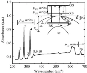
FIG. 1. The absorption spectrum for boron in silicon taken in the absence of external fields at 20 K. The inset illustrates the hole excitation and accelera-tion by the electric field, the hole capture into the resonant states, and the transitions for the p1/2and p3/2absorptions, where the abbreviations GS, XR,
and RS stand for the ground states, the localized excited states, and the resonant states, respectively, of acceptors.
J. Appl. Phys., Vol. 96, No. 9, 1 November 2004 Yenet al. 4971
⌬A共,t兲 = − ln
冋
1 +⌬S共,t兲S0共兲
册
, 共1兲where S0共兲, serving as a reference, is the ac coupled
rapid-scan single-channel spectrum measured at T* but in the ab-sence of electric fields.
III. RESULTS AND DISCUSSION
The absorption line 2p
⬘
and lines 1, 2, 3, and 4(in no-tation of Onton et al.3 ) which are of main interest in the present work can be well resolved. Figure 1 shows the spec-tra measured at 20 K in the absence of electric fields. The positions of the lines are in agreement with the data of Ontonet al.3
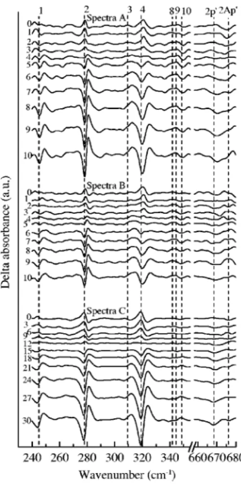
We took three sets, A, B, and C, of electroabsorption spectra in the experiment. In Table I Iare listed some of the parameters adopted for measuring the three sets of spectra, such as the temperatures T0and T*, the applied voltage V, the
electric field E, and the time resolution⌬. The other param-eters which are not listed, such as the pulse width共0.2s兲, the duty cycle (0.01), and the number of pulses (50) in a burst, are the same for the three sets of spectra. The period of time slices at which the data were taken is set to equal the time resolution⌬. We took⌬= 40s for spectra A and B, and 20s for spectra C. It should be pointed out that in spite of the very short time duration ⌬ compared with the time constant 共⬃1 ms兲 of the bolometer, the high sensitivity of the bolometer and the wide dynamic range of a 16-bit analog-to-digital converter in FTIR allow us to observe the variation of optical signals with the time slices. The resulting electroabsorption spectra are shown in Fig. 2, where we show from the two sets A and B the spectra recorded at the first 11 time slices(slices 0–10) but from the set C the spec-tra at the first 11 each-third time slices(slices 0,3,6, ... ,30). Here, each of the first time slices, labeled with 0, was syn-chronized with the beginning of the bursts. We can see from the spectra that the values of delta absorbance ⌬A of p3/2 lines 1 (at 245 cm−1), 2 (at 278 cm−1), and 4 (at 319 cm−1)
are positive at the first several slices(slices 0–3 for spectra
A and B and slices 0 – 9 for spectra C). This means that the
absorptions measured at the first several time slices are larger than the reference absorption measured at T* in the absence
of electric fields. The larger absorption may be attributed to a higher concentration NG of holes in the ground state or a
lower concentration NLX of holes in the localized excited
states since the absorption is proportional to the difference
NG− NLX for the optical transition from the ground state to
the localized excited states. As will be demonstrated later, the lattice temperature TL is dropping during the initial time
slices as well as before the beginning of the bursts. This temperature dropping increases NGwhile reduces NLXbefore
the first electric pulse is applied. The successive electric pulses can then remove holes from the localized acceptor states to shallower ones or to the continuous band states. Holes bound to shallower states are more likely ionized through either the Zener tunneling or the impact process when the electric field is applied. Only a smaller fraction of holes from the deeper ground state are excited by each of the short pulses of electric fields (E=1850, 1300, and 1250 V / cm for spectra A, B, and C, respectively) due to the large separation in energy from the excited states.19 As a consequence, at the initial time slices when the free hole concentration p is small and thus the hole capture from the continuous band states is neglected, more holes are removed from a shallower acceptor state than from a deeper one by the electric pulses. The argument described above can also be supported by the difference in the magnitude of the delta absorbance of lines 1, 2, and 4 at the first time slices, where ⌬A4⬎⌬A2⬎⌬A1(⌬Aibeing the delta absorbance of line i).
It is also a common feature of the spectra that the p3/2
absorptions of lines 1, 2, and 4 decrease monotonically with the time slices. While this may be due to the increase in the lattice temperature TL caused by the Joule heating of the
sequential electric pulses, a further investigation of the tem-TABLE I. Some of parameters for three sets A, B, and C of spectra: the
temperature共T0兲 in the absence of electric fields, the average temperature
共T*兲, the applied voltage 共V兲, the electric field 共E兲, and the time resolution
共⌬兲. The other parameters such as the pulse width 共0.2s兲, the duty circle (0.01), and the number of pulses in a burst (50) are the same for the three sets of spectra.
Spectra T0共K兲 T*共K兲 V共V兲 E共V/cm兲 ⌬共s兲
A 20 27 740 1850 40
B 24 27 530 1300 40
C 45 53 500 1250 20
FIG. 2. The three sets, A, B, and C, of electroabsorption spectra taken at different time slices for boron in silicon excited by sequential electric-field pulses. The parameters for the three sets of spectra are listed in Table I.
perature variation with time slices rules out the simple inter-pretation. In fact, TL drops rather than rises during the first
time slices, since there are a small amount of free holes available to generate Joule heating. This is also evident from Fig. 3(a) where the temporal variation of the delta absor-bance at 605 cm−1was recorded from spectra C. The
absorp-tion at 605 cm−1has been known as the lattice absorption of
bulk Si associated with the process of absorption of a photon and emission of two phonons 共TA+TO兲.20 Such a mul-tiphonon absorption increases with TLrising. With the aid of
the temperature dependence of the absorption at 605 cm−1, we can read from Fig. 3(a), in spite of the small signal-to-noise ratio, that the lattice temperature for spectra C still dropped during the initial 300s(corresponding to the first 15 time slices) but then rised until the temporal point ap-proximately at 1250s which is 250s after the end of the bursts. The lag of the TL variation to the switching of electric-field heating is obviously caused by the lower heat generation rate compared with the rate of heat drained by the cryostat. We expect similar temperature variations for spectra
A and B although a significant variation of the absorption at
605 cm−1 was not observed due to the low temperature
(T0/ T*= 20 K / 27 K and 24 K / 27 K for spectra A and B,
respectively).20 On the basis of the preceding argument, we suggest that the variation of the p3/2absorptions are not
sim-ply dominated by the temperature variation. The decrease in the p3/2absorptions must result mainly from continuous
de-population of the holes in the ground state by the sequential electric-field pulses, accompanied with accumulation of holes in the excited states in the duration between two
near-est pulses. After an electric-field pulse passing, a majority of the excess free holes in the absence of electric fields are captured from continuous band states to localized excited impurity states in a short time and then would cascade to the ground state if the next electric pulse came a sufficiently long time later.21However, the duration between two nearest pulses共20s兲 appears not long enough for the holes to com-plete a transition from the excited to the ground states; oth-erwise, the system would return to a thermal-equilibrium state before the next pulse came and, in this case, the absorp-tion strength would simply be a funcabsorp-tion of temperature only. We conclude that there must exist long-lived (LL) excited states in B-doped silicon so that the hole accumulation in these states occurs in the duration between two nearest pulses. The existence of such long-lived states has also been experimentally confirmed by Lehto and Proctor19 and more recently by Pokrovski et al.22A small fraction of holes in the ground state as well as a majority of the holes in the excited states (including the LL states and other excited states) are then released to the band by the application of the next electric pulse. As a consequence, the ground state popu-lation NGdrops continuously with the time slices while the
concentration p of free holes increases.(The values are av-erage over the time resolution⌬.) Because of the high cap-ture rate of holes from the continuous band states to the excited states, the excited state population NLXis expected to
be strongly related with p; that is, NLX also increases con-tinuously with the time slices. The depopulation of the ground state is more enhanced for a higher electric field and also at a higher temperature, as can be seen from the three sets of absorption spectra A, B, and C. This is because a higher electric field can reduce the breakdown delay and ex-cite more holes from the ground state in the short pulse duration.19 The efficiency of the impact excitation depends also upon the concentration of initial free holes in the con-tinuous band states.19At a higher temperature or at a latter time slice where there are more initial free holes, the popu-lation NG decreases and NLX increases more rapidly. This
explains the more noticeable decrease in delta absorbance of lines 1, 2, and 4 at latter time slices and at a higher tempera-ture (for spectra C). With the picture described, it is not difficult to understand the variations of ⌬A4 and d⌬A4/ dt
with time, as shown in Fig. 3(b). The absorption ⌬A4 first
slightly increases(with positive d⌬A4/ dt) because the effect
of TLdropping dominates over that of the accummulation of
LL holes which then becomes dominant. The heating is more and more important with the time since more and more free holes are available for generating heat. At 250s when the heat generated is balanced with that drained out, TL reaches the minimum, as can be seen from Fig. 3(a). After this time,
TLthen becomes increasing, enhancing the decrease of⌬A4 as can be seen from Fig. 3(b). A very recent observation of THz electroluminescence from B-doped Si can also serve as an additional evidence for the existence of the long-lived excited states and the depopulation of the ground state with successive electric pulses.23
Now let us turn our attention to the p1/2 lines in Fig. 2
(see also Fig. 4 for clarity), which are associated with the electric-dipole transitions from the ground state to the reso-FIG. 3. The delta absorbance(a) for the multiphonon共TA+TO兲 process at
605 cm−1and(b) for line 4 at 319 cm−1as functions of time. Also shown in
panel(b) is the derivative of the delta absorbance for line 4 with respect to time. The data were taken from spectra C at T0= 45 K, T*= 53 K, and E
= 1250 V / cm.
J. Appl. Phys., Vol. 96, No. 9, 1 November 2004 Yenet al. 4973
nant states. The 2p
⬘
line at 668 cm−1 and the 3p⬘
line at693 cm−1have been observed for B-doped Si in the absence
of electric fields,2,3,5while the line marked 2Ap
⬘
at 676 cm−1has never been reported. According to the calculated results of Buczko and Bassani,8there are two energy levels close in energy to the first resonant state ⌫6−; one is the fourfold de-generate level⌫8−located at 0.08 meV(in electronic energy) below⌫6−and the other is a twofold degenerate level ⌫7+at 0.95 meV below ⌫6−. The line 2Ap
⬘
has the wave number associated with the transition from the ground states共⌫8+兲 to the ⌫7+ states, which is nearly forbidden in the absence of electric fields due to the same parity of the envelope func-tions of the⌫8+and⌫7+states.(Note that the total wave func-tions lack a definite parity since the system lacks the inver-sion symmetry.) However, under an electric field applied along the [001] direction, the symmetry of the system re-duces from the Tdgroup to the D2dgroup. Consequently, thethree energy levels of the resonant states⌫6−+⌫7++⌫8−are hy-bridized together and split into four energy levels 2⌫6+ 2⌫7
(⌫6and⌫7 being the irreducible representations of D2d) in a
sufficiently strong electric field. Based on the estimation 具r典eE⬎1.5 meV, where 具r典⬎150 Å is the mean radius of the resonant states8and e the electronic charge, we expect a considerable mixing of the resonant states by the external fields. In this situation, the selection rule is no longer valid and the variation of the 2Ap
⬘
absorption becomes observ-able, as Fig. 2 shows. In contrast to the p3/2absorptions, the p1/2absorptions are smaller at almost all the time slices thanthe reference absorption measured in the absence of electric
fields because of the nonpositive delta absorbance of the p1/2 lines. This means that the TLdropping and the electric fields at the initial time slices do not cause a decrease in the hole population of the resonant states. Instead, the population in the resonant states increases since the negative delta absor-bance of the 2Ap
⬘
line cannot be explained simply by the decrease in the ground state population NG. As has beendescribed previously, NGdecreases during the first time slice
because of the application of the electric pulses. It is an important finding that the negative delta absorbance moves from 2Ap
⬘
to 2p⬘
with the time slices. We attribute the phe-nomenon to a transfer of the excess captured holes from the high-energy resonant state to the low-energy one or probably to the p3/2band states through resonant escape. The negativedelta absorbance of the 2p
⬘
line at latter time slices can be explained by the decrease in the ground state population or the increase in the population of the first resonant state. Such relaxation processes involving the resonant states appear complicated and require further experimental and theoretical investigations for identification.IV. CONCLUSION
In conclusion, we have observed the variations of the hole populations in the ground, resonant, and localized ex-cited states for B-doped Si under trains of electric-field pulses by the technique of TR far-infrared electroabsorption spectroscopy. The ground state population decreases mono-tonically with the successive short electric pulses because of the breakdown delay and the hole accumulation in the long-lived excited states. We have also observed the 2Ap
⬘
absorp-tion line at 676 cm−1 which is believed to be caused by theelectric-field induced mixing of the resonant states. The population of excess holes in the high-energy resonant state has been observed. As time goes on, the holes may transfer to the low-energy state or escape to the continuous band states.
ACKNOWLEDGMENTS
This work was supported by the National Science Coun-cil of the Republic of China under Contract No. NSC 92-2115-E-009-049 and the Swedish Foundation for Interna-tional Cooperation in Research and Higher Education.
1
See, e.g., F. Bassani, G. Iadonisi, and B. Preziosi, Rep. Prog. Phys. 37, 1099(1974).
2
S. Zwerdling, K. J. Button, B. Lax, and L. M. Roth, Phys. Rev. Lett. 4, 173(1960).
3
A. Onton, P. Fisher, and A. K. Ramdas, Phys. Rev. 163, 686(1967).
4
J. J. Rome, R. J. Spry, T. C. Chandler, G. J. Brown, B. C. Covington, and R. J. Harris, Phys. Rev. B 25, 3615(1982).
5
D. W. Fischer and J. J. Rome, Phys. Rev. B 27, 4826(1983).
6
For a review of experimental results obtained up till 1981 on the spectros-copy of acceptors in semiconductors together with the theory for their interpretation, see A. K. Ramdas and S. Rodriguez, Rep. Prog. Phys. 44, 1297(1981).
7
F. Bassani, G. Iadonisi, and B. Preziosi, Phys. Rev. 186, 735(1969).
8
R. Buczko and F. Bassani, Phys. Rev. B 45, 5838(1992).
9
M. A. Odnoblyudov, I. N. Yassievich, M. S. Kagan, Y. M. Galperin, and K. A. Chao, Phys. Rev. Lett. 83, 644(1999).
10
I. V. Altukhov, M. S. Kagan, K. A. Korolev, V. P. Sinis, E. G. Chirkova, M. A. Odnoblyudov, and I. N. Yassievich, JETP 88, 51(1999). FIG. 4. The electroabsorption spectra in the range of large wave number.
The left panel is taken from spectra A and the right panel is taken from spectra C in Fig. 2.
11
I. V. Altukhov, M. S. Kagan, K. A. Korolev, V. P. Sinis, and F. A. Smirnov, Sov. Phys. JETP 74, 404(1992).
12
Y. P. Gousev, et al., Appl. Phys. Lett. 75, 757(1999).
13
V. N. Bondar, A. T. Dalakyan, L. E. Vorob’ev, D. A. Firsov, and V. N. Tulupenko, JETP Lett. 70, 265(1999).
14
M. A. Odnoblyudov, I. N. Yassievich, V. M. Chistyakov, and K. A. Chao, Phys. Rev. B 62, 2486(2000).
15
A. Blom, M. A. Odnoblyudov, H. H. Cheng, I. N. Yassievich, and K. A. Chao, Appl. Phys. Lett. 79, 713(2001).
16
S. T. Yen, Phys. Rev. B 66, 075340(2002).
17
W. E. Pinson and R. Bray, Phys. Rev. 136, A1449(1964).
18
S. M. Sze, Physics of Semiconductor Devices, 2nd ed.(Wiley, New York, 1981), p. 32.
19
A. Lehto and W. G. Proctor, J. Phys. C 11, 2239(1978).
20
F. A. Johnson, Proc. Phys. Soc. London 73, 265(1959).
21
M. Lax, Phys. Rev. 119, 1502(1960).
22
Ya. E. Pokrovski, O. I. Smirnova, and N. A. Khvalkovski, JETP 85, 121 (1997); 90, 404 (2000).
23
T. N. Adam, R. T. Troegger, S. K. Ray, P.-C. Lv, and J. Kolodzey, Appl. Phys. Lett. 83, 1713(2003).
J. Appl. Phys., Vol. 96, No. 9, 1 November 2004 Yenet al. 4975