Effect of void propagation on bump resistance due to electromigration in flip-chip
solder joints using Kelvin structure
Y. W. Chang, T. H. Chiang, and Chih Chen
Citation: Applied Physics Letters 91, 132113 (2007); doi: 10.1063/1.2790376 View online: http://dx.doi.org/10.1063/1.2790376
View Table of Contents: http://scitation.aip.org/content/aip/journal/apl/91/13?ver=pdfcov
Published by the AIP Publishing
Articles you may be interested in
Modeling of electromigration on void propagation at the interface between under bump metallization and intermetallic compound in flip-chip ball grid array solder joints
J. Appl. Phys. 107, 093526 (2010); 10.1063/1.3369442
Morphological evolution of voids by surface drift diffusion driven by the capillary, electromigration, and thermal-stress gradient induced by the steady state heat flow in passivated metallic thin films and flip-chip solder joints. II. Applications
J. Appl. Phys. 104, 023522 (2008); 10.1063/1.2958303
Investigation of void nucleation and propagation during electromigration of flip-chip solder joints using x-ray microscopy
Appl. Phys. Lett. 89, 262106 (2006); 10.1063/1.2425040
Study of void formation due to electromigration in flip-chip solder joints using Kelvin bump probes
Appl. Phys. Lett. 89, 032103 (2006); 10.1063/1.2226989
Effect of three-dimensional current and temperature distributions on void formation and propagation in flip-chip solder joints during electromigration
Appl. Phys. Lett. 89, 022117 (2006); 10.1063/1.2220550
This article is copyrighted as indicated in the article. Reuse of AIP content is subject to the terms at: http://scitation.aip.org/termsconditions. Downloaded to IP: 140.113.38.11 On: Wed, 30 Apr 2014 08:16:44
Effect of void propagation on bump resistance due to electromigration
in flip-chip solder joints using Kelvin structure
Y. W. Chang, T. H. Chiang, and Chih Chena兲
Department of Materials Science and Engineering, National Chiao Tung University, Hsin-chu, 30010 Taiwan, Republic of China
共Received 17 June 2007; accepted 6 September 2007; published online 28 September 2007兲 Three-dimensional modeling is employed to simulate various Kelvin structures for detecting the change in bump resistance due to void formation and propagation during electromigration in flip-chip solder joints. It is found that the Kelvin structures can sense the highest voltage drop when its voltage probes are placed at the current entrance into the bump on the chip side, and it is thus the most sensitive design to monitor void formation and propagation. When the bump resistance increases 20% of its initial value, the depletion percentage of contact opening ranges from 21.0% to 65.0%, depending on the position of the probes. © 2007 American Institute of Physics.
关DOI:10.1063/1.2790376兴
To meet the relentless drive for the miniaturization of portable devices, flip chip technology has been adopted for high-density packaging due to its excellent electrical charac-teristic and superior heat dissipation capability.1 As the re-quired performance in microelectronics devices becomes higher, the operating current continues to increase, which causes the current density to be carried by each solder bump to rise dramatically. Therefore, electromigration has become an inevitably critical reliability issue in flip-chip solder joints.1
Two layouts have been employed to investigate the elec-tromigration behavior in flip-chip solder joints including Daisy chains2and Kelvin structures.3,4Kelvin structures con-stitute four probes, in which two of them are employed to measure the voltage drop across a solder bump. Our previous results show that the change in resistance due to void forma-tion in the initial stage is less than 1 m⍀.4,5In contrast, the typical resistance for a Daisy-chain structure is of the order of a few ohms, while noise from the temperature fluctuation may overwhelm the increase in resistance attributed to the void formation and propagation. Thus, it is less sensitive to void formation or subtle microstructure changes. Therefore, Kelvin structure appears to be a very promising approach to the study of electromigration. It has been implemented in solder joints to monitor the electromigration behavior.3,4,6In addition, geometrical effect of bump resistance measured by Kelvin probes has been investigated experimentally and by simulation.7However, the change in bump resistance due to void propagation is not clear when using different layouts of Kelvin structure.
In this study, three-dimensional finite element analysis was employed to simulate the increase in bump resistance due to void formation using various layouts of Kelvin struc-ture, and some of the simulation results are verified by ex-perimental data. This study provides a fundamental under-standing on how the layout of Kelvin structure affects the measured changes in resistance during electromigration, thus facilitating the study of electromigration study using Kelvin structure.
To examine how the location of Kelvin probes affects the measured resistance of solder bumps, four layouts of Kelvin structure were examined. Figure 1共a兲 shows one of the layouts, which matched the real solder joints with a four-probe Kelvin structure.7The Al trace was 1.5m thick and 100m wide. Eutectic SnPb solder and underbump metalli-zation 共UBM兲 of 0.5m Ti/ 5m Cu/ 3m Ni were
a兲Author to whom correspondence should be addressed. Electronic mail:
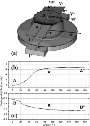
FIG. 1.共a兲 Voltage distribution in the solder joint with a Kelvin structure. The possible positions for the voltage probe on the chip side are also shown in the figure, including 0°, 45°, 90°, and 180°.共b兲 The voltage profile along the A-A⬘-A⬙arc on the chip side.共c兲 The voltage profile along the B-B⬘-B⬙ arc on the substrate side.
APPLIED PHYSICS LETTERS 91, 132113共2007兲
0003-6951/2007/91共13兲/132113/3/$23.00 91, 132113-1 © 2007 American Institute of Physics This article is copyrighted as indicated in the article. Reuse of AIP content is subject to the terms at: http://scitation.aip.org/termsconditions. Downloaded to IP:
adopted. The two probes for applying current and the two probes for sensing the voltage drop are labeled in the figure. The voltage distribution is also shown in the figure with an applied current stress of 0.8 A. To obtain the bump resistance using Kelvin structure, the voltage along the part of the pe-ripheries of the circular Al pad and the Cu pad was extracted. Figures 1共b兲 and 1共c兲show the voltage distributions along the A-A
⬘
-A⬙
arc in the Al pad on the Si side and along theB-B
⬘
-B⬙
arc in the Cu pad on the substrate side, respectively. The voltage ranges from −8.0 to − 1.1 mV along theA-A
⬘
-A⬙
arc of the Al pad, while it varies from 0.25 to 0.67 mV along the B-B⬘
-B⬙
arc of the Cu pad. The voltage distri-butions on the left-hand side of both curves show abrupt changes, which is attributed to the fact that current crowding effect occurs seriously on the left-hand side of the joints.8 The bump resistance Rbumpin this letter is denoted asRbump= ⌬V Itotal =Vtop− Vbottom,max Itotal , 共1兲
where Vtop is the voltage obtained from the top Al pad at a
specific angle, Vbottom,max denotes the maximum voltage
value obtained from the bottom Cu pad, and Itotalis the total
current applied in the simulation model. Since the bump re-sistance was calculated from the voltage drop divided by the applied current, the measured bump resistance is propor-tional to the measured voltage drop.
Since the voltage distributions are not uniform on both Al and Cu pads, the voltage drop detected by Kelvin probes may vary, causing the measured bump resistance to differ with different probe layouts. Furthermore, the voltage varia-tion on the Al pad may exceed 6 mV at different posivaria-tions, whereas it is only less than 0.5 mV on the Cu pad, which means that the position of the voltage probe on the Al pad plays a crucial role on the measured bump resistance. There-fore, only the position of the voltage probe on the Al pad was changed in this study. The position of the voltage probe on the Cu pad was fixed, as shown in Fig.1共a兲.
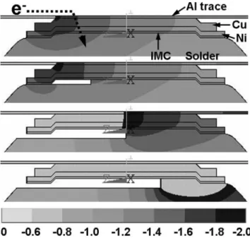
To investigate how void propagation influences bump resistance by simulation, a series of models with various sizes of voids were constructed. Figure2illustrates the cross-sectional view of the solder joints for four of the 29 con-structed models. Pancake-type voids were assumed to propa-gate along the interface between Ni3Sn4 intermetallic compound共IMC兲 and eutectic SnPb solder.9The shape of the void was assumed to be irregular, which is consistent with our previous x-ray results.10The depletion percentage of the UBM opening is 0%, 6.1%, 50.0%, and 75.0%, respectively, for the five models. As voids formed and propagated, more current was forced to drift longer to the right side along the Al pad and the UBM layer, causing the voltage to redistribute.
It is found that different layouts of Kelvin probes detect different increases in resistance even for the same void size. Figure3共a兲depicts the measured voltage drop as a function of depletion percentage of the UBM opening when the volt-age probe was placed at 0°, 45°, 90°, and 180° positions in Fig.1共a兲. The mean voltage at each position was obtained by averaging its neighboring values within 10m. The results indicate that the Kelvin structure detected a higher increase in voltage when the voltage probe was placed at 0°, which was the entrance point of electron flow. For example, when the void depleted 50% of the UBM opening, the increase in voltage detected by the four layouts is 0.97, 0.83, 0.60, and
0.38 mV, respectively. It is concluded that the probe would sense higher changes in voltage when the voltage probe is placed closer to the current crowding region for the same void size. This is because higher current passage will render higher voltage drop for a given increase in resistance. Since there is a current feeding line at position 0°, a voltage probe cannot be fabricated there. Adding the voltage probe on the
FIG. 2. The cross-sectional view for five of the simulation models. The depletion percentage of the UBM opening is共a兲 0%, 共b兲 6%, 共c兲 50%, and 共d兲 75%.
FIG. 3.共a兲 The increase in voltage as a function of depletion percentage of UBM opening with the four different positions of voltage probe on the chip side.共b兲 Percentage increase in bump resistance vs depletion percentage of UBM opening for the four layouts.共c兲 Enlarged illustration for Fig.2共b兲 within 22% increase in bump resistance.
132113-2 Chang, Chiang, and Chen Appl. Phys. Lett. 91, 132113共2007兲
This article is copyrighted as indicated in the article. Reuse of AIP content is subject to the terms at: http://scitation.aip.org/termsconditions. Downloaded to IP: 140.113.38.11 On: Wed, 30 Apr 2014 08:16:44
current feeding line, slightly away from the bump is thus suggested. Although some of the Al-line resistance would be included for the measurement by this layout, it would be the most sensitive method for detecting the change in resistance due to void formation.
Nevertheless, the trend reverses in terms of the percent-age increase in voltpercent-age. Figure 3共b兲 shows the percentage increase in the measured voltage. As the voltage probe moves far away from the current crowding region, the per-centage increase in bump resistance due to the same void size is higher. This is attributed to the fact that the initial bump resistance is much lower as the probe moves away from the current crowding region. The bump resistances are 9.2, 3.5, 0.5, and 0.4 m⍀ for the probes at 0°, 45°, 90°, and 180°, respectively. As voids form, although the probe at po-sition 180° can sense smaller voltage drop than that at 0°, its percentage increase in bump resistance will become higher than that of 0° because it is normalized to its initial resistance.
The above results may provide a better criterion for elec-tromigration failure in the flip-chip solder joints. In Al and Cu interconnects for microelectronic devices, failure crite-rion for electromigration is often defined when their resis-tances reach 1.2 times共20% increase兲 of their initial values. Figure3共c兲shows the magnified figure for the initial stage of electromigration up to 22% increase in resistance in Fig. 3共b兲. When the bump resistance increases 20% of its initial value, the depletion percentage of UBM opening is only 21.0%, 22.0%, 39.0%, and 65.0% with the Kelvin probe measured at 180°, 90°, 45°, and 0°, respectively. However, in most of the recent studies for solder joint electromigration, failure was taken when open-circuit occurred. Moreover, it is reported that degradation of Al trace often takes place at later stages of electromigration of solder joints.11 Damage may also occur in other components rather than the solder bump itself. Therefore, this failure criterion using Kelvin structure may provide a better way to measure mean time to failure, and may thus facilitate the measurement of activation energy for electromigration failure in solder bumps.
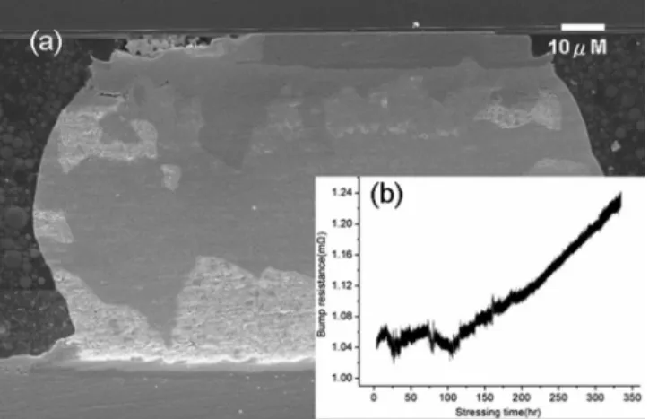
To verify if the simulation results are reliable, experi-mental measurement was also carried out using Kelvin struc-ture with the voltage probes located at 180°. The experimen-tal setup and the joint structure were reported in our previous publications.4,7 Figure 4共a兲 shows the cross-sectional scan-ning electron microscopy 共SEM兲 image for a SnPb bump after the current stressing by 0.9 A at 160 ° C for 334.4 h. The bump resistance increased 18% of its original value after the stressing condition, as shown in Fig.4共b兲. The depletion percentage of UBM opening was estimated to be 37% using the cross-sectional SEM image in Fig. 4. The simulated results in Fig.2共b兲indicate an approximate 28% of depletion percentage共in length兲 for the same increase in bump resis-tance. The two results show reasonable agreement. Neverthe-less, the simulation value appears slightly lower than the experimental one, which may be attributed to that the void shape and area in the simulation models do not match the real ones perfectly. In addition, phase separation and IMC formation would affect bump resistance,12but the simulation did not consider the two microstructural changes.
In summary, effect of void formation and propagation on bump resistance due to electromigration in solder joints has been investigated using Kelvin structures with various lay-outs. The Kelvin structure can sense the highest voltage drop when its voltage probes are positioned at the current entrance into the bump on the chip side. Therefore, Kelvin structures with probes near the current entrance are more sensitive to void formation. In addition, other factors that may influence the effect of void formation on bump resistance need to be studied in the future, such as the dimension and materials of the wiring trace on the chip side, as well as UBM materials and dimension, and the void shape.
The authors would like to thank the National Science Council of the Republic of China for financial support through Grant No. NSC 95-2218-E-009-022. In addition, as-sistance from the simulation facility of the National Center for High-performance Computing 共NCHC兲 in Taiwan is highly appreciated.
1K. N. Tu, J. Appl. Phys. 94, 5451共2003兲.
2A. T. Huang, A. M. Gusak, K. N. Tu, and Y.-S. Lai, Appl. Phys. Lett. 88,
141911共2006兲.
3S. L. Wright, R. Polastre, H. Gan, L. P. Buchwalter, R. Horton, P. S.
Andry, E. Sprogis, C. Patel, C. Tsang, J. Knickerbocker, J. R. Lloyd, A. Sharma, and M. S. Sri-Jayantha, Proceeding of Electronic Components and Technology Conference, IEEE Components, Packaging, and Manufac-turing Technology Society, San Diego, CA, 2006共unpublished兲.
4Y. W. Chang, S. W. Liang, and C. Chen, Appl. Phys. Lett. 89, 032103
共2006兲.
5S. W. Liang, Y. W. Chang, T. L. Shao, C. Chen, and K. N. Tu, Appl. Phys.
Lett. 89, 022117共2006兲.
6S. N. Gee, N. Kelkar, J. Huang, and K. N. Tu, Proceedings of IPACK 2005
ASME InterPACK, San Francisco, CA, USA共unpublished兲.
7S. W. Liang, Y. W. Chang, and C. Chen, J. Electron. Mater. 35, 1647
共2006兲.
8E. C. C. Yeh, W. J. Choi, and K. N. Tu, Appl. Phys. Lett. 80, 580共2002兲. 9L. Zhang, S. Ou, J. Huang, K. N. Tu, S. Gee, and L. Nguyen, Appl. Phys.
Lett. 88, 012106共2006兲.
10S. H. Chiu and C. Chen, Appl. Phys. Lett. 89, 262106共2006兲.
11S. W. Liang, S. H. Chiu, and C. Chen, Appl. Phys. Lett. 90, 082103
共2007兲.
12C. K. Chou, C. A. Chen, S. W. Liang, and C. Chen, J. Appl. Phys. 99,
054502共2006兲.
FIG. 4.共a兲 Cross-sectional SEM image for a SnPb bump after being stressed by 0.9 A at 160 ° C for 334.4 h.共b兲 The corresponding change in resistance as a function of stressing time.
132113-3 Chang, Chiang, and Chen Appl. Phys. Lett. 91, 132113共2007兲
This article is copyrighted as indicated in the article. Reuse of AIP content is subject to the terms at: http://scitation.aip.org/termsconditions. Downloaded to IP: 140.113.38.11 On: Wed, 30 Apr 2014 08:16:44