This content has been downloaded from IOPscience. Please scroll down to see the full text.
Download details:
IP Address: 140.113.38.11
This content was downloaded on 01/05/2014 at 12:31
Please note that terms and conditions apply.
Effect of sputtering power on the structural and optical properties of RF magnetron sputtered
ITO films
View the table of contents for this issue, or go to the journal homepage for more 1994 Semicond. Sci. Technol. 9 1242
(http://iopscience.iop.org/0268-1242/9/6/014)
Effect of sputtering power on
the
structural and optical properties of
RF
magnetron sputtered
ITO
films
Wen-Fa Wu, Bi-Shiou Chiou and Shu-Ta Hsieh
Department of Electronics Engineering and Institute of Electronics, National Chiao Tung University, Hsinchu, Taiwan
Received 5 January 1994, accepted for publication 1 March 1994
Abstract. The structural and optical properties of RF magnetron sputtered ITO films without in situ substrate heating and post-deposition annealing are investigated. The structure and orientation of I T 0 films strongly depends on the energy of t h e sputtered particles arriving at t h e substrate. As the sputtering power increases from 15 to 100 W, the preferred orientation of the ITO film changes from (222) to
(400). It is observed that the lattice constant of the film increases initially as sputtering power increases from 15 to 50 Wand then decreases with further increase of sputtering power. The higher the sputtering power, the smaller the oxygen content of the film. The oxygen deficiency is used to explain the loss of transmittance or blackening of IT0 films deposited at high sputtering power.
Several material parameters, such as optical constants and energy gap, have been derived and discussed. The figure of merit of the films ranges from 81.3 to 117.6 Cl-’.
1. Introduction
Transparent conductive indium tin oxide (ITO) films have been extensively used in a variety of electronics and opto- electronics applications because of their high transmission in the visible range, high infrared reflection and low electrical resistivity [l-SI. ITO films have been deposited by a variety of methods such as sputtering [I-3, 9-22], electron-beam evaporation [S, 6, 23,241, spray pyrolysis
[4,7,25] and screen-printing [26J Magnetron sputtering can deposit films over large areas at rates comparable to electron-beam evaporation without the degree of radiation heating typical of thermal sources. The depo- sition rates ofmagnetron sputtering are higher than those for conventional radio-frequency (RF) sputtering and a
wide range of materials can be deposited [27]. Magnetron sputtering is considered to be one of the best methods for preparing ITO films. High-quality ITO films prepared by magnetron sputtering have been reported [l, 9-15].
Although ITO films with both high electrical con-
ductivity and high visible transmittance can be obtained, the blackening of ITO films was frequently observed
during deposition of ITO films [6, 12, 221 and/or
subsequent sputtering of dielectric films on rro-coated substrates [28-301. This made the transparent conductive
rro
films unstable during operation. Kobayashi et a[, in their work on Iro/silicon oxide/Si junction solar cells, attributed the darkening of ITO to the presence of metal indium [6]. Wu and Chiou [I21 and Matsuoka et al[28] argued that the reduction of SnO, in ITO films resulted 026a-1242/94/061242+06 $19.50 @ 1994 IOP Publishing Ltdin the blackening Of [To. Fan and Goodenough associated
the darkening with the formation of a second phase in the bulk of the films [22]. However, the mechanism for the blackening of ITO films is not clear. In this research,
x-ray photoelectron spectroscopy (XPS) and x-ray diffrac- tion techniques are employed in the study of blackening of ITO films. In addition, the effect of sputtering power
on the structural and optoelectrical properties of the ITO films are investigated and discussed.
2. Experimental details
IT0 fihns were prepared by using a commercial RF magnetron sputtering system (ION TECH, UK). The sputtering target was a 1 in hot-pressed oxide ceramic (90 wt% In,03 and 10 wt% SnO,, 99.99% purity) supplied by Superconductive Components, Inc., USA. The sub- strates employed were made of Corning 0211 glass, degreased ultrasonically in a dilute detergent solution, rinsed ultrasonically in de-ionized water and blown dry in N, gas before they were introduced into the chamber. The substrate was fixed directly above the target with a target-to-substrate distance of 5 cm and a mechanical shutter was attached to the target. The substrate temperature was measured with a thermocouple
in
intimate contact with the substrate.
The vacuum chamber was a stainless steel bell jar pumped by a conventional oil diffusion pump (Diffstak 250, Edwards, UK). High-purity Ar (99.999%) was
Effect of sputtering power on properties of ITO films
introduced through a mass flow controller after the vacuum chamber was evacuated to about 2 x Torr. The gas pressure was monitored with a precision ionization gauge and was kept at 6.5 mTorr during deposition. The RF power (13.56 MHz) was introduced through an RF power supply (RF Plasma Products, Inc.,
USA) with an automatic matching network which could be tuned for minimum reflected power. The sputtering power employed ranged from 15 to 125 W and during sputtering the substrate temperature was between
-
60 "C (15 W) and -90 "C (125 W). Before deposition, the targetwas usually presputtered for 20-30 min to remove any contaminants and eliminate any differential sputtering effects.
Film thickness was measured with a stylus surface profiler. An x-ray diffractometer was used to identify the crystalline phase of the films. Chemical binding energy analysis was performed using an x-ray photoemission spectroscope (XPS; PERKIN PHI-590AM SAM/1905 ESCA, Massachusetts, USA) with an Mg K, x-ray source.
The microstructure of the films was analysed using a scanning electron microscope (SEM; Hitachi S-4000,
Japan). The optical transmittance of the films were measured with an ultraviolet-visible-near-infrared speo trophotometer (Hitachi U-3410, Japan).
3. Results and discussion
Figure 1 gives the x-ray diffraction patterns for the as-deposited ITO films prepared at various sputtering
powers.AIl thepeakscan beassignedtothecubicbixhyite structure of In,03. In the ASTM powder pattern for In,03, the strongest peak is (222) and the third peak is (400) with a relative intensity 1(400)/1(222) of 0.3. In this study, at low sputtering power (P = 15 W), the two peaks (400) and (222) appear prominently, indicating the coexistence of (100) and (11 1) textures. At a power level between 25 and 75 W, the (222) peak disappears and the (400) peak becomes very strong, resulting in a preferred orientation in the (100) direction. However, as the sputtering power increases further, the (222) peak reappears, and the intensity of peak (222) is comparable to that of peak (400) at
P
= 125 W, as summarized intable 1. Kumar and Mansingh, in their work on RF
sputtered ITO films, found that the structure and orienta- tion
of ITO
films depended on the energy of the sputtered particles arriving at the substrate. They suggested that the thermalized sputtered atoms prefer to orientate in the (222) direction and the particles with higher energies prefer the (400) and (440) orientations depending on their energies [17]. Latz et al [l] and Suzuki et al [31]3 (d) 75 watts
3
r
(e) 100 w a t t sFigure 1. X-ray diffraction patterns for the as-deposited [TO films prepared at various sputtering powers
~~ ~~~ ~
28 (degree)
Table 1. X-ray diffraction results for ITO films.
Sputtering Lattice Relative
power cpnstant Strongest intensity
(W) (AI peak /(222)//[400)~ 15 10.173 (222) 1.842 25 10.224 (400) 0.043 50 10.281 (400) Negligible 75 10.258 (400) 0.014 100 10.241 (400) 0.215 125 10.216 (400) 0.987
a In the ASTM powder pattern for ln203, the relative intensity
/(222)//(400) is 3.33.
observed a variation of the orientation from (222) to (400) with an increase in substrate temperature from
-
100 to -300 "C. In the present study, the trend that the preferred orientation of ITO films vanes from (222) to (400) as sputtering power increases from 15 to 75 W is consistent with that reported previously [l, 17, 311. However, further investigation is needed to explain the reappearance of the (222) peak at P>
100 W.The cubic lattice constants, calculated
from
the most prominent peak in the x-ray diffraction patterns, are summarized in table 1. The lattice parameter ranges from 10.173 to 10.281A
as compared with the ASTM value of 10.118 8, for bulk h,03 [3]. There are severalpossibilities which might result in the lattice expansion of the IT0 films. One is the replacement of In3+ ions with Sn2+ ions and/or the incorporation of
Sn
ions in the interstitial positions [3, 111. The radii of the In3+, Sn4+ and Sn2+ ions are 0.79A,
0.69 8, and 0.938,
respectively [32]. The substitution of SnZ+ for In3+ would cause an expansion, as observed in the present study. The lattice constant increases from 10.173 to 10.281 8, as the sputtering power increases from 15 to 50 W and decreases with further increase of sputtering power. The mechanism which causes the increase of lattice parameter atP
<
50 W is yet to be determined. The decrease of latticeconstant with increasing RF power at P
>
50 W can be attributed to the decrease of oxygen content at high sputtering power 021. At high sputtering power, the substrate is being bombarded to a greater extent and the oxygen could be resputtered from the film during film growth. The oxygen is iiberated and pumped off during the deposition process, resulting in a decrease in the oxygen content in the film. The decrease in the oxygen content enhances the presence of oxygen vacancies and results in the contraction of the lattice structure. One other possibility which causes the increase of lattice parameter is the residual stress in the sputtered film. However, further study is needed to reveal the contri- bution of the residual stress to the lattice expansion of the film.Figure 2 gives the average transmittance, averaged over the wavelength range 0.45-0.8 pm, as a function of sputtering power. The average transmittance drops from
SO%
to 67% as the sputtering power increases from 15 to 125 W. XPS measurements were carried out to findchemical bonding states of ITO films and to explore 1244
'""I
!I
20 0 0 50 100 1 Sputtering Power (W) 0 Figure 2. Average transmittance of the as-deposited ITOfilms, averaged over the wavelength range 0.45-0.8 pn, as a function of sputtering power.
the possible mechanisms for the loss
of
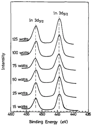
transmittance (or blackening) of ITO films prepared at high power. The In3d, Sn 3d, and 0 1s XPS spectra of the as-deposited ITO films prepared at various sputtering powers are shown in figures 3, 4 and 5 respectively. The position of the
carbon 1s peak is taken as a standard (binding energy = 284.6 ev) to compensate for any charge-induced shifts. The obtained binding energies agree well with the values reported in theliterature [5,21-25,28,33,34]. As shown in figure 3, the observed binding energies of the In 3d,,,
Binding Energy (eV)
Figure 3. in 3d XPS spectra for t h e as-deposited I T 0 films prepared at various sputtering powers.
I---
I
I
500 496 492 488 484 480 BINDING ENERGY (eV)
Figure 4. S n 3d XPS spectra for the as-deposited ITO films
prepared at various sputtering powers.
0 1s
-
I 15 wait
, I
I 536 532 528 524 !
BINDING ENERGY (eV)
Figure 5. 0 1s XPS spectra for the as-deposited ITO films
prepared at various sputtering powers.
and In 3d3/, levels are nearly the same, 444.4 and 452.0 eV respectively, for all samples. Since the extra electronic charge in the ITO films is trapped only at Vo (oxygen
vacancies) and Sn centres, the In 3d3/, and In 3d5,, peaks should be insensitive to the loss of oxygen and to the
Effect of sputtering power on properties of ITO films
Sn concentration [22]. It is reported in the literature
[23,33] that the In 3d peak for metal indium is observed at energies 0.4-1.4eV lower than that for In,03. Kobayashi et al [6] studied the darkening of ITO films
prepared by electron-beam evaporation and suggested that darkening observed for the ITO films can be
attributed to the presence of metal indium. However, no evidence exists in the present study to support the presence of metal indium in these ITO films. There is some
asymmetry of the peaks, indicating that a multiple component may be present. Nelson and Aharoni [34] reported that the XPS In 3d,,, peak can be resolved into
two peaks which are separated by approximately 1.0 eV. The positions of the two resolved peaks in the In 3d,/, spectra are located at 443.7 and 444.6 eV. They suggested that the lower-energy peak located at 443.7 eV corre- sponds to Ino bonding state, specifically In-In bonds, and the higher-energy peak located at 444.6 eV corre- sponds to In3+ bonding state, specifically In,03.
As shown in figure 4, almost the same Sn 3d3,, and Sn 3d5/, spectra are observed for the as-deposited ITO
films prepared at various sputtering powers. Two peaks due to Sn~~3d3!, and Sn 3d,,, are located at 495.0 ? 0.2 and 486.4 & 0.2 eV respectively. Fan and Goodenough [22] reported that the Sn 3d peak for Sn” in SnO is observed at energy 0.5 eV higher than that for Sn” in SnO,, whereas the Sn 3d peak for metal tin is observed at an energy 1.8eV lower than the Sn4+ 3d peak. Thermodynamically SnO, is more stable than SnO and thus Sn4+ is thought to be the predominant state in the
ITO films. Fan and Goodenough suggested that the
darkening of the RF sputtered ITO films was caused by
the formation of the Sn30., phase. However, no evidence for Sn,O,-like phase exists in the present work.
Figure 5 shows the XPS 0 1s spectra of the as- deposited ITO films prepared at various sputtering powers.
A shoulder appears on the higher energy of the main peak for the 0 1s spectra in all samples. All the spectra (except
P
= 25 W) can be resolved into the two peaks at 530.0 and 531.7 eV, as shown by the broken line in figure 5. h,03 crystallizes with a bixbyite C-type cubic rare earth sesquioxide crystal structure with space group TlIa3 [22, 351. Each indium atom is surroundedby six oxygen atoms at the corners of a distorted cube, with two vacancies at the two unoccupied corners. Fan and Goodenough suggested that the lower energy peak located at 530.0 eV corresponds to 0’- ions which have neighbouring In atoms with their full complement of six nearest-neighbour 0’- ions, and the higher energy peak located at 531.7eV corresponds to 0,- ions in an oxygen-deficient region. Nelson and Aharoni proposed another possible explanation for the higher-energy peak and suggested that the higher-energy peak located at 531.7eV may represent the existence of 0-Sn bonds based on other group IV oxides [34]. As shown in figure
5 , the main peak of the 0 Is spectrum shifts to high
binding energies at high sputtering power. It is believed that the magnitude of the shift to higher binding energies should vary with the oxygen deficiency associated with the nearest-neighbour In3+ ions. The 0 Is spectrum
Table 2. XPS compositional analysis of ITO films.
Atomic concentration
(A)
RF power Theoretical (W)
x,
n xs.xo
1.5x,, fw,,
xol~o,,bo,,,t,,> 50 38.6 4.5 56.8 66.9 0.849 100 39.77 4.13 56.1 67.915 0.826 75 38.7 4.5 56.6 67.05 0.844 125 40.0 4.63 55.37 69.26 0.799becomes very broad for the ITO film deposited at 25 W sputtering power, and another peak in addition to the two peaks already mentioned appeared at -534.1 eV, as indicated in figure 5. It is suggested [23] that the 534.1 eV
peak is attributed to oxygen atoms in the InOH species. It results from the existing OH groups on the surfaces of the samples which are caused by interaction with the surfaces of the samples under atmospheric conditions.
Compositional analysis is accomplished by dividing the peak areas by their respective atomic sensitivity factors and thus yields atomic per cent concentrations. Table 2 presents these XPS compositional analyses of 110 Nms deposited at different sputtering powers. This table also contains the theoretical estimate of the oxygen content
(X,
= l.SX,,+
U,,, whereX
indicates atomic per cent) and compares this value with the experimental value. This comparison shows that a lack of oxygen is observed in all samples and the film becomes more non-stoichiometric as the sputtering power is increased during deposition. It suggests that the number of oxygen vacancies increases at high sputtering power and black- ening is caused by the oxygen deficiency in the ITO films. These results agree well with those obtained from the x-ray diffraction experiment mentioned previously.A block diagram of the algorithm for calculating the refractive index n(1) and the extinction coefficient k(%) of
a thin optical layer from the transmission spectrum is shown in figure 6. A detailed description is given as follows.
According to Swanepoel’s method [36], which is based on the idea of Manifacier et al[37] of creating the envelopes of interference maxima and minima in the transmission spectra, an approximate initial value of the refractive index of the film no in the spectral region of medium and weak absorption, can be calculated by the expression (1) where no = [ N
+
( N 2
-
s2)1’2]1’2 T M-
T, S*+
1 N = 2s-+
-.
TM
T, 2Here TM and
T,
are the transmission maximum and the corresponding minimum at a certain wavelengthL,
one being measured and the other calculated; s is the refractive index of the Corning 0211 glass substrate and a value of 1.523 is used. The basic equation for interference fringes is4nd = mA (3)
where m is an even integer for maxima and an odd integer for minima, and d is the film thickness. Film thickness d was measured with a stylus surface profiler. The order of a given extremum ma can be estimated from equation
(3) using d and the corresponding n,. In addition, the
values of m, can be determined by a simple graphical method based on equation (3). This expression can be
rewritten for that purpose as
I = 4 d
t)
- m l (4)where I = O , 1,2
,...
and m 1 is the first extremum. Therefore, plotting I against no/,? yields a straight line with slope 4d and intercept on the y axis of -m,. From this plot the values of m, and hence each correspondingorder of a given extremum ma can be estimated. The orders of m of the neighbouring extrema are in fact
consecutive integers, even for the maxima and odd for the minima of the transmission. The final value of n for each extremum is obtained by substituting film thickness d and the corresponding exact integer values of m
associated with each extreme point in equation (3). The value of the extinction coefficient
k
is obtained by theobtain ~ p e c t r u m T
I
I
Estimate extremum ordem mo
EVeJuate extremum orders m
I
~ Chlcul&te final n
1
I
Compute kI
Figure 6. Block diagram of the algorithm for calculating
n(L) and k(1) of a thin optical layer from t h e transmission spectrum.
following equations (5) (6) x = e x p - - - d . (7) 8n‘s E , = -
+
( n 2 - I)(n’ ~ s’) T, E , - [ E 6-
(n2 - l)’(n2 - s ~ ) ] ~ ’ ~ ( n - l ) 3 ( n-
s2) x = -(
4:1
The refractive index versus wavelength for the ITO
films deposited at different sputtering powers is shown in figure 7. The refractive index of the ITO film decreases
with the wavelength
A,
i.e. dn/dA < 0. This is consistent with what one would expect from Kramers-Kronig analysis [9]. It is seen that the ITO films deposited at high sputtering power have a large value of refractive index. Figure 8 shows SEM micrographs of ITO films preparedat 15 and 125 W. The 125 W deposited ITO film has a smoother and denser structure than does the 15 W deposited one. It is argued that the denser structure is one reason for the larger refractive index of the film. The
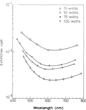
ITO films deposited at higher RF power have larger extinction coefficients, as shown in figure 9.
The transmission in the fundamental absorption region can be expressed by the equation
T z exp( - r d ) (8)
where T is the transmittance, OL is the absorption
coefficient and d is the film thickness. The absorption coefficient r for the direct allowed transition can be written as [IO, 381
(9)
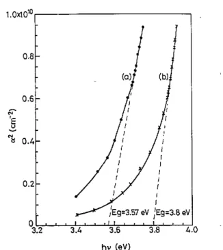
where hv is the photon energy, E, is the transition energy gap and A is a constant. Figure 10 shows the photon energy dependence of 1’ for two 8000
A
thick ITO films1 = A(hv - E 8 ) 1 ’ 2
Effect of sputtering power on properties of ITO films
Figure 8. SEM microstructure of the I T 0 films deposited at (a) 15 W and (b) 125 W .
Wavelength (nm) Wavelength (nm)
Figure 9. Extinction coefficient k versus wavelength for the as-deposited IT0 films prepared at various sputtering powers.
Figure 7. Refractive index n versus wavelength for the as-deposited i ~ o films prepared at various sputtering powers.
Table 3. Comparison of IT0 films prepared by different researchers.
Figure of merit Transmittaace ( x 1 0 - 3 W 1 )
Substrate temperature Sputtering power Sheet resistance (2. = 5500 A),
Reference
.
(“C) (W) R.h(a
0-7
T (%) T”lRsh TIRehPresent work 60 15 10.4 84.56 17.97 81.3
Present work 75 75 6.94 81.63 18.93 117.6
Present work 90 I25 7.15 69.53 3.69 97.3
Latz et a/ [I] 300 600 19 a7 13.1 45.8
Karasawa and Miyata [I61 Near room temperature 15 55 84 3.18 15.2
Ray et a/ [391 370 200 4.5 90 77.5 200
0
hv (eV)
Figure 10. Square of the absorption coefficient a as a function of*photon energy hv for ITO films with a thickness of -8000 A. Sputtering power: (a) 25 W (b) 75 W.
deposited at 25 and 75 W. Extrapolations of the straight regions of the plots to U = 0 give the energy gap
Eg.
TheE , values obtained are 3.57 and 3.8 eV for films prepared
at 25 and 75 W respectively. The carrier concentrations increase with the increasing RF power, they are 2 x
lozo cm-3 and 3 x 1020 cm-’ for films deposited at 25 and 75 W respectively [l2]. Hence a larger energy gap is obtained for films prepared at higher power as predicted by the Burstein-Moss equation [9, 10, 381
where N is carrier concentration, Ego is the intrinsic bandgap, h is Planck‘s constant and m, is the reduced effective mass.
Common to all transparent conductor applications is the need for optimizing the electrical and optical coating parameters. 1deally.both the parameters should be as large as possible but their interrelationship usually excludes the simultaneous achievement of both criteria. To judge the performance of transparent conducting
1248
films, there are several ways to define the figure of merit. In table 3, two common definitions of figure of merit are adopted. The figures of merit for some ITO films prepared in this study are listed together with some of the values obtained by other researchers. The figures of merit of the low-power sputtered ITO films in this study are com-
parable to those reported in the literature. The small figure of merit for films prepared at 125 W is attributed to the blackening of the film.
4. Conclusion
The structural orientation of RF magnetron sputtered ITO
films strongly depends on the sputtering power. Two peaks, (222) and (400), appear prominently in x-ray diffraction patterns of ITO films deposited at 15 W. The (222) peak disappears and the (400) peak becomes predominant as sputtering power increases from 25 to
75 W. The (222) peak reappears and the peak intensity
of the (222) is comparable to the (400) peak at P = 125 W. In the sputtering power range 50 to 125 W,
the lattice parameter of the as-deposited films is smaller for films deposited at higher power. The decrease oflattice parameter is attributed to the increase of oxygen vacancies in the film.
Blackening of ITO Nm is observed for films prepared
at high power.
ws
analyses of the films suggest that the oxygen deficiency results in the loss of transmittance of the films.Sputtering power also affects the optoelectric par- ameters of the ITO films. The higher the sputtering power, the larger the refractive indices and the extinction coefficients. The transition energy gaps of 8000
A
thickITO films are 3.57 and 3.8 eV for films deposited at 15
and 75 W respectively. The figures of merit of the films in this study are comparable to those reported in the literature.
Acknowledgment
This work is supported by the Chung-Shan Institute of Science and Technology (contract no CS 82-0210-D-009- 016) and partly supported by the National Science Council of Taiwan (contract no NSC 82-0417-E009-395).
Effect of sputtering power on properties of ITO films
rZOl Bosnell J R and Waehorne R 1973 ThinSolidFilms 15 141 References
[l] Latz R, Michael K and Scherer M 1991 Japan. J. Appl. Pkvs. 30 L149
[2] Hoheisel M. Mitwalsky A and Mrotzek C 1991 Phys. Status Solidi a 123 461
[3] Fan J C C and Bachner F J 1975 J. Electrochem Soc.
122 1719
[4] Ashok S , Sharma P P and Fonash S J 1980 IEEE Trans. Electron Devices 21 725
[SI
Haga K, Murakami A, Adachi K, Kumano M and Watanabe H 1992 Japan. J. Appl. Phys. 31 925 [6] Kobayashi H, Ishida T, Nakamura K, Nakato Y andTsubomura H 1992 J. A D D ~ . Phvs. 12 5288
[A
Frank G, Kauer E and K6stfih H 1581 ThinSolid Films 77 107[SI
Kido J, Nagai K and Okamoto Y 1993 IEEE Trans.[9] Wu W F and Chion B S 1993 Appl. Surf: Sci 68 497
[lo] ChiouBSandHsiehST1993 ThinSolidFilms229146
[ll] ChiouBS.HsiehSTandWuWF 1994 J.Am.Ceram.Soc.
[12] Wu W F and Chiou B S 1994 Thin Solid Films at press [13] Chiou B S. Hsieh S T and Wu W F 1994 Appl. Sur&
Cl41 Shigesato Y , Takaki S and Haranou T 1991 Appl. S u r j
rl5l Martinez M A, Herrero J and Gutitrrez M T 1992 Sol. Electron Devices 40 1342 at press Sci. at press Sei. 48/49 269
_ _
Energy Mater. 26 309 135[16] Karasawa T and Miyata Y 1993 Thin Solid Films 223 ~~ ~
C171 Kumar C V R V and Mansingh A 1989 J. Appl. Phys.
[18] Tee W-K, Machino T and Sughihara T 1993 Thin Solid
[19] Shigesato Y , Hayashi Y , Masui A and Haranou T 1991 65 1270
Films 224 105
Japan. J. Appl. Phys. 30 814
fZlj Hennig H, HecknerK-H, Hirsch D and Ladwig H
1982 Phvs. Status Solidi a 74 133
[221 Fan J C C &d Goodenough J B 1977 J. Appl. Phys. 48
1 W A
--_
I[23] Ishida T, Kobayashi H and Nakato Y 1993 J. Appl.
Pkur 72 A Z M
I ..I". ," _ _ _ ~ r
[24] Mori N 1993 J. Appl. Phys. 73 1327
[25] Major S, Kumar S , Bhatnagar M and Chopra K L r261 Bessak B. Euaouia H and Bennaceur R 1993
1986 Appl. Phys. Lett. 49 394
_ _
Semicond. Sei. Technoi. 8 1671
[27] Vossen J L and Kern W 1978 Thin Film Process (New York Academic)
[ZS] Matsuoka T, Knwata J, Fujita Y and Abe A 1988
Japan. J. Appl. Phys. 27 L1199 [29] Panicker M P R and Essinger W F 1981
J. Electrochem. Soc. 128 1943
[301 Chubachi Y and Aoyama K 1991 Japan. J. Appl. Phys.
30 1442
[311 Suzuki K, Hashimoto N, Oyama T, Shimizu J, Aka0
Y and Kojima H 1993 Thin Solid Films 226 104 [321 Kingery W D, Bowen H K and Uhlmann D R 1975
Introduction to Ceramics 2nd edn (New York: Wiley) p 85
[33] Hewitt
R
Wand WinogradN
1980 J. Appl. Phys. 51 2620 [34] Nelson A J and Aharoni H 1987 J. Vac. Sci. Tecbnol. A [351 Elfdal I, Pilkington R D and Hill A E 1993 Thin Solid[36] Swanepoel R 1983 J. Phys. E: Sci. Instrum. 16 1214 r371 Manifacier J C. Gasiot J and Fillard J P 1976 J. Phw.
5 231
Films 223 303
- _
E: Sci. Instrum 9 1002
r381 Ohhata Y, Shinoki F and Yoshida S 1979 Thin Solid
_ _
FiIm.59 255
A K 1983 J. Appl. Phys. 54 3497
[391 Ray S, Banerjee R, Basu N, Batabyal A K and Barua