國立交通大學
顯示科技研究所
碩士學位論文
硒化鎘鋅磊晶層的高壓拉曼散射光譜
研究
Raman Spectroscopy Study of Zn
1-x
Cd
x
Se
Epilayers at High Pressure
研究生:吳聲嵩
指導教授:陳志隆 教授
共同指導教授:周武清 教授
硒化鎘鋅磊晶層的高壓拉曼散射光譜研究
Raman Spectroscopy Study of Zn
1-xCd
xSe Epilayers at High Pressure
研 究 生:吳聲嵩 Student:Sheng-Sung Wu
指導教授:陳志隆 老師
Advisor:Jyh-Long Chern
共同指導教授:周武清 老師 Co-advisor:Wu-Ching Chou
國 立 交 通 大 學
顯 示 科 技 研 究 所
碩 士 論 文
A ThesisSubmitted to Institute of Electronics College of Engineering National Chiao Tung University
in partial Fulfillment of the Requirements for the Degree of
Master in
Display Institute
July 2006
Hsinchu, Taiwan, Republic of China
硒化鎘鋅磊晶層的高壓拉曼散射光譜研究
學生:吳聲嵩 指導教授
:陳志隆 教授
共同指導教授
:周武清 教授
國立交通大學顯示科技研究所
摘
要
在本論文中,以微拉曼散射光譜來研究在砷化鎵基板上成長不同鎘含量的 硒化鎘鋅磊晶層的光學特性。實驗發現在室溫、大氣壓力下不同鎘含量的硒化鎘 鋅磊晶層其縱向光學聲子模頻率和橫向光學聲子模頻率會隨著鎘含量的增加而 減少,其強度也有減弱的趨勢。晶格振動模態屬於單模特性。並且利用鑽石高壓 砧的技術,在室溫下觀察不同鎘含量樣品的拉曼譜線隨壓力之變化。我們發現在 對不同鎘含量的硒化鎘鋅其縱、橫向光學聲子模振動頻率會隨壓力增加而變大, 即為有藍位移現象,當壓力加到轉換壓力時,其縱向光學聲子模消失,但橫向光 學聲子模仍然存在,此壓力即為半導體由閃鋅礦結構轉變為岩鹽結構的臨界壓 力。我們發現硒化鎘鋅磊晶層之相位轉變壓力會隨著鎘含量的增加而減少,此現 象 歸 諸 為 鎘 含 量 增 加 而 造 成 的 晶 格 不 穩 定 。 最 後 我 們 也 計 算 聲 子 頻 率 與 Grünesien 參數隨壓力變化的關係。
Raman Spectroscopy Study of Zn
1-xCd
xSe Epilayers at High Pressure
Student:Sheng-Sung Wu Advisor:Prof. Jyh-Long Chern
Co-advisor:Prof. Wu-Ching Chou
Display Institute
National Chiao Tung University
ABSTRACT
In this thesis, Zn1-xCdxSe epilayers of zinc-blende phase were grown on the
GaAs substrates were studied by using micro-Raman scattering experiment. At ambient pressure, two peaks labeled as transverse optical (TO) phonon mode and longitudinal optical (LO) phonon mode are observed for each Zn1-xCdxSe epilayers.
From the Raman spectra, the vibration frequency decreases and the linewidth increases with the Cd concentration. The lattice vibration mode behavior of Zn1-xCdxSe epilayers belongs to the one-mode behavior. The high pressures were
generated by using a diamond anvil cell. For Zn1-xCdxSe epilayers with x = 0.00, 0.06,
0.08, 0.14, 0.25, and 0.32, all Raman peaks blue shifted to higher frequencies when the pressure was increased. As the pressure was increased to the transition pressure, the LO phonon disappeared. The disappearance of the LO phonon in Raman spectra at high pressure is attributed to the semiconductor to metal phase transition. The metallization occurred when the crystal structure transformed from a four-coordinated zinc-blende (ZB) phase into a six-coordinated rock-salt (RS) phase. As x was increased, the semiconductor to metal-transition pressure decreased. The decrease in transition pressure with x implies the decreasing crystal stability with x. Finally, we also calculated the pressure variation of the phonon frequencies and Grünesien parameters of the two optical modes.
ACKNOWLEDGEMENT
轉眼間我在交大兩年的求學生活即將結束。回想兩年的研究所生活充滿 著辛酸和淚水,不過也讓我成長不少,不管是學術研究,還是待人處事方面。 在研究所的兩年來。首先要感謝的是我的父母及家人因為有他們的生活 上的支持與鼓勵使我能夠專心學業。而我能夠順利取得學位最要感謝周武清 教授和陳志隆教授,因為有老師的指導與教誨我才能完成我的論文,特別是 周武清老師在我最需要幫助的時候拉我一把,除了學問上,也告訴我們許多 做人處世的道理,讓我受益匪淺。 還有感謝實驗室的祝壽,謝博,郭博,繼祖,瑞雯,京玉,阿邦,怡仁, 彥丞,瑞泰,還有文忠學長在實驗儀器的操作及生活上給予我的指導與幫助。 還有實驗室同學啟仁,維偲,尚樺,哲豪以及實驗室的學弟妹筱筑,進吉。謝 謝你們的陪伴讓我的研究生活充滿更多的歡笑與回憶。 總之,要感謝的人真的太多了,感謝這幾年來出現在我生命中的所有人, 因為有你們的出現我的生活才會如此的多采多姿。CONTENTS
Page
Abstract (in Chinese)
iAbstract (in English)
iiAcknowledgement
iiiContents
ivList of Figures
vList of Tables
viiChapter 1 : Introduction
1Chapter 2 : Principle of Experiment
32.1 Preparation of Sample 3
2.2 High-pressure Technique 4
2.2-1 Diamond Anvil Cell 4
2.2-2 Pressure Medium 5
2.2-3 Pressure Calibration 5
2.3 Micro-Raman Scattering Experiments 6
2.3-1 The Principle of Raman Scattering 6
2.3-2 Experimental Setup 7
2.4 Experimental Process 8
Chapter 3 : Result and Discussion
153.1 Raman Scattering of Zn1-xCdxSe Epilayers at Atmospheric
Pressure
15 3.2 Raman Scattering of Zn1-xCdxSe Epilayers at High Pressure 17
Chapter 4 : Conclusion
37References
38LIST OF FIGURES
Fig. 2.1 Schematic structure for Zn1-xCdxSe epilayers... ...10
Fig. 2.2 Basic setup of diamond anvil cell...11
Fig. 2.3 Ruby fluorescence verse pressure in a pressure medium of deionized-water. The right-hand and left-hand side peaks of the plots present R1 and R2 peaks of the ruby fluorescence lines, respectively…….... ...12
Fig. 2.4 Energy level of Cr+3 in Al2O3. The transitions of E1/2→A and E3/2→A give rise to R1 and R2 lines, respectively.... ...13
Fig. 2.5 Schematic diagram of Raman scattering experiment. ...14
Fig. 3.1 Raman spectra of Zn1-xCdxSe for x = 0.00, 0.06, 0.08, 0.13, 0.14, 0.25, and 0.32 at ambient pressure...22
Fig. 3.2 Composition dependence of the zone-center optical phonon frequencies in zinc-blende Zn1-xCdxSe...23
Fig. 3.3 Raman spectra of ZnSe at different pressure. ...24
Fig. 3.4 Raman spectra of Zn0.94Cd0.06Se at different pressure ...25
Fig. 3.5 Raman spectra of Zn0.92Cd0.08Se at different pressure ...26
Fig. 3.6 Raman spectra of Zn0.86Cd0.14Se at different pressure ...27
Fig. 3.7 Raman spectra of Zn0.75Cd0.25Se at different pressure ...28
Fig. 3.8 Raman spectra of Zn0.68Cd0.32Se at different pressure ...29
Fig. 3.9 Pressure dependence of LO and TO peaks for ZnSe...30
Fig. 3.11 Pressure dependence of LO and TO peaks for Zn0.92Cd0.08Se ...32
Fig. 3.12 Pressure dependence of LO peak for Zn0.86Cd0.14Se ...33
Fig. 3.13 Pressure dependence of LO peak for Zn0.75Cd0.25Se ...34
Fig. 3.14 Pressure dependence of LO peak for Zn0.68Cd0.32Se ...35
Fig. 3.15 Concentration dependence of transition pressure for Zn1-xCdxSe epilayers...36
LIST OF TABLES
Table 2.1 Growth condition of Zn1-xCdxSe epilayers…...9
Table 3.1 Effect of pressure on various Raman vibrational modes of Zn1-xCdxSe at room temperature. The value of mode
frequenciesωi, pressure dependence i
d dp
ω
, and mode Grünesien parameter γi were obtained at ambient condition…...21
Chapter 1
Introduction
The wide band gap II-VI compound semiconductor family has attracted intense interest for the past decades due to its applications in optoelectronic devices. In particularly, ZnSe-based ternary compound semiconductors, such as Zn1-xCdxSe,
Zn1-xMnxSe, have attracted much attention due to its tunability in lattice constant and
band gap. Among them, Zn1-xCdxSe is one of the most intenerating compounds
because its band gap covers most of visible light region from blue to red. Ternary compound Zn1-xCdxSe was widely used as an active layer in a strained single
Zn1-xCdxSe quantum well with ZnSSe or ZnSe barrier of the II-VI semiconductor
blue-green diode lasers [1, 2, 3]. As a result, the optical and electrical properties of Zn1-xCdxSe epilayers grown by molecular beam epitaxy (MBE) were studied
extensively.
In past decades, several kinds of high pressure studies on III-V and II-VI semiconductors have been performed. Ves et al. investigated the band shift of ZnSe as a function of pressure by transmission experiment [4]. The structure transition from zinc-blende to rock-salt phase was identified by optical absorption experiment. The x-ray diffraction experiments were carried out to observe the structure transformations at high pressure by McMahon et al. [5] and Greene et al. [6]. The resistance measurement revealed metallization process at high pressure of semiconductor [7]. Usually, the semiconductor-metal transition pressure can be identified by the energy-dispersive x-ray diffraction (EDXD) which measures change of crystal structure. It accompanies disappearance of the longitudinal optical (LO) phonon mode in Raman spectra [8]. Hence, the Raman scattering studies under hydrostatic pressure
is a powerful tool to investigate the phase transition of crystal structure of semiconductor materials.
Raman scattering studies at high pressure for III-V and II-VI semiconductors have received much attention in recent year [9, 10, 11]. Recently, the Raman scattering experiments were applied to study the pressure effect on Zn1-xFexSe [8], Zn1-xCoxSe
[12], and Zn1-xMnxSe [13, 14] crystals. To our knowledge, study of Zn1-xCdxSe
epilayers of zinc-blende phase grown by molecular beam epitaxy is rare. In this thesis, the Raman scattering of Zn1-xCdxSe epilayers at room temperature and under
hydrostatic pressure reported.
In Chapter 2, the experimental details of highpressure Raman scattering were described. The experimental results of the lattice vibration of Zn1-xCdxSe epilayers at
high pressure were presented in Chapter 3. Finally, Chapter 4 concludes our experimental results and gives future direction.
Chapter 2
Principle of Experiment
In this chapter, we describe the experimental techniques used in this thesis. The experimental techniques include high-pressure technique, and micro-Raman scattering measurement. The sample preparation which was used in the high-pressure experiment is also presented.
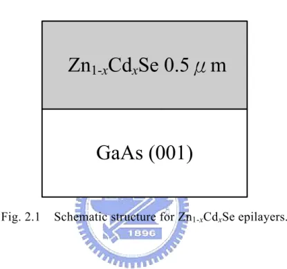
2.1 Preparation of Sample
In this work, the Zn1-xCdxSe epilayers of zinc-blende phase were grown on the
(001) GaAs substrates using the Veeco Applied EPI 620 molecular beam epitaxy system. The GaAs substrate was mounted on molybdenum disk holder by Indium. After the substrate holder was loaded on the transfer rod in the introduction chamber. We turned on the oil free diaphragmpump and the turbo pump. When the introduction chamber’s pressure is below 10-8 torr, we open the manual gate valve and transfer the substrate holder (molybdenum disk) to the growth chamber by the substrate transfer arm. The substrate temperature was raised up to 650 oC for removing the oxide on the GaAs substrate. After clear RHEED pattern was observed, the substrate temperature was decreased to 300 oC for growing the Zn1-xCdxSe epilayers. For the Zn1-xCdxSe
epilayers, the cell temperatures of Zn and Cd were ranged from 300 oC to 260oC and from 230 oC to 210 oC, respectively. While, the cell temperature of Se was fixed at 175
o
C. The substrate temperatures were set at 300 oC. Under the above growth conditions, the growth rate of 0.35 Å/s was obtained. The structures of Zn1-xCdxSe epilayers were
0.5 μm. The growth parameters of the Zn1-xCdxSe epilayers were shown in Table 2-1.
2.2 High-pressure Technique
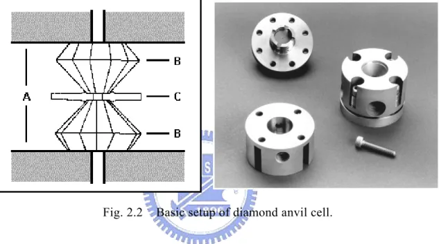
2.2-1 Diamond Anvil Cell
The diamond anvil cell (DAC) was first developed by Jamieson, Lawson, and Nachtrieb in 1959. The components of the diamond anvil cell are shown in Fig. 2.2. In our experiment, the pressure was generated by using diamond anvil cell. The principle of all high-pressure cells, is similar; a force F is applied to a small surface of area S, creating a pressure P = F / S, which can be made large by reducing the size of the area of contact. The basic operating principle of the DAC is very simple. A sample placed between the flat parallel faces of two opposed diamond anvil is subjected to pressure when a force pushes the two opposed anvils together.
In the DAC, the sample is placed between the flat faces (culets) of two brilliant-cut diamonds. The culets are separated by a thin metallic foil (gasket) which has previously been indented zone. There is a small hole constituting the pressure chamber into which the sample is placed. The selection of diamonds and size depend upon the type of DAC and the nature of investigation. Typical dimensions are 0.3-0.7 mm for the diameter of the culet, 0.3-0.2 mm for the thickness of the gasket, and about 50-100 μm for the diameter of the circular hole. The sample is normally immersed in a fluid, which fills the chamber and acts as a pressure medium ensuring hydrostatic and homogeneous conditions.
In the Fig. 2.2, A is the hemisphere rockers on which the diamond anvil was mounted; B are two diamonds; C is a gasket. A spring lever-arm A is employed to generate force on the diamond surfaces. Force is applied through the lever-arm, when
the Bellville spring washers are compressed by the turn of the screw, making the two opposed diamonds pressing mutually. Then, we can generate a uniform and continuously pressure as the screw is rotated.
2.2-2 Pressure Medium
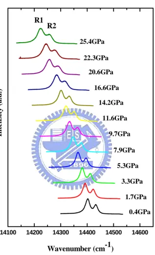
In order to generate a hydrostatic pressure environment for samples, a fluid pressure medium is required. Various fluids have been used, but a 4 : 1 methanol-ethanol mixture has been proved to be very popular. Unfortunately, the use of fluids is valid only to about 10 GPa, since most liquids become solids above this pressure. Deionized -water is also considered to be a pressure medium, but it transfers to solid ice VI and ice VII at 0.6 and 2.1 GPa, respectively.
However, previous study shown that the R1-R2 splitting in the ruby fluorescence was maintained well up to 16.7 GPa, therefore, the non-hydrostatic components of water is not a serious problem below 16.7 GPa [15]. In the present study, such a splitting was well recorded up to 25.4 GPa as shown in Fig. 2.3. Hence, deionized -water seems to be a suitable pressure medium in the high pressure study. For the reason we choose deionized -water pressure medium in our experiments.
2.2-3 Pressure Calibration
Various methods of pressure calibration involving the DAC have been used. Pressure in the DAC was estimated by calculating force over area, the known fixed point, and in high-pressure X-ray studies by internal markers such as NaCl or silver. However, these methods are not convenient and are often proved to be inaccurate.
With the introduction of the ruby fluorescence method in 1972 by Foreman et al. [16] a major obstacle with the DAC, namely, pressure calibration, was removed,
clearing the way for widespread use of the DAC for high-pressure physical investigation. Foreman et al. first showed the R-line on Cr+3-doped Al2O3 shift linearly
with hydrostatic pressure in the range of 0.1-2.2 GPa, and that the R-line broadens if the ruby experiences non-hydrostatic stresses. A tiny ruby chip of 5-10 μm in the pressure medium along with the sample, and the fluorescence of the ruby chip is excited by either a Ar+2 laser line or any source of strong light. Fig. 2.4 shows the energy levels and the resulting absorption and luminescence for Cr+3 ions in ruby [17].
Piermarinal et al. [18] calibrated the R-line to 19.5 GPa against the compression of NaCl by using Decker equation of state for NaCl. The R-lines of ruby are intense, and the doublet R1 and R2 have the delta wavelength 964.2 and 692.7 nm, respectively, at atmospheric pressure. At high pressure these shifts to higher wavelength and the shift is measured linearly with increasing pressure.
2.3 Micro-Raman Scattering Experiments
2.3-1 The Principle of Raman Scattering
All the Raman parameters – band frequencies and intensity, line shape and linewidth, polarization behavior – can be used to characterize the lattice, impurities, and free carriers in a semiconductor. The intensity gives information about crystallinity. The linewidths increase when a material is damaged or disordered, because these conditions increase the phonon damping or break the momentum conservation during the Raman scattering process. The strengths and frequencies of the phonons can be used to determine the degree of alloying in a ternary material [19].
encounters the surface of a semiconductor, the following situations can usually occur: for example, reflected, transmitted, absorbed, or Rayleigh scattered. In these situations, there are no change in photon frequency. However, a small fraction of light may interacts elastically with phonon modes, producing outgoing photons whose frequencies are shifted from the incoming ones. These are the Raman-scattered photons. The interaction of the incident light with optical phonons is called Raman scattering. When the polarization of optical phonon is transverse (longitudinal) relative to their wavevector of photon, it is call TO (LO) mode. Photon gains energy by absorbing a phonon (anti-Stokes shifted), or loses energy by emitting one (Stokes shifted). The law of conservation energy and momentum must be applied in the process. The conservation conditions are
0 hv hv hvs = i ± , (2.1) 0 k k ks = i± , (2.2) Where the subscript “s” in the formula stands for scattering: “i ” stands for
incident and “0” stands for optical phonon. The puls sign stands fot anti-Stokes shift and minus sign is stands for Stokes shift. Normally, the intensity of the anti-Stokes modes is much weaker than that of the Stokes components, because usually these are few phonons to be absorbed compared to the density of phonons that can be emitted. Raman scattering is inherently a weak process, but lasers provide enough power such that the spectra can be routinely measured [20].
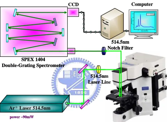
2.3-2 Experimental Setup
The schematic diagram of the Raman scattering experiment is shown in Fig. 2.5. In this work, the Raman scattering measurements were performed by a Jobin-Yvon micro-Raman system. The Raman spectra at room temperature were excited by using
the 514.5 nm line from an argon-ion laser. Usually, a laser beam with a power of 90 mW was focused to a size of about 2 μm on the sample surface in the DAC. To exclude the Reyleigh scattering, we used notch filter to filter out the Reyleigh scattering of the laser. The intensity of Raman lines were normalized to the power of the laser as measure by a power meter and the backscattering Raman signals were collected by the SPEX 1404 double-grating spectrometer and detected by a LN2 cooled charge coupled
device (CCD). The spectrometer was controlled by a computer, which was used to store and plot the collected data.
2.4 Experimental Process
The Zn1-xCdxSe epilayers grown by MBE were ground into thin films with the
thickness of 100 μm the followed by chemical etching using NaOH mixed with H2O2
and deionized-water to remove the GaAs substrate. To obtain high pressure up to about 20 GPa, the Zn1-xCdxSe epilayers and ruby chip (about 1 μm in size) were sealed with
the pressure transmitting medium (deionized-water) in the sample chamber which was a hole of 170 μm diameter and 100 μm thick drilled on gasket which has an original thickness of 250 μm. The epilayers without GaAs substrates were loaded along with ruby powder into a diamond anvil cell. The pressure determination was done by reading the peak position of the ruby R1 fluorescence line.
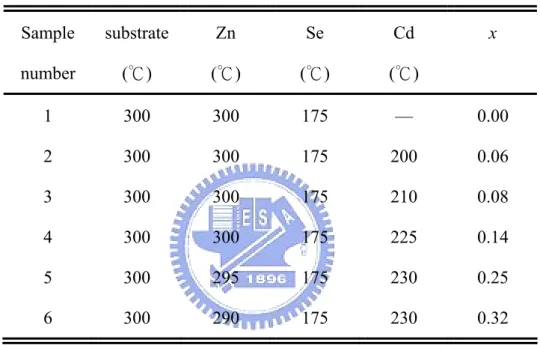
Table 2-1 Growth condition of Zn1-xCdxSe epilayers. Sample substrate Zn Se Cd x number ( )℃ ( )℃ ( )℃ ( )℃ 1 300 300 175 — 0.00 2 300 300 175 200 0.06 3 300 300 175 210 0.08 4 300 300 175 225 0.14 5 300 295 175 230 0.25 6 300 290 175 230 0.32
1-x x
μ
14100 14200 14300 14400 14500 14600 R2 R1 25.4GPa 22.3GPa 9.7GPa 5.3GPa 11.6GPa 14.2GPa 16.6GPa 7.9GPa 3.3GPa 1.7GPa 0.4GPa 20.6GPa Inte ns it y (a.u. ) Wavenumber (cm-1)
Fig. 2.3 Ruby fluorescence verse pressure in a pressure medium of deionized-water. The right -hand and left -hand side peaks of the plots present R1
Fig. 2.4 Energy level of Cr+3 in Al2O3. The transitions of E1/2→A and E3/2→A
CCD Computer 200 400 600 0 5000 10000 15000 20000 In te ns it y ( a .u .) Raman shift (cm-1) ZnSe Ar+Laser 514.5nm 514.5nm Laser Line 514.5nm Notch Filter SPEX 1404 Double-Grating Spectrometer power ~90mW power ~90mW CCD Computer 200 400 600 0 5000 10000 15000 20000 In te ns it y ( a .u .) Raman shift (cm-1) ZnSe Ar+Laser 514.5nm 514.5nm Laser Line 514.5nm Notch Filter SPEX 1404 Double-Grating Spectrometer power ~90mW power ~90mW 200 400 600 0 5000 10000 15000 20000 In te ns it y ( a .u .) Raman shift (cm-1) ZnSe Ar+Laser 514.5nm 514.5nm Laser Line 514.5nm Notch Filter SPEX 1404 Double-Grating Spectrometer power ~90mW power ~90mW
Chapter 3
Result and Discussion
3.1 Raman Scattering of Zn
1-xCd
xSe Epilayers at
Atomspheric Pressure
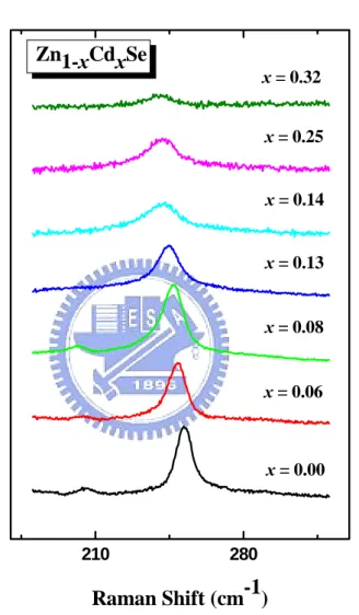
We have measured the phonon frequencies of the Zn1-xCdxSe epilayers at room
temperature and various pressures by Raman scattering system. In the backscattering geometry used in our experiment, the LO phonon mode is allowed while the TO phonon mode is forbidden. For the Raman scattering experiment, the GaAs substrate were removed by mechanical polishing. At atmospheric pressure, two peaks labeled as TO phonon mode and LO phonon mode are observed for each Zn1-xCdxSe epilayer in
Fig. 3.1. For x = 0.00, the TO and LO are observed at 205.3 cm-1 and 252.1 cm-1, respectively. For x = 0.06, the TO and LO are observed at 203.1 cm-1 and 248.5 cm-1, respectively. For x = 0.08, the TO and LO are observed at 201.4 cm-1 and 246.6 cm-1, respectively. We only observe one peak labeled as LO for x = 0.14, x = 0.25, and x =
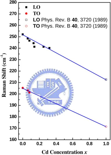
0.32 at atmospheric pressure. The LO are observed at 241.3 cm-1, 241.3 cm-1, and 240.2 cm-1, respectively. The variation of these phonon frequencies with Cd concentration fraction x is shown in Fig. 3.2. In this figure, phonon frequencies of
CdSe obtained from other reference are also shown by open circle and open square [21]. From this figure, Raman measurements on samples of MBE grown Zn1-xCdxSe
epilayers show a linear variation of frequencies with the Cd concentration fraction x.
The Raman peaks of Zn1-xCdxSe epilayers decrease frequency and increase linewidth
with the increasing Cd concentration. It implies the softening of the lattice. This agrees with the observation that the high Cd concentration increases alloy potential
fluctuation [1]. With increasing Cd concentration, the phonon vibration mode has a redshift, and the mode intensity weakens. The fact that the atomic radius of Cd is greater than Zn leads to the increase in lattice constant. As a result, the frequencies of the quasi-harmonic vibration of the crystal should be decreased. As shown in this figure, the results of our experiments reveal that Zn1-xCdxSe is a one-mode system.
Whether a mixed crystal system A1-xBxC will exhibit one-, two-, and mixed-mode
behavior type depends almost entirely on the relative masses of the atoms A, B, and C. In the one-mode behavior, the zone-center optical phonon frequencies vary continuously with concentration within the frequencies of the two end members. In two-mode behavior, each TO-LO phonon pair for an end members degenerates to an impurity mode of the other end member. Between these limits lies the mixed-mode, which shows intermediate behaviors. Based on this consideration, Chang and Mitra have derived a criterion in order to determine the one-, two-, or mixed-mode behavior type [22]. The criterion for one mode behavior is mA > μBC i.e. for one-mode mixed
crystal, the mass of one substituting element is smaller than the reduced mass of the compound formed by the other elements, at both ends of its composition range [23]. If this is violated the alloy will exhibit two-mode behavior. In our considerations, the masses of each component are chosen as follows: mZn = 65.38 amu., mCd = 112.41
amu., and mSe = 78.96 amu.. For Zn1-xCdxSe, the mass of Cd is greater than the
reduced mass of ZnSe, and the mass of Zn is greater than the reduced mass of CdSe. As a result, Zn1-xCdxSe epilayers exhibits one-mode behavior for all values of x
between 0 and 1. It is in agreement with our experimental results. However, there is some controversy in the literature. Alonso et al. performed Raman measurements on Zn1-xCdxSe in the whole compositional range [21]. They found Zn1-xCdxSe exhibites a
Zn1-xCdxSe [24]. However, more recent Raman measurements seem to support that
Zn1-xCdxSe has a one-mode behavior [23, 25, 26].
3.2 Raman Scattering of Zn
1-xCd
xSe Epilayers at
High Presssure
For the high-pressure Raman scattering experiments, high pressures were generated by using the diamond anvil cell. When the pressure is increased, the force acted on the crystal becomes larger and this force will compress the whole volume of the crystal. Therefore the distances among atoms would accordingly decrease. When atoms become closer to each other, the repulsion force induced by outer-shell electrons of neighboring atoms becomes larger and larger. And this makes the whole crystal unstable. As a result, the whole crystal structure would change to a more stable crystal structure. The structure change could induce energy shift of phonon, and it can be studied by Raman scattering. The Raman spectroscopy of Zn1-xCdxSe epilayers for x =
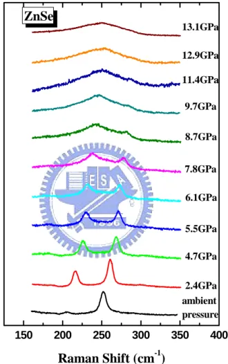
0.00, 0.06, 0.08, 0.14, 0.25, and 0.32 at various pressures and room temperature are shown in Fig. 3.3-3.8. In Fig. 3.3-3.8, intensities of all these Raman modes decrease as the pressure is increased. According to Fig. 3.3-3.8, we find that the LO phonon modes disappeared and the TO phonon modes broaden at different pressure. For x = 0.00, the
LO phonon mode disappeared and TO phonon mode broadened at 12.9 GPa. For x =
0.06, the LO phonon mode disappeared and TO phonon mode broadened at 12.3 GPa. For x = 0.08, the LO phonon mode disappeared and TO phonon mode broadened at
11.4 GPa. For x = 0.14, the LO phonon mode is disappeared and TO phonon mode
broadened at 7.1 GPa. For x = 0.25, the LO phonon mode disappeared and TO phonon
mode broadened at 10.0 GPa. For x = 0.32, the LO phonon mode disappeared and TO
pressure was identified by the energy-dispersive x-ray diffraction (EDXD) result which corresponds to a change of the crystal structure and accompanies the disappearance of the LO phonon mode [8]. As x is increased, the semiconductor to metal-transition
pressure decreased. However, we have found the transition pressure increased when Cd concentration x is increased from 0.14 to 0.25. The transition pressures of the
Zn1-xCdxSe epilayers for x up to 0.32 are plotted in Fig. 3.15. The decrease in transition
pressure with x implies the decreasing crystal stability with x. However, the reason of
the increase in transition pressure is unidentified.
The variation of Raman shift of LO and TO for ZnSe, Zn0.94Cd0.06Se,
Zn0.92Cd0.08Se, Zn0.86Cd0.14Se, Zn0.75Cd0.25Se, and Zn0.68Cd0.32Se epilayers as a function
of pressure are shown in Fig. 3.9-3.14, respectively. The circles and squares represents for TO mode and LO mode, respectively. The lines are quadratic polynomial fitting lines that conclude the behavior of each Raman modes with increasing pressure. From these figures, one can clearly see the variation of different Raman modes at different pressures.
It is clear that for Zn1-xCdxSe epilayers with x = 0.00, 0.06, 0.08, 0.14, 0.25, and
0.32, all Raman modes blue shift to higher frequencies when the pressure increases. The relationship of these Raman mode frequencies versus pressure of ZnSe, Zn0.94Cd0.06Se, Zn0.92Cd0.08Se, Zn0.86Cd0.14Se, Zn0.75Cd0.25Se, and Zn0.68Cd0.32Se
epilayers can be obtained by the quadratic polynomial fitting and are plotted as the solid curve, in Fig. 3.9-3.14, respectively. The solid symbols shown in the figures are the results of our experimental data. The quadratic polynomial fitting formulas for ZnSe are expressed as follows:
2 252.1 3.28 0.041 LO P P ω = + − (3.1) 2 090 . 0 66 . 4 3 . 205 P P TO = + − ω (3.2),
for Zn0.94Cd0.06Se are expressed as follows: 2 165 . 0 73 . 4 7 . 248 P P LO = + − ω (3.3) 2 071 . 0 88 . 4 3 . 203 P P TO = + − ω (3.4), for Zn0.92Cd0.08Se are expressed as follows:
2 246.2 3.50 0.008 LO P P ω = + − (3.5) 2 071 . 0 95 . 3 3 . 205 P P TO = + − ω (3.6), for Zn0.86Cd0.14Se is expressed as follows:
2 208 . 0 55 . 2 2 . 243 P P LO = + − ω (3.7), for Zn0.75Cd0.25Se is expressed as follows:
2 041 . 0 73 . 3 5 . 241 P P LO = + − ω (3.8), similarly, for Zn0.68Cd0.32Se, the fitting formulas can be expressed as follows:
2 162 . 0 92 . 4 2 . 239 P P LO = + − ω (3.9), where ω is the wavenumber in cm-1 and P is the pressure in GPa.
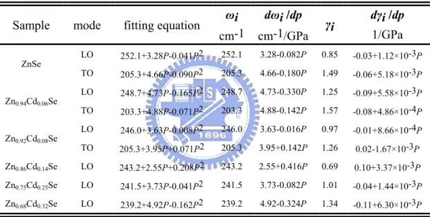
In general, the crystal ionicity can be expressed by the Grünesien parameters, which can be calculated from the pressure shifts of the LO and TO phonons of Zn1-xCdxSe measured by the micro-Raman scattering experiments. The Grünesien
parameter γi for a quasi-harmonic mode i of frequency ωi is defined by [27]
0 ln 1 ln ln i i i i i k d v p dp ω ω ω γ β ω ∂ ∂ = − = = ∂ ∂ (3.10), where β is the isothermal volume compressibility; v is the molar volume in cm3/mol; k is the bulk modulus for Zn0 1-xCdxSe. The bulk modulus of Zn1-xCdxSe is
unknown, but the values of k0ZnSe=65.6 GPa [28] and k0CdSe=54.6 GPa [29]. In our samples, Cd concentration x is low. Hence, k0Zn Cd Se1−x x was taken as 65.6 GPa from the
value of ZnSe at zero pressure. The pressure effect on Raman vibration modes of Zn1-xCdxSe at room temperature are shown in Table 3-1. As a comparison with
previous works [30], we found γTO >γLO for all Zn1-xCdxSe epilayers. This indicates
that as the crystal is compressed, there is a decrease in the ratio of LO and TO mode frequencies. Further, the calculated γTO /γLO for ZnSe, Zn0.94Cd0.06Se, and
Zn0.92Cd0.08Se are 1.752, 1.256, and 1.298, respectively. This manifests that ZnSe has a
higher ionicity than Zn0.94Cd0.06Se and Zn0.92Cd0.08Se.
We may use a spring model to explain why Raman modes blue shift to higher frequencies with increasing pressure. As mentioned before, the interaction force between any two neighboring atoms in a crystal can be considered as having a spring connecting to each other. The force constant of this spring will be different depending on the strength of chemical bonding between atoms. We may consider the force constants between atoms become larger as the pressure was increase. As a result, the phonon vibration energy increases as the pressure is increased.
Table 3-1 Effect of pressure on various Raman vibrational modes of Zn1-xCdxSe at
room temperature. The value of mode frequenciesωi, pressure dependenced i
dp ω
, and mode Grünesien parameter γi were obtained at ambient condition.
Sample mode fitting equation ωi cm-1 dωi /dp cm-1/GPa γi dγi /dp 1/GPa ZnSe LO TO 252.1+3.28P-0.041P2 205.3+4.66P-0.090P2 252.1 205.3 3.28-0.082P 4.66-0.180P 0.85 1.49 -0.03+1.12×10⁻³P -0.06+5.18×10⁻³P Zn0.94Cd0.06Se LO TO 248.7+4.73P-0.165P2 203.3+4.88P-0.071P2 248.7 203.3 4.73-0.330P 4.88-0.142P 1.25 1.57 -0.09+5.58×10⁻³P -0.08+4.86×10⁻⁴P Zn0.92Cd0.08Se LO TO 246.0+3.63P-0.008P2 205.3+3.95P+0.071P2 246.0 205.3 3.63-0.016P 3.95+0.142P 0.97 1.26 -0.01+8.66×10⁻⁴P 0.02-1.67×10⁻³P Zn0.86Cd0.14Se LO 243.2+2.55P+0.208P2 243.2 2.55+0.416P 0.69 0.10+3.37×10⁻³P Zn0.75Cd0.25Se LO 241.5+3.73P-0.041P2 241.5 3.73-0.082P 1.01 -0.04+1.44×10⁻³P Zn0.68Cd0.32Se LO 239.2+4.92P-0.162P2 239.2 4.92-0.324P 1.34 -0.11+6.30×10⁻³P
210 280 Zn1-xCdxSe Ram a n In te nsity (a.u .) Raman Shift (cm-1) x = 0.08 x = 0.00 x = 0.06 x = 0.14 x = 0.25 x = 0.32 x = 0.13
Fig. 3.1 Raman spectra of Zn1-xCdxSe for x = 0.00, 0.06, 0.08, 0.13, 0.14, 0.25,
0.0 0.2 0.4 0.6 0.8 1.0 160 170 180 190 200 210 220 230 240 250 260 270 280 R a man Shif t ( cm -1 ) Cd Concentration x LO TO LO Phys. Rev. B 40, 3720 (1989) TO Phys. Rev. B 40, 3720 (1989)
Fig. 3.2 Composition dependence of the zone-center optical phonon frequencies in zinc-blende Zn1-xCdxSe.
150 200 250 300 350 400 ZnSe 5.5GPa 8.7GPa 12.9GPa 13.1GPa 11.4GPa 9.7GPa 7.8GPa 6.1GPa 4.7GPa 2.4GPa ambient pressure Ram a n In te nsi ty (a.u.) Raman Shift (cm-1)
150 200 250 300 350 400 Zn0.94Cd0.06Se 11.4GPa 6.6GPa 4.8GPa 12.3GPa 11.9GPa 0.9GPa 8.9GPa 2.6GPa 7.5GPa ambient pressure R ama n Int ensity ( a. u .) Raman Shift (cm-1) x2
200 250 300 350 Zn0.92Cd0.08Se 11.4GPa 10.4GPa 9.4GPa 8.6GPa 7.5GPa 2.2GPa 3.4GPa 4.5GPa 6.1GPa ambient pressure x2 Raman Inte nsity (a.u.) Raman Shift (cm-1) x2
200 250 300 350 7.1GPa 6.9GPa 6.8GPa 6.7GPa 5.1GPa 4.3GPa 3.4GPa 2.0GPa 1.2GPa 0.2GPa ambient pressure Zn0.86Cd0.14Se R am an Inte nsity (a.u.) Raman Shift (cm-1)
200 250 300 350 Zn0.75Cd0.25Se 10.0GPa 9.7GPa 9.3GPa 8.5GPa 7.6GPa 6.6GPa 4.5GPa 3.1GPa 2.4GPa 0.6GPa ambient pressure R ama n Int ensity ( a. u .) Raman Shift (cm-1)
180 270 360 9.5GPa 9.2GPa 8.1GPa 7.5GPa 6.6GPa 5.6GPa 4.3GPa 3.6GPa 2.8GPa 1.8GPa ambient pressure Zn0.68Cd0.32Se R a ma n Int ensit y ( a .u .) Raman Shift (cm-1)
0 2 4 6 8 10 12 14 16 190 200 210 220 230 240 250 260 270 280 290 300 11.4GPa R a man Shif t ( c m -1 ) Pressure (GPa) TO LO
0 2 4 6 8 10 12 14 200 210 220 230 240 250 260 270 280 290 300 R a man Shif t ( c m -1 ) Pressure (GPa) TO LO 11.9GPa
0 2 4 6 8 10 12 190 200 210 220 230 240 250 260 270 280 290 300 Ra ma n Shif t ( c m -1 ) Pressure (GPa) TO LO 10.4GPa
0 2 4 6 8 10 190 200 210 220 230 240 250 260 270 280 290 300 6.9GPa LO R a ma n Shif t ( c m -1 ) Pressure (GPa)
0 2 4 6 8 10 190 200 210 220 230 240 250 260 270 280 290 300 9.7GPa R a man Shif t ( c m -1 ) Pressure (GPa) LO
0 2 4 6 8 10 190 200 210 220 230 240 250 260 270 280 290 300 9.2GPa R a man Shif t ( c m -1 ) Pressure (GPa) LO
0.0 0.1 0.2 0.3 0.4 6 7 8 9 10 11 12 13 14 15 Zn1-xCdxSe Pr essur e (GPa) Cd Concentration x
Fig. 3.15 Concentration dependence of transition pressure for Zn1-xCdxSe
Chapter 4
Conclusion
The pressure-induced structural phase transition of Zn1-xCdxSe epilayers was
investigated using the micro-Raman scattering experiment. From the Raman scattering experiment, we have measured the frequencies of LO and TO phonons in Zn1-xCdxSe epilayers for x = 0.00, 0.06, 0.08, 0.14, 0.25, and 0.32 at room temperature
and various pressures. Indirect observation of the metallization of semiconductors was proposed. The disappearance of the LO phonon is attributed to the metallization of the Zn1-xCdxSe epilayers. The pressure-induced metallization for ZnSe, Zn0.94Cd0.06Se,
Zn0.92Cd0.08Se, Zn0.86Cd0.14Se, Zn0.75Cd0.25Se, and Zn0.68Cd0.32Se epilayers occurred
at 12.9, 12.3, 11.4, 7.1, 10.0, and 9.5 GPa, respectively. The observed reduction in the structural transition pressure of Zn1-xCdxSe with Cd concentration implies that the
replacement of Zn by Cd results in a decrease in the metallization pressure. This also indicates that the replacement of Zn by Cd results in a softening of the crystal bonding and instability of the crystal structure. The pressure variation of the phonon frequencies and Grünesien parameters of the two optical modes were also calculated.
References
[1] W. Meredith, G. Horsburgh, G. D. Brownlie, K. A. Prior, B. C. Cavenett, W. Rothwell, and A. J. Dann, J. Cryst. Growth 159, 103 (1996).
[2] M. A. Haase, J. Qiu, J. M. Depuydt, and H. Cheng, Appl. Phys. Lett. 59, 1272 (1991).
[3] J. Ding, H. Jeon, T. Ishihara, M. Hagerott, and A. V. Nurmikko, H. Luo, N. Samarth, and J. Furdyna, Phys. Rev. Lett. 69, 1707 (1992).
[4] S. Ves, K. Strössner, N. E. Christensen, C. K. Kim, and M. Cardona, Solid State Commun. 56, 479 (1985).
[5] M. I. McMahon and R. J. Nelmes, J. Phys. Chem. Solids 56, 485 (1995). [6] R. G. Greene, H. Luo, and A. L. Ruoff, J. Phys. Chem. Solids 56, 521
(1995).
[7] G. Itkin, G. R. Hearne, E. Sterer, M. P. Pasternak, and W. Potzel, Phys. Rev. B 51, 3195 (1995).
[8] C. M. Lin, D. S. Chuu, T. J. Yang, W. C. Chou, J. A. Xu, and E. Huang, Phys. Rev. B 55, 13641 (1997).
[9] M. P. Halsall, P. Harmer, P. J. Parbrook, and S. J. Henley, Phys. Rev. B 69, 235207 (2004).
[10] C. Pinquier, F. Demangeot, J. Frandon, J. W. Pomeroy, M. Kuball, H. Hubel, N.W. A. van Uden, D. J. Dunstan, O. Briot, B. Maleyre, S. Ruffenach, and B. Gil, Phys. Rev. B 70, 113202 (2004).
[11] C. Pinquier, F. Demangeot, J. Frandon, J. C. Chervin, A. Polian, B. Couzinet, P. Munsch, O. Briot, S. Ruffenach, B. Gil, and B. Maleyre, Phys. Rev. B 73, 115211 (2006).
Phys. Chem. Solids 56, 563 (1995).
[13] A. K. Arora, and T. Sakuntala, Phys. Rev. B 52, 11052 (1995).
[14] A. K. Arora, E. K. Suh, U. Debska, and A. K. Ramdas, Phys. Rev. B 37, 2927 (1988).
[15] J. Xu, J. Yen, Y. Wang, and E. Huang, High Pressure Research 15, 127 (1996).
[16] R. A. Forman, G. J. Piermarini, J. D. Barnett, and S. Block, Science 176, 284 (1972).
[17] E. Huang, J. Geol. Soc. China 32, 924 (1992).
[18] G. J. Piermarini and S. Block, Rev. Sci. Instrum. 46, 973 (1975).
[19] A. Chergui, J. Valenta, and J. L. Loison, Semiconductor Science Technology 9, 2073 (1994).
[20] J. I. Packove, Optical Processes in Semiconductors, Dover, New York (1971).
[21] R. G. Alonso, E. K. Suh, A. K. Ramdas, N. Samarth, H. Luo, and J. K. Furdyna, Phys. Rev. B 40, 3720 (1989). I. F. Chang and S. S. Mitra, Phys. Rev. 172, 924 (1968).
[22] I. F. Chang and S. S. Mitra, Phys. Rev. 172, 924 (1968).
[23] W. Meredith, G. Horsburgh, G. D. Brownlie, K. A. Prior, B. C. Cavenett, W. Rothwell, and A. J. Dann, J. Crystal Growth 159, 103 (1996).
[24] J. Camacho, I. Loa, A. Cantarero, K. Syassen, I. Hernández-Calderón, and L. Gonzálz, Phys. Stat. Sol. (b) 235, 432 (2003).
[25] W. S. Li, Z. X. Shen, D. Z. Shen, and X. W. Fan, J. Appl. Phys. 84, 5198 (1998).
286 (1999).
[27] M. Cardona and G. Güntherodt, Light Scattering in Solids IV, Springer, Berlin (1984).
[28] O. Madelung, Semiconductors :Data Handbook, Springer, Berlin (2004). [29] F. Benkabou, H. Aourag, and M. Certier, Mater. Chem. Phys. 66, 10
(2000).
[30] S. S. Mitra, O. Brafman, W. B. Daniels, and R. K. Crawford, Phys. Rev.