A
Wide-stopband Low-pass Filter Design Based
on
Multi-period
Taper-etched EBG Structure
Yin-Chi Chen, An-Shyi Liu, and Ruey-Beei
Wu
Department
of Electrical Engineering and Graduate Institute of Communication Engineering National
Taiwan University Taipei, Taiwan 106, R.O.C.
Abstract - Electromagnetic bandgap (EBG) microstrip
structures have been proposed in theapplication ofantennaand microwave filter design. The paper demonstrates a design procedurefor the EBG structure to achieve a wide stopband low-pass filter, by combining tapered etched holes and multi-period EBG structure. The measurement result shows the rejection band is from 5.2 GHz to 25 GHz, which meets the simulation result.
Index Terms Electromagnetic bandgap, multi-period EBG
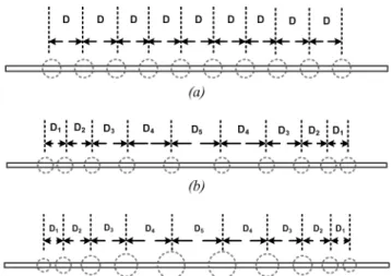
D D 'D ' D ' D ' D 'D D D
D:DD :D : Di:
(a)
:01 :02 :03: 0D4 : 5: 0D4 : 2:02 1
I. INTRODUCTION
(b)
A periodic structure which may exhibit the rejection of a certain frequency band is called photonic bandgap (PBG) or
electromagnetic bandgap (EBG)structure. The applications of EBG structure in microstrip technology investigated in literatures are concentrated on antenna and microwave filter design [1]-[7]. The main mechanism of EBG integrated
antennaisto suppress surfacewavewhile the EBG integrated filteris to rejecta frequencyband. The aim of this work is to
designanEBGstructure as awidestopband low-pass filter.
In conventional microwave filter design, the undesired
frequency suppression has been usually implemented using
shorted-circuited stub or surface-mounted capacitor. The shorted-circuited stub is one-halfguided wavelength long at
the frequency to be rejected and occupies some circuit area.
Onthe other hand, the surface-mounted capacitoris suitable for low-frequency applications and its parasitic effect becomes severe as the frequency increases. It is difficult to
estimate theparasitic effect owing to fabrication discrepancy
in the design procedure. Therefore, another resolution which is a simple pattern ofperiodic holes or structures etched in
ground plane beneath the strip conductor, has beenproposed
forlow-pass filter design[2]-[7].
Two-dimensional (2-D) periodic patterns etched in ground plane formicrostrip lines were first proposed [2]-[3]. Owing
to the highly confined field around the strip conductor, the
structure is then reduced to one-dimensional (1-D) ones in
some literature [4]-[7]. Although atheoretic studyto analyze
therejection frequencyband of 1-DEBGmicrostripstructure
has been proposed [4], it considers only the design that the ratio of radius of etched circular holestoseparationbetween
This work was supported in partby the National Science Council, Taiwan, ROC,under Grant NSC 93-2752- E-002-003-PAE.
D1:2: D3: D D3 D2 D1
Fig. 1 Schematic representations of differentEBGstructures.
(a) single-period, (b) multi-period, and (c) multi-period with
tapered etched holes.
centers ofadjacent holes are kept the same. Such a design does not provide optimal bandwidth ofrejection band for a
given number of etched holes. Other designs for wider rejection bandcanbeimplemented, suchasby cascaded EBG
microstrip circuit [3], taper structure in ground plane [6], or
multi-period EBGstructure
[6]-[7].
The structure proposed in this paper is based on a combination of tapered etched holes and multi-period EBG structure. With suitable choice of the radius ratio and the
separation of adjacent holes, a novel wide rejection band, which is from 5.2 GHzto 25 GHz, canbe obtained. The first section describes how the EBG structure was designed. It is followedby asectiondescribingthe simulation and measured
results,and then is the conclusion.
II.DESIGNANDANALYSISOFEBG STRUCTURES
SeveraltypicalEBGstructureswith etched circular holes in
ground plane ofa50Q microstriplineare shown inFig. 1. In the design procedure, single-period structures shown inFig. l(a) were first analyzed by Ansoft Ensemble 8.0 [8] with
separations D as a parameter. The central frequency, depth, and bandwidth of the forbidden band for the 1-D EBG structure can be determined by the separation of adjacent
holes in the ground plane (D), the hole radius (R), and the number of holes
(N)
[4].For a single-period EBG structure, the central frequency of the first stopband can be roughly determined by the periodD
using the formula [1]:
c 1
f
=~-e
- (1)where c is thespeedoflightinfree space, and
Ag
=2 Dis theBragg condition. Recently, a more accurate expression for the Bragg condition has been proposed [5], which takes into account the change in the effective dielectric constant of the microstrip line
eff
produced by the pattern etched in the ground plane. For a microstrip line with etched ground plane, the effective dielectric constant6eff
canbe estimated as that of the line withunperturbed ground plane, i.e.,8rC+1 cr 1 1
8eff
2 + 2 + (2)where d and W are the thickness of the substrate and the width of theline, respectively.
The structure considered here has parameters -r= 3.38 (Rogers R04003), d=20mils, and W=1.2 mm, corresponding
to a50Q conventional microstripline. Tobegin with, the unit lattice is chosen to be a circle with uniform radius for investigating the bandgap characteristics. The bandwidth of
bandgap can be estimated by full-wave analysis with the
separation of aduacent holes, D, as a parameter. In order to
achieveatnon-overlapping band gap,one canthen determine
a setofseparationsbetween adjacent circles,
Di's.
The radius of etchedcircles, R, is chosen between the line width andonehalf-wavelength. A small circle degrades the structure into a conventional microstrip and the band gap vanishes. A large
one acts as aslot patchwhen the radius reaches to one
half-wavelengthand increases radiation lossathigh frequency.
The second step is to determine the taper ratio ofadjacent
circles. For convenience, the ratio
Ri+IlRi
is set to be a constant so as to confine the radii of etched circles within the constraint mentioned in the above paragraph. Witha suitable selection of the taperratio, awide-band rejection bandcanbe obtained.III.SIMULATIONANDMEASUREMENT
In orderto investigate the stopbandbehavior of theproposed
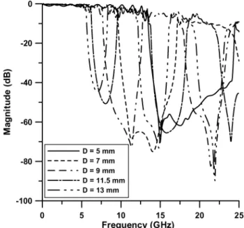
EBG structure, five single-period structures are analyzed, as
shown inFig. l(a). TheperiodD=5mm, 7mm, 9mm, 11.5mm, and 13mm is a parameter, while the etched holes radius is fixed at R=2mm.Simulation results of transmission (S21)are
shown inFig.2. The central frequencies of the first stopband
are 18.5GHz, 13.2GHz, 10.3GHz,
8.1GHz,
and 7.1GHz respectively, which shows that the central frequency of thestopbandobtainedby using (1)isagoodestimation.
Also noticed in Fig.2 is the non-overlapping stopband. This indicates that a linear combination of these periods may
contribute to a wider stopband response. In addition, the ratio RID's are 0.4, 0.29, 0.22, 0.17, and 0.15 respectively. As shown in Fig.2, a larger RID results in a wider stopband bandwidth. It is in good agreement with the result shown in
[1].
0 -20 m 0az .) -40 -60 -80 -100 0 5 10 15 20 25 Frequency(GHz)Fig. 2SimulatedS21parameter of single period 1-D EBG microstrip
structure.
TABLE I
DIMENSIONSFOR MULTIPERIOD
EBG STRUCTURE i
Di
(MM) R (mm)RIo
/Ri 1 5 2 2 7 2 3 9 21.O
4 1t5 21tO
5 13 2The five single-period EBG structures are cascaded in seriesto forma 1-Dmulti-periodEBGstructure, as shown in
Fig.l(b). Table I lists the separations
Di
ofadjacent circles. The simulated S parameters are shown in Fig.3. It is foundthat the stopband of this multi-period EBG structure is
widenedowingto thecascading of the individual stopbands..
The stopbandobtained for themulti-period EBGisjustlike a
combination of the stopbandsof the fivesingle-periodEBG. The presence of apassband around 10 GHz in Fig.3 depicts
that the design is not good enough. A better approach for
performance upgrade is to adopt a tapered EBG microstrip
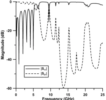
device [4], with the parameters listed in Table II. The simulated results in Fig.4 show that the passband around 10 GHz is successfully suppressed, and an impressive wide
stopband and high rejection level can be observed. Good agreement is also found between the measurements and the full-wave simulated data.
0 -20 5 15 IS21 -60-0 5 10 15 20 Frequency(GHz)
Fig. 3 Simulated S21 parameter of multi-period microstripstructure. m
'a
.) 1-D -_ - 1S111(Ensemble)\4 - -- IS21 (Ensem ble)
. --- - IS111(Measurement)
IS211(Measurement) ;;
TABLE II
OPTIMAL DIMENSIONSFOR
MULTIPERIOD EBG STRUCTURE
I Dii(mm)
RI
(mm)}R
1+i/R
1 5 1.67 12 2 7 24001.2
3 9 24012
4 11.5 2.88 1.2 5 13 3.46 2 IV. CONCLUSIONThe behavior of EBG structures with etched circles in ground plane is studied. It is shown that their associated stopbands can be joined together to form a very wide stopband by cascading different periods. The multi-period
EBG structure constructed according to this principle still remains in 1-D, which is of immediate interest for the design
offilters.
25 It is also demonstrated that a wide stopband low pass
filter
can be achieved by employing the tapered etched circles in EBG ground plane. This novel device can be used to perform broadband filtering of undesired frequencies, overcoming the narrowbandtechniques commonlyusedtoday. Otherpossible applications, such asfilters, frequency-selective surfaces, and efficient antenna structures,requirefurther studies.
.I
'I
0 10 20
Frequency (GHz)
Fig. 4 Simulated and measured S21 parameter of optimal multi-period1-DEBGmicrostripstructure.
REFERENCES
[1] R. Coccioli, F. R. Yang, K. P. Ma, and T. Itoh, "Aperture-coupled patch antenna on UC-PBG substrate," IEEE Trans. MicrowaveTheory Tech.,vol. 47, pp. 2123- 2130, Nov. 1999. [2] V. Radisic, Y. Qian, R. Coccioli, and T. Itoh, "Novel 2-D
photonic bandgap structure for microstrip lines", IEEE MicrowaveGuided. Wave Lett., vol. 8, pp. 69-71, Feb. 1998. [3] I. Rumsey, M. Piket-May, and P.K Kelly, "Photonic bandgap
structures used as filters in microstrip circuits", IEEE MicrowaveGuided Wave Lett., vol. 8, pp. 336-338, Oct. 1998. [4] M.A.G. Laso, M.J. Erro, D. Benito, M.J. Garde, T. Lopetegi, F.
Falcone, and M. Sorolla, "Analysisanddesignof1-D photonic bandgap microstrip structures using a fiber grating model", MicrowaveOptTechnol Lett., vol. 22, pp. 223-226, Aug.,1999. [5] M.A.G. Laso, T.Lopetegi, M.J.Erro, D. Benito, M.J. Garde,and
M, Sorolla, "Novel wideband photonic bandgap microstrip structures", MicrowaveOpt. Technol. Lett.,vol. 5,pp.357-360, 2000.
[6] M. A. G.Laso, T. Lopetegi, M. J. Erro, D. Benito, M. J. Garde, and M. Sorolla, "Multiple-frequency-tuned photonic bandgap microstrip structures,"IEEEMicroave Guided Wave Lett., vol. 10,pp.220-222,Jun.2000.
[7]C.C.Chiau,X. Chen and C.Parin,"MultiperiodEBGstructurefor wide stopband circuits", IEE Proc.Microwave Antennas Propag., pp. 489-492,Vol.150,Dec.2003.
[8]AnsoftEnsemble,softwarepackage developed byAnsoft Co.
4 1 I I I I I I I I I I I I I I I t ..Ii