方 得 華 博士
Te-Hua Fang, Ph. D
國立虎尾科技大學 機電所/光電所 奈米科技實驗室
National Formosa University
奈米加工與奈米壓痕術之應用研究
Outline
zIntroduction
zThermal probe lithography
zMechanical lithography
zElectrochemical lithography
zNanoindentation
zNanodevices and characterization
zMolecular dynamics simulations
zConclusion
-3-Introduction
¾
¾
Length scale :
Length scale :
0.1-100
nm
nm
¾
¾
Metrology :
Metrology :
SEM, TEM,
SPM
SPM
(STM, AFM,
(STM, AFM,
FFM,SNOM, MFM,
FFM,SNOM, MFM,
…
…
)
)
¾
¾
Applications:
Applications:
Nanomaterial
Nanomaterial
Nanobiology
Nanoelectric and Optic
Nanoelectric and Optic
Nanotribology and
Mechanics
Nanotechnology
Nanotechnology
Basics of Nanotechnology
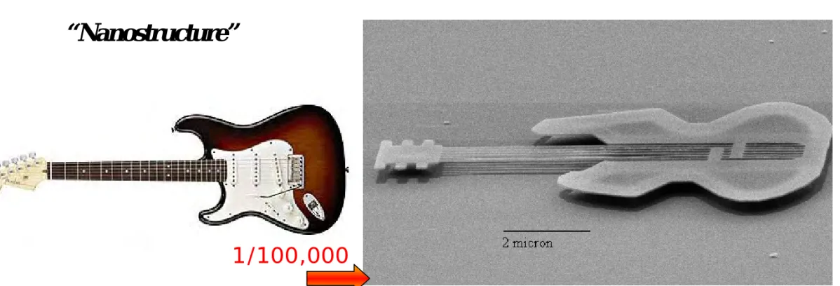
• Electron-microscope image of the world's smallest guitar, based roughly on the design for the Fender Stratocaster, a popular electric guitar.
• Its length is 10 millionths of a meter-- approximately the size of a red blood cell and about 1/20th the width of a single human hair. Its strings have a width of about 50 billionths of a meter (the size of approximately 100 atoms).
• Plucking the tiny strings would produce a high-pitched sound at the inaudible frequency of approximately 10 megahertz.
• Made by Cornell researchers with a single silicon crystal, this tiny guitar is a playful example of
nanotechnology, in which scientists are building machines and structures on the scale of billionths of a meter to perform useful technological functions and study processes at the submicroscopic level.
Figure cited from http://www.news.cornell.edu/science/July97/guitar.ltb.html, Dustin W. Carr and Harold G. Craighead, Cornell.
“Nanostructure”
Introduction
Nanostructured Materials
Carbon Nanotube
Au Nanoparticles
Teeth
X -Y ZNanoporous Alumina
Membrane
Sliding
Self-Assembling Monolayer
GaN nanotube
Butterfly wings
AFM Apparatus
Atomic manipulation
Xe/Ni (111)
Outline
zIntroduction
zThermal probe lithography
zMechanical lithography
zElectrochemical lithography
zNanoindentation
zNanodevices and characterization
zMolecular dynamics simulations
zConclusion
Thermal probe lithography
The rate of heat flow from the tip to the sample surface Q can be expressed as
Thermal probe lithography
Contact mode
Outline
zIntroduction
zThermal probe lithography
zMechanical lithography
zElectrochemical lithography
zNanoindentation
zNanodevices and characterization
zMolecular dynamics simulations
zConclusion
Mechanical Lithography
Mechanical Lithography
•The groove depth increased as the applied load increased and the groove depth for Au was larger than that of Pt under the same load.
•The volume of the removed material can be used to evaluate the hardness of the materials.
•On inspection of the volume removed at different loads, the volume was about
10,000 nm3 at a load of 1uN for Au and was approximately equal to that of a load of 2 uN for Pt. This result showed that the scratching hardness of the Pt film is higher than that of Au film.
Mechanical Lithography
•The wear depth of Au and Pt films measured as a function of feed at an applied force of 2.5uN and a speed of 2 um/s.
•When the nanomachining lateral feed was increased, the wear depth for both films decreased. The decreasing ratio of wear depth gradually became smaller as the feed rate was increased.
Mechanical Lithography
Computer aided nanomachining could be for the development of the next generation of
computer numerical control
(CNC) nano-scale machine tools
Outline
zIntroduction
zThermal probe lithography
zMechanical lithography
zElectrochemical lithography
zNanoindentation
zNanodevices and characterization
zMolecular dynamics simulations
zConclusion
Electrochemical lithography
1.Applied voltage 5.Pulse voltage 6.Electrical fields 2.Humidity 3.Hold time 4.Ionic diffusion 7.Surface roughness Tip : 2H2O+2e-Æ2H+ +2OH-Substrate, for example:SiSi+2OH-ÆSi2O+2H+
(a)
Water bridge
(b)Water bridge picture from Kelvin model
Molecular Simulation
30
(
) (
)
2 0 2 0 2 0r
-r
+
z
−
z
=
z
(
)
2
(
)
0
2
⋅
−
0+
⋅
−
0⋅
=
zr
dz
z
z
r
r
(
) (
)
2 0 2 0R
z
z
R
D
r
02+
+
−
=
+
0 0z
-R
D
r
tan
+
=
α
α
cos
⋅
−
+
=
D
R
R
h
α
sin
⋅
= R
r
1Electrochemical lithography
Electrochemical lithography
Effect of applied voltage
RH= 60% , Time of 5s
Time of 10s
Water bridge :(a) Higher Relative humidity (RH) (b) Lower RH
7
Effect of Humidity
Electrochemical lithography
GaAs, Voltage of 9V Relative humidity (RH) of 70% Time: 1, 2, 5 and 10s GaAs, Voltage of 9V RH of 50% Time: 1, 2, 5 and 10sApplied voltage of 10 V RH of 60% Time of 0.5, 1, 2,5 and 10s
⎟
⎠
⎞
⎜
⎝
⎛
⋅
=
h
h
u
exp
1
dt
dh
Effect of reaction time
GaAs, 10V, 70% and 10s GaAs, 10V, 70% and 150s
Ionic diffusion
Aspect ratio (h/W) of nanodots at different voltages
Contribution of nanodots at relative humidity
Ionic diffusion mechanism
Effect of pulse voltage
GaAs,RH of 65%, Time of 20s
Electrical field and growth rate
L LE
V
h
=
Electrochemical lithography
Effect of surface roughness
Applied voltage of 10V, RH of 60% and Time of10s
Effect of writing rate on producing nanowires
GaAs: 10, 9, 8 and 7 V
RH:60% ; Writing rate:60nm/s
Growth characteristics of different nanostructures
(a) GaAs
(b) Si
(c) TiN
Activation energies of SiO2, TiONxGa2O3and As2O3are 5eV, 1eV, 2eV and 3.6 eV, respectively
2GaAs + 12h++ 6H2O → Ga2O3 + As2O3+12H+ Si+2OH-ÆSiO2+2H + 2TiN+2O2Æ2TiO2+N2
Electrochemical lithography
Lithography with CNT probe
Outline
zIntroduction
zThermal probe lithography
zMechanical lithography
zElectrochemical lithography
zNanoindentation
zNanodevices and characterization
zMolecular dynamics simulations
zConclusion
Introduction to Nanoindentation
• Materials and Optoelectronic engineering :
Optimizing material
composition, structure, processing for particular applications (bulk and thin films)
•
Mechanics of small volumes:
Understanding whether thin films, lines, dots
have different mechanical properties than bulk counterparts
•
Material physics:
Measuring deformation processes such as dislocation
nucleation, crack growth, etc.
•
Indentation tests are the most commonly applied
means of testing the nanomechanical properties of
materials. The area of the residual indentation in the
sample is measured and the hardness, H, is defined
as H = P/A
r•
Nanoindentation refers to depth-sensing
indentation testing in the nanometer range and has
been made possible by the development of machines
and analysis models
•
Indentation tests are the most commonly applied
means of testing the nanomechanical properties of
materials. The area of the residual indentation in the
sample is measured and the
hardness
, H, is defined
as H = P/A
r•
Nanoindentation refers to depth-sensing
indentation testing in the nanometer range and has
been made possible by the
development of machines
Nanoindentation
Unique mechanics of small volumes in Materials
and Optoelectronic engineering
•Are mechanical properties affected by constraint?
•Are E, s
y, n f(size)?
•When structure dimensions approach atomic dimensions, is
mechanical behavior quantized?
•Are mechanical properties affected by constraint?
•Are E, s
y, n f(size)?
•When structure dimensions approach atomic dimensions, is
mechanical behavior quantized?
Elastic Contact Analysis
(
ν
)
π
A
E
S
21
2
−
=
s s i i rE
E
E
)
1
(
)
1
(
1
=
−
ν
2+
−
ν
2C
dP/dh
W
pW
eShow variables in response:
C = loading curvature
dP/dh = unloading stiffness
P
max, h
maxW
p= plastic work of indentation
W
t= total work of indentation
Experimental nanoindentation results
•The relative amount of pile-up is significantly smaller because a greater portion of the deformed volume is in the sample.
InGaN
XRD spectra (left) and AFM images (right) of InGaN films deposited at growth
temperatures of 790, 760 and 730 0C for In-content of (a)
InGaN
XRD spectra (left) and AFM images (right) of InGaN films deposited at growth
temperatures of 790, 760 and 730 0C for In-content of (a)
Nanoindentation of nanostructures
• Buckling characterization of vertical ZnO
nanowires using nanoindentation
Glass substrate 2 μm diameter circular flat diamond punch 300 350 400 450 500 550 600 3.26 eV (380 nm) PL Intensity (a.u.) Sample A Sample B Wavelength (nm) 20 30 40 50 60 70 80 ZnO (004) ZnO (002) Incident Angle (2θ) XRD Intensity (a.u) Sample B Sample A
200 400 600 800 1000 0 1k 2k 3k 4k 5k Unloading Loading
Sample A
Load
(
μN
)
Displacement (nm)
Pcr ~ 1465 μN 100 200 300 400 500 0 1k 2k 3k 4k 5k Pcr ~ 215 μNSample B
Load
(
μN
)
Displacement (nm)
Sample description σcr(MPa) K εcr(%) E (GPa) 0.5 0.62 117 0.7 0.32 229 0.5 0.35 232 0.7 0.18 454 B length: 800 nm diameter: 30 nm 806 A length: 2000 nm diameter: 100 nm 723
• Buckling characterization of vertical ZnO
nanowires using nanoindentation
Buckling
Outline
zIntroduction
zThermal probe lithography
zMechanical lithography
zElectrochemical lithography
zNanoindentation
zNanodevices and characterization
zMolecular dynamics simulations
zConclusion
Electrochemical lithography
combined with wet etching
(a)
(c)
(d)
BOE( Buffered Oxide Etch)-HF, NH4F and H2O
Application for Nanodevices
Electrochemical lithography
combined with wet etching
Current-voltages of nanodots
(a) I-V curve
(b) Fowler-Nordheim curve (ln(I/V
2) vs 1/V)
Fowler-Nordheim (FN)
Current density J:
⎟
⎠
⎞
⎜
⎝
⎛ −
=
E
E
C
J
0 2exp
β
C
0q
/
8
π
h
φ
B 3=
hq
m
*e B/
3
2
8
π
φ
3/2β
=
Current-voltages of nanodots
Nanoindentation of nanowires and
nanodots
Outline
zIntroduction
zThermal probe lithography
zMechanical lithography
zElectrochemical lithography
zNanoindentation
zNanodevices and characterization
zMolecular dynamics simulation
Molecular dynamics (MD)
• Simulation that shows how the atoms in the
system move with time
• Model phenomena that cannot be observed
experimentally
• Typically on the nanosecond timescale
• Solve the Newtonian equations of motion
Cons:
computationally demanding; no quantum description; no excited states;limited run time
Pros:
details model can describes certain aspects of nanoengineering very well;Nanomechanics
-a subset of the field of
nanotechnology, also sometimes called “Molecular
Mechanics” or “ Atomistic Simulation”
Quantum Mechanics Nano Mechanics Continuum Mechanics Microstructure Mechanics
nm
μm
mm
psec
nsec
msec
sec
Length
Time
fsec
Interaction
distance (nm)
interaction force (nN) (electromagnetic in origin)Get initial configuration
From crystallography or physical model
Assign initial velocities
At thermal equilibrium, the expected value of the kinetic
energy of the system at temperature T is:
This can be obtained by assigning the velocity
components v
ifrom a random Gaussian distribution with
mean 0 and standard deviation (k
B
T/m
i
):
How do we run a MD simulation?
T
k
N
v
m
E
B
N
i
i
i
kin
(
3
)
2
1
2
1
3
1
2
=
=
∑
=
For each time step:
Compute the force on each atom:
U is potential energy function
Solve Newton’s 2
ndlaw of motion for each atoms, to get new
coordinates and velocities
Store coordinates
Stop
X
U
X
U
X
F
∂
∂
−
=
−∇
=
(
)
)
(
)
( X
F
X
M
=
• •X: Cartesian vector of the system
M diagonal mass matrix
..
means second order
differentiation with
respect to time
How do we run a MD simulation?
Empirical Force Fields :
How do we run a MD simulation?
(
)
(
)
( )
[
]
∑
∑
∑
∑
∑
+
⎥
⎥
⎦
⎤
⎢
⎢
⎣
⎡
⎟
⎟
⎠
⎞
⎜
⎜
⎝
⎛
−
⎟
⎟
⎠
⎞
⎜
⎜
⎝
⎛
+
−
+
−
+
−
=
nonbonded j i ij j i nonbonded j i ij ij ij ij ij torsions all angles all bonds all br
q
q
r
R
r
R
n
K
K
b
b
K
U
, 0 , 6 12 2 0 2 04
2
cos
1
2
1
2
1
ε
πε
ε
φ
θ
θ
φ θ Torsion are 4-body Angles are 3-body Bonds are 2-body Non-bonded pairwise Angles Bonds TorsionU
bondsU
nonbondsHow do we run a MD simulation?
Many-body potential of the tight-binding second-moment approximation
(
TB-SMA
) model for Metals-Metals
)]
1
(
2
exp[
]
[
)]
1
(
exp[
0 2 1 2 1 0 0 0−
−
+
−
−
−
=
− −r
r
q
r
q
r
r
p
r
Ap
F
ij ijξ
φ
iφ
j ij∑
≠⎥
⎦
⎤
⎢
⎣
⎡
⎟⎟
⎠
⎞
⎜⎜
⎝
⎛
−
−
=
i j ij ir
r
q
1
2
exp
0φ
)}}
(
exp{
2
)}
(
2
{exp{
)
(
r
D
r
r
0r
r
0U
ij=
−
α
ij−
−
−
α
ij−
Morse
potential function for Metals-Diamond
Simulated nanoscratch
Process- constant depth
Simulated nanoscratch
Different tip shapes
Simulated nanoscratch
40x40x15a
Simulated nanoscratch
•The relationship of the wear depth and the temperature at an applied force of Fz = 570×10−10 N and Fy = 200×10−10 N and a simulated velocity of 250 m/s after being scratched is shown in above Figure.
• The wear depth increased while increasing the simulated temperature under the constant force due to increasing the kinetic
energy.
Simulated nanoscratch
•Figure illustrates the relationship of the wear depth and the velocity at an applied force of Fz = 570×10−10 N and Fy = 200×10−10 N and a temperature of 300K after being nanoscratched.
•The wear depth decreased while increasing the nanoscratching velocity. This is because the dislocations propagation in the material is difficult to make slip when the velocity was too fast and the diffusion time of the dislocations became shorter.
Molecular dynamics of nanoindentation
Molecular dynamics of nanoindentation
constant depth mode
Berkovich Recovery ratio~28.6% 209 adhesion atoms Vickers Recovery ratio~14.3% 74 adhesion atoms Sphere Recovery ratio~28% 418 adhesion atoms Cone Recovery ratio~14% 289 adhesion atoms
Molecular dynamics of nanoindentation
Simulated nanoindentation
•The plastic indentation depth, hp, is the depth of the permanent impression in the specimen after the removal of applied force and the plastic energy represents the area between the loading and unloading curves
• The plastic energy, Ur, depends on the indenter’s geometry, the operating
conditions, the material’s hardness, and the maximum of applied load, Pmax. The plastic energy is proportional to a function of the maximum applied load
•Load–displacement data for GaAs obtained during nanoindentation with a Berkovich
indenter showing pop-in behavior during loading
•The cross sectional view of the (0 1 0) plane corresponds to II–V steps
•3D MD simulation views of the dissociated dislocation loops,
•the cross-sectional view of dislocation loops surrounded the indenter tip and rotating 308 along the [1 1 1] plane (corresponding to the IV step), and
• top view of the MD simulation surface
showing the dislocation loops formed on and under the {1 1 1} plane. Red, green and blue represent the C, Ga and As atoms, respectively.
Outline
zIntroduction
zThermal probe lithography
zMechanical lithography
zElectrochemical lithography
zNanoindentation
zNanodevices and characterization
zMolecular dynamics simulations
Conclusion
•
Nanomachining Characterization
To achieve nanoscale fabrication
•
Mechanical and Thermal Lithography
•
Nanoelectrochemical Lithography
Acknowledgments
Thank NSC plans, STUT, NCKU, my students and coworkers~ L.W
Ji., S. L. Tasi, Y.H. Lin, S. R. Jian, J.D. Wu, W.I. Weng and W. J.
Chang etc
Literature
• T. H. Fang, C I Weng, J G Chang, Machining characterization of nano-lithography process by using
atomic force microscopy, NanotechnologyVol. 11. pp. 181-187, 2000.
• T. H. Fang, C I Weng, J G Chang, C C Hwang, Nanotribology of amorphous hydrogenated carbon
films by using a scanning probe microscopy,Thin Solid Films, Vol. 396, pp.166-172, 2001.
• T. H. Fang, C. I Weng, M. J. Chiang, Effect of substrate bias on nanotribology of a-C:H films
deposited by ECR-MPCVD,Diamond and Related Materials ,Vol. 11, pp.1653-1659, 2002.
• T. H. Fang, W. J. Chang, Effects of AFM-based nanomachining process on aluminum surface,
Journal of Physics and Chemistry of Solids, Vol. 64, pp.914-918, 2003.
• T. H. Fang, W. J. Chang, Microthermal machining using scanning thermal microscopy, Applied
Surface Science, Vol. 240, pp. 312-317, 2005.
• T. H. Fang, S. R. Jian, D. S. Chuu, Nanotribology and fractal analysis of ZnO thin films by using
scanning probe microscopy, Journal of Physics D: Applied Physics, Vol.36, pp.878-883, 2003.
• T. H. Fang, W. J. Chang, Nanoindentation characteristics on polycarbonate polymer film,
Microelectronics Journal, Vol. 35, pp. 595-599,2004.
• T. H. Fang, Mechanisms of nanooxidation of Si(100) from atomic force microscopy,
Microelectronics Journal, Vol. 35/9, pp 701-707, 2004.
• T. H. Fang, W. J. Chang, Nanolithography and nanoindentation of tantalum-oxide nanowires and
nanodots using scanning probe microscopy,Physica B: Condensed Matter, Vol. 352, pp. 190-199, 2004.
• T. H. Fang, W. J. Chang, C. M. Lin, Nanoindentation and nanoscratch characteristics of Si and GaAs,
Microelectronic Engineering, Vol. 77, 389-398, 2005.
• T. H. Fang , Oxidation characteristics of nanodot and nanobump on TiN thin films by atomic force
microscopy,Electrochimica ActaVol. 50/14 pp 2793-2797,2005.
• T. H. Fang, W. J. Chang, C. I. Weng, Surface analysis of nanomachined surface using atomic force
microscopy,Materials Chemistry and Physics, Vol.32, pp. 141-146, 2005.
• T. H. Fang, W. J. Chang, C. I. Weng, Nanoindentation and nanomachining characteristics of gold
and platinum thin films, Materials Science & Engineering A, Vol. 430, pp.332-340, 2006.
• T. H. Fang, K. T. Wu, Local oxidation characteristics on titanium nitride film by electrochemical
nanolithography with carbon nanotube tip, Electrochemistry Communications, vol. 8, pp.173-178, 2006.