Large-Area Capacitive Active Touch Panel Using the
Method of Pulse Overlapping Detection
Ya-Hsiang Tai, Hao-Lin Chiu, and Lu-Sheng Chou
Abstract—In this paper, we propose a novel active touch panel circuit using the RC time constant changes when the panel is touched to induce pulse overlapping. The transient ON current of the pixel thin-film transistor (TFT) is to be detected for the judgment whether panel is touched or not. The proposed circuit has many advantages, such as simple structure, multi-touch, low operating power, as well as significant current to be read out easily by low cost ICs. Especially, it provides excellent stability since the circuit is hardly influenced by variation of TFTs. Discrete TFTs are used to build the proposed circuit to verify its function and the function is further demonstrated in a 2-inch 9 9 array. The potential for large area applications is proven by simulating a 42-inch touch panel with proper assumptions.
Index Terms—Active circuits, thin-film transistor (TFT), touch panel.
I. INTRODUCTION
T
OUCH SCREEN PANELs (TSPs) have attracted much attention in various applications since they can simplify the interface between human and products and deeply change people life. With the development of touch sensing technolo-gies, TSPs are required to support multi-touch function so that more activities can be executed on the touchable device. In ad-dition to the enhancement of hardware performance for sup-porting multi-touch, software is also developed especially ap-plied in smart phones, tablets, PDAs, and personal computer. The launch of Microsoft Windows 7 provides users a conve-nient software tool in large size screens. It brings a significant requirement and offers a motivation of the touch sensing display in large size.TSPs can be mainly categorized into on-cell (external at-tached) and in-cell (embedded) types. For the aspects of light weight, good display quality, and reducing production cost for touch screen, the in-cell TSPs have much potential to substi-tute for the on-cell TSPs since the touch sensing circuit of the in-cell TSPs can be integrated into display panel [1]. Three
Manuscript received July 20, 2012; revised September 21, 2012; accepted December 21, 2012. Date of publication January 14, 2013; date of current ver-sion February 12, 2013. This work was supported in part by the National Sci-ence Council of the Republic of China under NSC100-2628-E-009-021-MY3, NSC101-2221-E-009-119-MY2, and Frontier Photonics Research Center of the Republic of China under 100W959.
Y.-H. Tai is with the Department of Photonics & Display Institute, National Chiao Tung University, Hsinchu 30010, Taiwan (e-mail: yhtai@mail.nctu.edu. tw).
H.-L. Chiu and L.-S. Chou are with the Department of Photonics & Institute of Electro-Optical Engineering, National Chiao Tung University, Hsinchu 30010, Taiwan (e-mail: dogy0304@gmail.com; tomwa.eo97g@g2.nctu.edu.tw).
Color versions of one or more of the figures in this paper are available online at http://ieeexplore.ieee.org.
Digital Object Identifier 10.1109/JDT.2012.2236882
methods can achieve in-cell touch sensor including photo de-tection type [2], [3], resistive type [4], [5], and capacitive type [1], [6], [7]. Photo detection touch sensors have been revealed to be sensitive to the ambient light, which easily causes sensing noise, since they determine the touch signal using the light re-flection or absorption. For resistive touch sensors, although they have the advantage of low cost, the poor reliability lowers their potential for the application in high-valued productions. Com-paring to the two types touch sensors, the capacitive touch sen-sors are dominant in most high-valued productions benefiting from the merits of high reliability, high sensitivity, and easiness for multi-touch sensing. However, they suffer some problems for large size touch panels. The touch signal of the capacitive sensor is determined by the output current difference between touch and untouched event [6]–[8]. The signal gets distorted by the parasitic resistance and capacitance on the signal bus in a large size panel, which makes the readout ability of the external circuit become more critical for large area application.
In order to overcome the drawbacks of most in-cell TSPs, it was proposed that a touch sensing circuits which uses scan pulse overlapping detection implemented by two thin-film tran-sistors (TFTs) [9] or one dual-gate TFT [10]. In this paper, a further simplified touch sensing circuit comprised only one con-ventional transistor is proposed, which adapts for large size ap-plication with the advantages including high sensitivity, high aperture ratio, low readout cost, and low operating power. In addition, the practical concerns for large size touch panel im-plemented by the proposed circuit are completely considered in this paper.
II. TOUCHSENSINGCIRCUIT
A. 1T1R1C Pixel Circuit
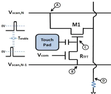
Fig. 1 shows the proposed touch sensing unit consisted of one TFT, one capacitor, and one resistor. The gate electrode of the TFT is connected to the capacitor and resistor. The th scan pulse, , is fed to the gate electrode through the RC circuit. Moreover, the drain electrode is connected to the th scan line and fed by , and the source electrode is connected to the readout circuit. Comparing to the previously proposed circuit [9], [10], it further omits a vertical bus of from the pixel, which make the new circuit more suitable for the in-cell touch sensing. The simple circuit can decrease the consumption of aperture ratio and increase the transmission.
In operation, when the panel is untouched, the scan pulse is firstly fed to node B and raise the voltage of node B, , to 10 V. At this time, the TFT does not output cur-rent because there is no voltage difference between drain and source. Then, although the scan pulse comes in and
Fig. 1. Proposed 1T1R1C touch sensing circuit.
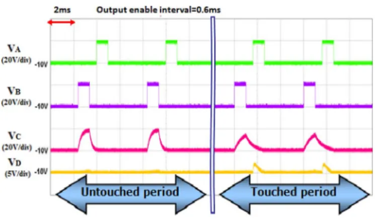
Fig. 2. The measured result of the proposed circuit.
raises the voltage of node A, , to make a voltage difference between drain and source, the has fallen in time to 10 V to turn off the TFT. On the other hand, if touch of pressure in-creases the sensing capacitance, which consequently inin-creases RC time-constant, the scan pulse gets a distortion when it reaches the gate of TFT. Therefore, it needs more time to lower the voltage from 10 V to 10 V. When the scan pulse rapidly raises from 10 V to 10 V, a transient ON cur-rent is produced by the pulse overlapping.
For a good design, the transient ON current should occur only when the selected sensing pixel circuit is touched. To avoid false current, we introduce a time interval, , between two con-secutive gate pulses, which ensure can get back to 10 V before starts rising. avoids the intrinsic distortion owing to the parasitic RC influence on row bus in the large area active matrix. Fig. 2 presents the measured result of the pro-posed pixel circuit built by discrete components. For this simple demonstration, a readout resistor is used to transfer the current signal to voltage signal. The readout resistor is connected to 10 V, which is the same with the scan low voltage. It is note-worthy that the distortion on without touch is resulted from the parasitic capacitance and resistance of the transistor. The
B. Circuit Advantages
One of the values of the proposal is universal to the back-plane structure, such as on-cell and in-cell, and the TFT ma-terial, such as amorphous silicon (a-Si), low temperature poly-crystalline silicon (LTPS), and oxide TFT. Although the design results are different, the effective circuit and the design proce-dures are the same. For example, the obvious difference for the two structures is the sensing capacitor fabrication. In the on-cell structure, the touch sensing array can be fabricated individually and then attached to the display panel. In this case, the sensing capacitor can be formed by the cover glass sandwiched in be-tween finger and the electrode fabricated in the touch sensing array and protected by the cover glass. On the other hand, in the in-cell structure, the capacitor in this RC circuit can be the liquid crystal capacitance (Clc), which is formed by the elec-trodes made on the TFT substrate and the common electrode on the color filter substrate. The Clc can be increased by the ex-ternal forcing to compress the gap of the two electrodes [6], [7]. However, although the capacitor fabrications are different, the capacitance can be proper calculated and simulated.
Moreover, the in-cell types of touch panel which detects the change in the liquid crystal capacitance [6], [7] usually have two disadvantages. One is that, the amplifying TFT outputs large current even in the case without touch and thus keep consuming power whether pixels are touched or not. The other issue is the threshold voltage shift of TFT. Although the uniformity of a-Si TFT is excellent, the device variation of other type TFTs in-cluding LTPS or oxide TFT could affect the circuit performance. In addition, the threshold voltage of TFT would shift under elec-trical stress of usage. In a sensing array, different sensing pixels on the vertical line share the same readout circuit. Because of the threshold voltage variation of the TFTs in different sensing pixels, touch signal and untouched signal in different pixels could be harder to distinguish by the same readout circuit.
The proposed circuit only output current when the selected pixel is touched so that the power consumption could be re-duced. Furthermore, the effect of threshold voltage variation on the proposed circuit can be avoided, as shown by the simulation result in Fig. 3. We use the same TFTs size and charge integrator to perform the simulation. As can be seen, there still is a 0.4 V difference between touched signal and untouched signal when threshold voltage shifts 5 V in one pixel but 5 V in another pixel. In our design, the output signal is more dependent on the overlapping time of the pulses than the threshold voltage of the
Fig. 3. Verification of the threshold voltage variation of the TFT. (a) Pixel 1 and pixel 2 illustrate touch and untouched cases, respectively. (b) Simulation result indicates that the proposed circuit is able to distinguish the sensing difference even when the threshold voltage of the TFT is 5 V.
TFT. This provides the big tolerance of the threshold voltage variation.
C. Demonstration
In this paper, we only demonstrate the design process from the concept to the circuit for the on-cell case, while the case of in-cell can be similarly developed. Fig. 4 shows a demonstration of the proposed circuit in a 2-inch 9 9 array. In this demonstra-tion, a transistor with a proper fixed gate bias, namely, is used to replace the resistor. The alternative pixel circuit is shown in Fig. 5. Besides, the voltage bias for in every sensing pixel is fixed, so it can be provided by . By doing this, it is practical in fabrication to save more aperture area than imple-menting the resistor with a long metal wire.
III. LARGE-AREAPANELSIMULATION
In this section, we design a 42-inch amorphous silicon (a-Si) active touch panel using the proposed circuit and discuss the problems arise from the large size.
A. Design Consideration, Procedure, and Results
There are many factors to design the large-area panel of the proposed sensing method, such as bus line width, size of TFTs, and sensing capacitance. For example, to make the sensing area
Fig. 4. A demonstration of the 2-inch touch panel.
Fig. 5. The alternative touch sensing circuit in which the transistor with a fixed gate bias replaces the resistor component in the RC low-pass filter.
becomes larger, the scan line width can be made thinner but it will cause a large parasitic resistance on the scan line and thus a serious RC time constant delay. The delayed scan pulse at scan far end might result in a false touch signal. When this case happened, the same readout setting cannot be applied at both scan near and far ends. On the contrary, if the scan line width is designed to be wide, it squeezes the area of sensing region. In such a case, the small sensing area corresponding to the small sensing capacitance may not make large difference in the RC time constant between the cases of touched and untouched. An-other example is the size of and the driving TFT. Increase in the driving TFT size can improve the ability to charge the data bus and the read out circuit, while the gate capacitance of TFT increases accordingly. Therefore, the difference of total capac-itance at sensing node when pixel is touched or untouched is less significant, and the intrinsic RC time constant delay of scan pulse increases.
Due to these intertwined design factors, a design procedure is proposed to support our task, as shown in Fig. 6. It contains the following steps.
Step 1) Specify panel size, aspect ratio, and resolution. Step 2) Design line width of scan and data line.
Fig. 6. Flow chart of design procedure.
TABLE I
SPECIFICATION OF THEDESIGNED42 inch TOUCHPANEL
Step 3) Calculate the area of sensing region, which value is the area of one pixel pitch subtracting the area of bus line and TFTs of one pixel. For a fast estimation, the area of TFTs is ignored because it is much smaller than the area of bus line. The value of sensing ca-pacitance can be calculated accordingly.
Step 4) Design sizes of both driving TFT and . Step 5) Calculate the parasitic capacitances and resistances
on the buses.
Step 6) Verify the design with SPICE simulation.
The design procedure is repeated until the design passes the criteria concerning the significant voltage difference between touch and untouched. In this paper, the target of our design is to produce a voltage difference larger than 0.2 V, which is good enough for a common voltage comparator in the periph-eral readout circuit to judge the touch event. Table I lists our final design results.
B. Four-Corner Simulation
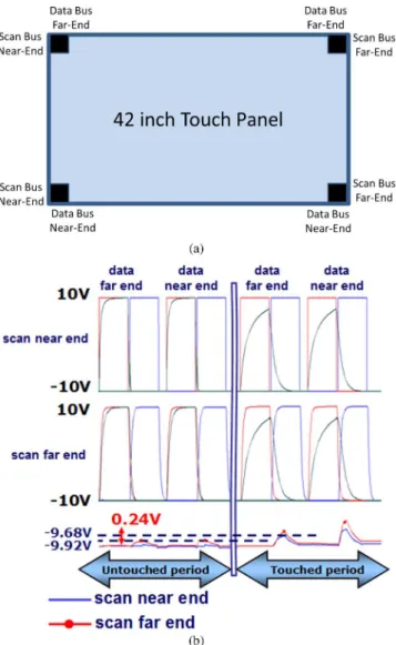
Since the large touch panel suffers from serious parasitic ca-pacitance and resistance on the scan and data buses, the intrinsic RC delay of these buses can possibly make the sensing pixel fail. Therefore, the simulations were conducted for the four pixels of the four corners of the designed 42 inch touch panel. The sim-ulation results shown in Fig. 7 include the scan pulses and the output signals of the four pixels when they are touched and un-touched. The output signal of the pixel at the scan far end is larger than that at the near end owing to the intrinsic bus delay. The output signal from the pixel at data near end is larger than
Fig. 7. (a) Locations of four corners in the panel. (b) Four corners simulation result of the designed 42-inch touch panel using the proposed 2T1C circuit.
that from the data far end, because the current signal from the data far end has to pass through the parasitic resistances and ca-pacitances of the data bus, while the current from the pixel at the data near end comes out directly. For the worst cases, the smallest touched signal appears at scan near end and data far end, and the largest untouched signal appears at scan far end and data near end. The worst-case difference is shown by the two dash lines of the output signal in Fig. 7. This difference be-tween the touched and untouched signals is still larger than our design target of 0.2 V.
C. Current-Induced Voltage Drop on Scan Bus
There is yet another concern of the proposed circuit that when many pixels on the same scan line are touched simultaneously, every touched pixel drains current from the scan bus. This is not an issue for the previously proposed circuits [9], [10], since the sensing current comes from the individual voltage bias buses in column. The total sensing current drained from the same scan bus in row flowing through resistances of scan bus results in the voltage decrease of the scan pulse. In this case, we need to confirm the circuit can still function when the heavy load of multi-touch happens.
Fig. 8. (a) 3T1C circuit without voltage drop on the scan bus for the simulation of multi-touch situation. (b) 2T1C circuit with voltage drop on the scan bus for the simulation of multi-touch situation.
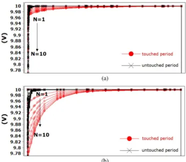
The pixel circuits of 3T1C and 2T1C shown in Fig. 8(a) and 8(b), respectively, were simulated for the two cases without and with the voltage drop on the scan bus. The 2T1C and 3T1C circuits shown in Fig. 8 are the alternative circuits of 1T1R1C and 2T1R1C circuit, respectively. The 2T1R1C circuit is previously proposed in [9]. For the both circuits in a row of 10 and with all the pixels touched simultaneously, the simulation results of the scan pulse high voltage are shown in Fig. 9(a) and 9(b), accordingly. It can be observed that there is more decrease of scan pulse high voltage in 2T1C circuit than in 3T1C circuit. However, the decrease is as small as 0.22 V.
We simulate the worse situation that when the scan pulse high voltage decreases from 10 V to 7 V, which corresponds to hun-dreds of pixels on the same scan line are touched simultane-ously. The result is shown in Fig. 10. It can be seen that the minimum touched signal is still larger than the maximum un-touched signal for 0.2 V, which still meets the design target. The
Fig. 9. Simulation result of pulse high of multi-touch situation: (a) with 3T1C circuit and (b) with 2T1C circuit.
Fig. 10. Four corners simulation result of 2T1C circuit when pulse high de-crease.
concern of voltage drop owing to multi-touch on the scan bus for the large area panel can be relieved.
IV. CONCLUSION
A simple but novel concept of pulse overlapping detection for the active matrix touch panel is proposed. The proposed circuit has many advantages. Firstly, the output signal of the transient on current of TFTs is significant and thus can be easily readout by low cost ICs. Secondly, current signal only occurs when a pixel is touched. The power consumption in operation is greatly reduced. Moreover, device variation can be tolerated, which is the major advantage over the other active touch panels of the source follower type. A 42 inch touch panel of the proposed method is successfully designed. The proposed circuit can pro-vide an excellent way of implementing large area active matrix touch panels.
Takahashi, R. H. Berkeley, N. D. Kim, and S. S. Kim, “12.1-inch a-Si:H TFT LCD with embeded touch screen panel,” in SID Symp. Dig. Tech.
Paper, 2008, vol. 39, no. 1, pp. 830–833.
[5] G. J. A. Destura1, J. T. M. Osenga, and S. J. van der Hoef, “Novel touch sensitive in-cell AMLCD,” in SID Symp. Dig. Tech. Paper, 2004, vol. 35, no. 1, pp. 22–23.
[6] H.-S. Park, Y.-J. Kim, and M.-K. Han, “Touch-sensitive active-matrix display with liquid-crystal capacitance detector arrays,” Jpn. J. Appl.
Phys., vol. 49, no. 3, p. 03CC01, 2010.
[7] C. S. Kim, B. K. Kang, J. H. Jung, M. J. Lee, H. B. Kim, S. S. Oh, S. H. Jang, H. J. Lee, H. Kastuyoshi, and J. K. Shin, “Active matrix touch sensor perceiving liquid crystal capacitance with amorphous silicon thin film transistors,” Jpn. J. Appl. Phys., vol. 49, no. 3, p. 03CC03, 2010.
[8] N. D. Young, G. Harkin, R. M. Bunn, D. J. McCulloch, R. W. Wilks, and A. G. Knapp, “Novel fingerprint scanning arrays using polysilicon TFT’s on glass and polymer substrates,” IEEE Electron Device Lett., vol. 18, no. 1, pp. 19–20, Jan. 1997.
[9] L.-S. Chou, H.-L. Chiu, K.-T. Lin, and Y.-H. Tai, “Active matrix touch sensor detecting time-constant change implemented by IGZO TFTs,” in SID Symp. Dig. Tech. Paper, 2011, vol. 42, no. 1, pp. 1841–1844. [10] Y.-H. Tai, H.-L. Chiu, and L.-S. Chou, “Active matrix touch sensor
de-tecting time-constant change implemented by dual-gate IGZO TFTs,”
Solid-State Electron., vol. 72, no. 6, pp. 67–72, 2012.
Hao-Lin Chiu received the B.S. degree in electrophysics from National Chiao Tung University, Taiwan, in 2004, the M.S. degree in electro-optical engineering in National Chiao Tung University, Taiwan, in 2006, and i s now working toward the Ph.D. degree at the same university.
His current research interests include the sensor and applications of a-Si and a-IGZO TFTs.
Lu-Sheng Chou received the B.S. degree in physics from National Sun Yat-Sen University, Taiwan, in 2008, and is currently working toward the Ph.D. degree in electro-optical engineering in National Chiao Tung University, Taiwan.
His current research interests include the sensor and applications of a-Si and a-IGZO TFTs.