Effects of TaN Substrate Pretreatment by Ar Plasma
on Copper Chemical Vapor Deposition
Cheng-Li Lin,zPeng-Sen Chen, and Mao-Chieh Chen
*
Department of Electronics Engineering and Institute of Electronics, National Chiao-Tung University, Hsinchu 300, Taiwan
CVD Cu films deposited on TaN substrates with and without an Ar plasma treatment prior to Cu film deposition and the effects of postdeposition thermal annealing were investigated. Cu films deposited on an Ar-plasma-treated TaN substrate have a number of favorable properties over the films deposited on a TaN substrate without the plasma treatment. These include a smoother film surface, regular arrangement of Cu grains, and increased共111兲-preferred orientation. The postdeposition thermal annealing en-hanced the共111兲-preferred orientation and decreased the resistivity of the as-deposited Cu films. As the results of Ar plasma substrate pretreatment, we presume that the smoother and amorphous-like surface layer of the TaN substrate enhanced the formation of the most stable共111兲 texture Cu films, and that the higher substrate surface energy resulted in Cu films with smoother surface and regularly shaped smaller grains. Thus, a combined process including Ar plasma substrate treatment prior to Cu film deposition and postdeposition thermal annealing at an appropriate temperature in N2ambient is proposed for the advantages of low-resistivity and high共111兲-oriented Cu film deposition.
© 2002 The Electrochemical Society. 关DOI: 10.1149/1.1462794兴 All rights reserved.
Manuscript submitted June 26, 2001; revised manuscript received November 22, 2001. Available electronically March 20, 2002.
As integrated circuits advance into deep sub-quarter-micrometer regime, the conventional Al-based interconnect scheme is faced with various performance and reliability challenges, such as interconnect propagation delay and the problem of electromigration.1,2Therefore, other metals with a lower electrical resistivity and superior elec-tromigration resistance are needed to replace Al as the interconnect material. Copper has been regarded as a potential candidate to re-place Al and its alloys for multilevel interconnection applications because of its low bulk resistivity 共1.67 ⍀ cm兲, excellent elec-tromigration resistance, and high resistance to stress-induced voids.3,4 There are various techniques for copper film deposition, such as chemical vapor deposition共CVD兲,5,6conventional as well as ionized metal plasma共IMP兲, physical vapor deposition 共PVD兲,7and electrochemical deposition共ECD兲 including electroplating and elec-troless plating;8,9among these, the CVD method has the advantages of superior step coverage and excellent gap-filling capability for high-aspect-ratio vias and trenches,6making it the most promising Cu film deposition technique for future integrated circuit共IC兲 appli-cations. Since it is difficult to pattern the Cu film by dry etch meth-ods, the Cu damascene process is developed to cope with this diffi-culty. The dual damascene process on scaled-down devices requires perfect gap-filling capability of copper for high-aspect-ratio vias and trenches. Although the Cu ECD combined with IMP of a thin Cu seed layer and barrier layers provides a suitable solution for IC technologies above 0.25m, deposition techniques for a conformal and continuous thin barrier as well as a conformal and void-free Cu film filling into deep sub-quarter-micrometer vias, such as CVD, are eventually unavoidable for future-generation devices.10A number of barrier materials have been used as substrates for CVD of Cu films, such as W, Ti, TiN, Ta, and TaN;5,11-13among them, TaN exhibits a superb barrier capability against Cu diffusion.14 However, the chemically vapor-deposited Cu films on TaN substrate exhibited a fairly low-peak-ratio of Cu共111兲/Cu共200兲 preferred orientation in the X-ray diffraction共XRD兲 spectrum,5,13which is unfavorable for elec-tromigration resistance. Since the nucleation process and the micro-structure of Cu films are very sensitive to the substrate surface conditions,15,16 it has been reported that plasma treatment on the substrate surface prior to the Cu film deposition results in deposited films with preferred共111兲 texture.17,18
In this work, effects of TaN substrate pretreatment by Ar plasma
on copper CVD were investigated using a multichamber low-pressure CVD system. The effects of postdeposition thermal anneal-ing were also investigated.
Experimental
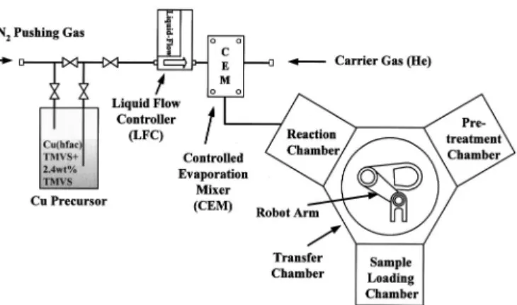
Figure 1 shows a schematic of the multichamber Cu CVD appa-ratus built for this study. The appaappa-ratus consists of a cluster of four chambers and a direct liquid injection共DLI兲 system for precursor delivery. The chamber cluster is composed of a sample-loading chamber共for samples loading/unloading兲, a pretreatment chamber, a reaction chamber, and a transfer chamber. The pretreatment chamber is used to preclean and/or modify the substrate surface by plasma treatment. CVD of Cu films is to be carried out in the reaction chamber. The transfer chamber, which houses a robot arm, is de-signed to handle the transfer of a sample to and from each chamber. In the reaction chamber there is a shower-head injector through which the Cu precursor is introduced into the reaction chamber in a stream of carrier gas. Under the injector, there is a substrate suscep-tor that can be heated by a resistive heating element up to a maxi-mum temperature of 400°C. The susceptor is also rotatable for better uniformity of film deposition. The shower-head injector is moveable in the vertical direction so that the distance between the injector and the sample can be adjusted. The sidewall of the reaction chamber and the precursor injector are kept at a temperature of 45°C by the circulation of warm water to prevent Cu deposition of precursor condensation.
*Electrochemical Society Active Member. zE-mail address: cllin.ee85g@nctu.edu.tw
Figure 1. Schematic of multichamber Cu CVD apparatus built for this study.
The Cu precursor used in this study is Cu 共1,1,1,5,5,5-hexa-fluoroacetylacetonate兲trimethylvinylsilane 关Cu共hfac兲TMVS兴 with 2.4 wt % TMVS additive.19-21The 2.4 wt % TMVS enhances the stability of the precursor.21The liquid Cu precursor is delivered by the DLI system consisting of a liquid flow controller共LFC兲 and a controlled evaporation mixer 共CEM兲 共Fig. 1兲. Initially, the liquid precursor is propelled by N2gas through the LFC. It is then vapor-ized in the CEM and mixed with the carrier gas. Helium共He兲 is used as the carrier gas in this study. The precursor-saturated carrier gas is introduced into the reaction chamber through the gas injector.
In this work, TaN was used as the substrate for the CVD of Cu films. TaN layers of 50 nm thickness were sputter-deposited on a thermal-oxide共500 nm thickness兲-covered Si wafer. A dc magnetron sputtering system with a base pressure of 1.5⫻ 10⫺6Torr was used to reactively sputter a Ta target 共99.99% purity兲 in an Ar/N2 gas mixture at a pressure of 7.6 mTorr for TaN film deposition. The flow rates of Ar and N2were 24 and 6 sccm, respectively, for making the gas mixture, and the TaN films were sputter-deposited at a power of 150 W. The TaN-coated substrate wafer was loaded into the multi-chamber Cu CVD system. When the pressure of the sample-loading chamber reached 10⫺6 Torr, the substrate wafer 共together with the substrate holder兲 was transferred to the pretreatment chamber or reaction chamber via the transfer chamber depending on the process requirement of whether the plasma pretreatment on substrate was to be performed or not. In this study, Ar plasma treatment was per-formed at 50 W power for 10 min under the following conditions: Ar flow rate 6 sccm, gas pressure 40 mTorr, substrate temperature 80°C, and self-dc bias⫺270 V. After the plasma pretreatment, the sample was transferred to the reaction chamber for Cu film deposi-tion. Prior to Cu film deposition, the substrate sample was heated to the desired deposition temperature with He carrier gas flowing at 25 sccm and the chamber pressure maintained at 150 mTorr. Usually, approximately 1 h is required for the substrate sample to reach the preset temperature. In this study, Cu CVD was performed over a temperature range of 120-240°C at a pressure of 150 mTorr with a precursor flow rate of 0.4 mL/min and a He carrier gas flow rate of 25 sccm. Major processing conditions and the parameters of the Cu CVD system used in this study are summarized in Table I. At the end of Cu film deposition, the sample was cooled in the ambient of He at a pressure of 150 mTorr.
The thickness of Cu films was measured using a DekTek profiler on the patterned Cu films and was verified by cross-sectional scan-ning electron microscopy共SEM兲. SEM was also used to observe the
surface morphology of the deposited Cu films and cross-sectional views of copper nucleated on TaN substrate. A four-point probe was employed to measure the sheet resistance. Auger electron spectros-copy 共AES兲 was used to analyze the impurity content in the Cu films. The crystal structure was identified by XRD analysis. The surface roughnesses of the Cu and substrate TaN films were evalu-ated by atomic force microscopy共AFM兲. Rutherford backscattering spectroscopy共RBS兲 was used to determine the composition of the TaN substrate samples.
Results and Discussion
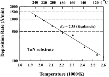
CVD Cu films on TaN substrates.—Cu films were chemically vapor deposited on reactively sputtered TaN substrates, which have a resistivity of 0.6 m⍀ cm and a composition of TaN1.2, as deter-mined by RBS. Figure 2 shows the deposition rate of Cu films as a function of substrate temperature共Arrhenius plot兲 at a constant pres-sure of 150 mTorr with a He carrier gas flow rate of 25 sccm and a liquid Cu precursor flow rate of 0.4 mL/min. Since the chemical reaction of Cu CVD involves basically a thermal dissociation of the Cu precursor, a higher temperature would result in a higher rate of deposition. The activaton energy Eawas determined to be 7.35 kcal/ mol by the Arrhenius equation
R⫽ R0 exp共⫺Ea/kT兲 关1兴
where R is the deposition rate, R0is the Arrhenius pre-exponential constant or frequency factor, k is the Boltzmann constant, and T is the absolute temperature. Other values of activation energy were reported in the literature, e.g., the values of 10.20 kcal/mol 共depos-ited on W substrates at 0.5 Torr兲,2216.70 kcal/mol共deposited on TiN substrates at 10.5 Torr兲,2319.30 kcal/mol共deposited on Ta substrates at 1.5 Torr兲,5 and 17.90 kcal/mol共deposited on TiN substrates at 0.5 Torr兲.21The difference in the values of the activation energy is presumably due to different deposition conditions.
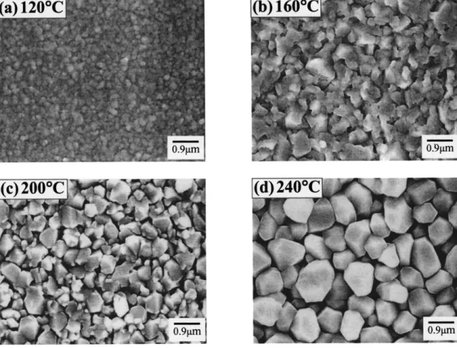
The SEM micrographs in Fig. 3 show the surface morphology of copper films deposited at various temperatures for a deposition time of 10 min. The grain size of Cu increases with the deposition tem-perature. At higher deposition temperatures 共200-240°C兲, the Cu films exhibit stacked grains featuring clear boundaries as well as voids between large grains. Figure 4 shows the grain size of Cu increasing with the deposition temperature. The resistivity of Cu films was calculated using the measured sheet resistances and film thicknesses. Figure 5 illustrates the resistivity of Cu films as a func-tion of deposifunc-tion temperature at a deposifunc-tion pressure of 150 mTorr. It has been reported that the resistivity of CVD Cu films is closely related with the impurity content and microstructure.24,25 The slightly higher resistivity at low deposition temperatures is presum-Figure 2. Deposition rate vs. substrate temperature 共Arrhenius plot兲 at a
constant pressure of 150 mTorr for TaN substrate.
Table I. Processing conditions for multichamber Cu CVD sys-tem.
Pretreatment chamber
共Ar plasma operating
conditions兲 Reaction chamber 共Cu film deposition conditions兲 Substrate temperature 共°C兲 80 Substrate temperature共°C兲 120-240 Operating pressure
共mTorr兲 40 Operating pressure共mTorr兲 150
Ar gas flow rate
共sccm兲 6 Cu precursor flow rate共mL/min兲 0.4
RF power
共W兲 50 CEM temperature共°C兲 70
Self-dc bias
共V兲 ⫺270 Carrier gas 共He兲 flowrate共sccm兲
25 Pretreatment
time共min兲
10 Substrate holder rotation speed共rpm兲
10 Gas-injector/susceptor
distance共cm兲
2 Delivery line temperature
共°C兲 72
Reactor wall temperature
共°C兲 45
Journal of The Electrochemical Society, 149共5兲 C237-C243 共2002兲 C238
ably due to higher contamination of residual impurities from the reaction by-products, while the high resistivity at high deposition temperatures results from the higher contamination of impurities in the film as well as the porous film structure. The most appropriate temperature for Cu film deposition from the viewpoint of low resis-tivity under the present deposition condition appears to be around 160°C共2.30 ⍀ cm兲. Figure 6 illustrates the AES depth profiles of CVD Cu films deposited on TaN substrates. The most notable
im-purities contaminated in CVD Cu films are carbon共C兲 and oxygen
共O兲, which may result from incomplete desorption of hfac ligand
during the CVD process.25
Nucleation and surface morphology observation.—The surface conditions of substrates play an important role in the CVD of Cu films. Figure 7 shows AFM images of the TaN substrate before and after Ar plasma treatment at 50 W for 10 min. The Ar plasma treat-Figure 3. SEM micrographs showing surface morphology of Cu films deposited on TaN substrates at temperatures of共a兲 120, 共b兲 160, 共c兲 200, and 共d兲 240°C. The films were deposited at a constant pressure of 150 mTorr for 10 min.
Figure 4. Grain size vs. deposition temperature for Cu films deposited at a
constant pressure of 150 mTorr for 10 min.
Figure 5. Resistivity of Cu film vs. deposition temperature for Cu films
ment significantly improved the surface smoothness of the TaN sub-strate. In order to study the effect of substrate pretreatment by Ar plasma, the nucleation process of Cu films was investigated. Figure 8 illustrates the cross-sectional view SEM micrographs for Cu nucleation on TaN substrates with and without an Ar plasma treat-ment. On a TaN substrate without Ar plasma treatment, the initial 1 min deposition resulted in Cu grains of spherical shape with a wet-ting angle共contact angle兲 of about 70° 共Fig. 8a兲, similar to Al nucle-ation on TiN substrates reported in the literature.26 On the Ar-plasma-treated TaN substrate, the Cu grains show a flat-dome shape with a wetting angle of about 42°共Fig. 8b兲; after 2 min deposition, the grains grew and became larger in size, but the grain shape re-mained basically unchanged 共Fig. 8c兲. According to Young’s equation18,27
cos ⫽ s⫺ i
c 关2兴
where is the wetting angle 共contact angle兲 of the copper grain, s andcare the respective surface energy of the TaN substrate and the Cu grain, andiis the interfacial energy between the Cu grain and the TaN substrate. The smaller wetting angle of 42° indicates that the Ar-plasma-treated TaN substrate has a higher substrate surface Figure 6. AES depth profiles of Cu films deposited on TaN substrates
共with-out plasma treatment prior to Cu deposition兲.
Figure 7. AFM images showing surface morphology of TaN substrates共a兲 without plasma treatment and共b兲 with Ar plasma treatment 共at 50 W with 40 mTorr pressure for a plasma time of 10 min兲.
Figure 8. SEM micrographs showing cross-sectional view of copper grains on TaN substrates:共a兲 without plasma treatment 共after 1 min deposition time兲, 共b兲 with Ar plasma treatment 共after 1 min deposition time兲, and 共c兲 with Ar plasma treatment共after 2 min deposition time兲.
Journal of The Electrochemical Society, 149共5兲 C237-C243 共2002兲 C240
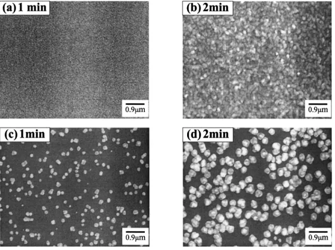
energy or lower interfacial energy, thus enhancing the Cu films growth by two dimensions 共layer growth兲 and forming the most stable 共111兲 closely packed configuration.18,28 Moreover, the Cu-containing adspecies tend to nucleate uniformly on the Ar-plasma-treated TaN substrate. A similar result was reported for the CVD Al nucleation on a SiO2-coated substrate pretreated by H2 plasma.29 Figure 9 shows top-view SEM micrographs for the nucleation pro-cess of Cu films deposited at 160°C on a TaN substrate with and without an Ar plasma treatment. On the Ar-plasma-treated TaN sub-strate, the Cu-containing adspecies关Cu共hfac兲兴 easily and uniformly nucleated on the substrate surface, forming dense and small Cu nu-clei after 1 min deposition共Fig. 9a兲. The Cu-containing adspecies continuously adsorbed on the surface of Cu nuclei to proceed with the growth of copper nuclei, resulting in larger Cu grains and a continuous Cu film after 2 min deposition共Fig. 9b兲. On the TaN substrate without Ar plasma treatment, the Cu-containing adspecies were sparsely nucleated on the substrate surface, and the subsequent adspecies tend to nucleate on the existing Cu nuclei rather than the TaN substrate. As a result, the Cu nuclei grew into Cu grains sparsely distributed on the substrate, while a few new Cu nuclei also randomly nucleated directly on the TaN substrate, forming smaller Cu grains共Fig. 9c兲. After 2 min deposition, all grains grew larger, though a few new smaller grains are scattered among the larger ones
共Fig. 9d兲. A similar result was reported in the literature that the
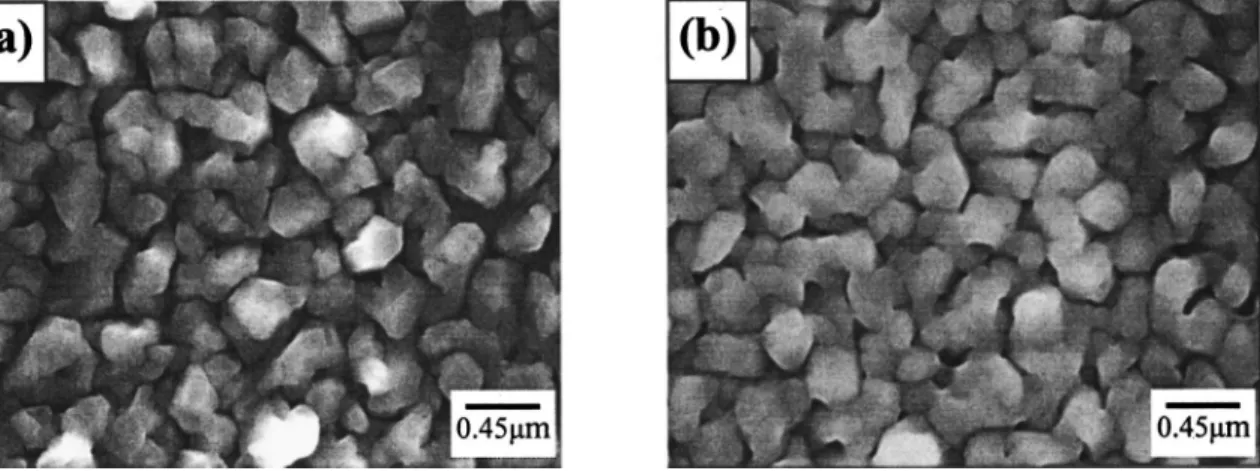
nucleation of Cu on the H2-plasma-treated TiN substrate led to a dense distribution of Cu grains.30The SEM micrograph in Fig. 10 shows the surface morphology of a Cu film deposited at 160°C for 10 min on the Ar-plasma-treated TaN substrate. In comparison with the corresponding Cu film deposited on the TaN substrate without Ar plasma treatment 共Fig. 3b兲, the surface morphology of the Cu film deposited on the Ar-plasma-treated TaN substrate reveals
regu-larly shaped smaller grains. As a result, better surface smoothness is expected for the Cu film deposited on the Ar-plasma-treated TaN substrate. This is evidenced by the results of AFM analysis shown in Fig. 11. The Cu film deposited on the TaN substrate without Ar plasma treatment shows irregular Cu grains with an average surface roughness关root-mean-square 共rms兲兴 of 55.9 nm, while the Cu film deposited on the Ar-plasma-treated TaN substrate shows much regu-lar and smaller grains with an average surface roughness 共rms兲 of 32.8 nm.
Figure 9. SEM micrographs showing Cu nucleation at 160°C for共a兲 1 and 共b兲 2 min deposition on TaN substrate with Ar plasma treatment, and 共c兲 1 and 共d兲 2 min deposition on TaN substrate without plasma treatment.
Figure 10. SEM micrographs showing surface morphology of Cu film de-posited on TaN substrate with Ar plasma treatment prior to Cu deposition. The Cu film was deposited at 160°C and 150 mTorr for 10 min.
The thicknesses of the Cu films with and without an Ar plasma substrate pretreatment are 348 and 408 nm, respectively, for a 10 min deposition at a substrate temperature of 160°C. The thinner Cu film on the Ar-plasma-treated TaN substrate is presumably due to the regular arrangement of smaller Cu grains, which in turn results in a denser microstructure and a smaller film thickness. The resistivity of the Cu film deposited on the Ar-plasma-treated TaN substrate was determined to be 3.40⍀ cm, which is higher than that of the Cu film deposited on the substrate without the plasma treatment共2.30
⍀ cm兲, presumably due to the smaller Cu grains and thus a higher
boundary density.
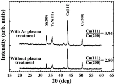
Preferred orientation and postdeposition thermal anneal-ing.—The preferred orientation of Cu films is also affected by the Ar plasma treatment on the TaN substrate. Figure 12 shows the XRD spectra for Cu films deposited on TaN substrates with and without an Ar plasma treatment. It can be seen that the intensity peak ratio of Cu共111兲 to Cu共200兲 diffraction signals increased from 2.80 to 3.94 resulting from the Ar plasma treatment on the TaN substrate. With Ar plasma treatment, the smoother and thin amorphous-like TaN substrate surface enabled the migration of Cu-containing adspecies to the most stable site to forming a 共111兲 preferential orientation because the共111兲 texture is the most stable configuration.18,28
Copper films deposited on the TaN substrate were thermally an-nealed at 400°C for 30 min in an N2ambient. Figure 13 shows the surface morphology of Cu films deposited on Ar-plasma-treated sub-strates before and after a thermal annealing. The thermally annealed Cu film reveals a closer contact between Cu grains, similar to those reported in the literature for CVD Cu films annealed in Ar and Ar/H2ambients.31Moreover, thermal annealing also resulted in de-crease in film resistivity as well as inde-crease in intensity peak ratio of Cu共111兲 to Cu共200兲 diffraction signals, as shown in Table II. The decrease in film resistivity is presumably due to the closer contact
between the Cu grains. In addition, we presume that the Cu film deposited on the Ar-plasma-treated substrate possesses a uniform surface energy and little variation of film stress because of the better regular arrangement of Cu grains. As a result, thermal annealing would reduce the grain boundary and surface energy of the Cu film, resulting in the recrystallization of Cu grains to forming the most stable 共111兲 texture.18,32On the other hand, Cu grains of different sizes are irregularly arranged for the Cu film deposited on the TaN substrate without a plasma treatment; thus, there is nonuniform sur-face energy and nonuniform films stress, and this nonuniformity would be reduced in order to reduce the total system energy during thermal annealing.32As a result, there is not enough driving force to recrystallize the Cu grains for the formation of the most stable共111兲 texture, and the improvement of the Cu共111兲/Cu共200兲 intensity peak ratio was relatively moderate as compared with the Cu film depos-ited on the Ar-plasma-treated substrate. A similar observation was also reported for CVD Cu films thermally annealed at 450°C in Ar and Ar/H2ambients.31With regard to adhesion of Cu films, a Scotch tape pulling test was used to qualify the adhesion between the CVD Cu films and the TaN substrates. All samples with the Cu film de-posited at 160°C and 150 mTorr, irrespective of substrate pretreat-ment by Ar plasma and/or post thermal annealing, passed the Scotch tape test. In summary, we conclude that the smoother TaN substrate surface with a higher surface energy resulting from the Ar plasma treatment, is responsible for the improvement of various Cu film properties.
Conclusion
The CVD Cu films deposited on TaN substrate with and without an Ar plasma pretreatment and the effect of postdeposition thermal annealing were investigated. The Cu films deposited on the Ar-plasma-treated TaN substrate have a number of favorable properties over the films deposited on the TaN substrate without the plasma treatment. These include a smoother film surface, regular arrange-ment of Cu grains, and enhanced 共111兲 preferential orientation. However, the Cu films deposited on the Ar-plasma-treated substrate have a higher electrical resistivity, presumably due to smaller grain size, and thus higher grain boundary density. Postdeposition thermal annealing resulted in the reduction of electrical resistivity and an increase of the Cu共111兲/Cu共200兲 diffraction peak ratio. As a result of Ar plasma substrate pretreatment, we presume that the smoother and amorphous-like surface layer of the TaN substrate enhanced the for-mation of the most stable 共111兲-oriented Cu films, and that the higher substrate surface energy resulted in Cu films with a smoother surface and regularly shaped smaller grains. A combined process is proposed for the advantages of low resistivity and high 共111兲-Figure 11. AFM images showing surface morphology of Cu films deposited
on TaN substrates 共a兲 without plasma treatment and 共b兲 with Ar plasma treatment prior to Cu deposition.
Figure 12. XRD spectra of Cu films deposited on TaN substrates with and
without Ar plasma treatment prior to Cu deposition. Journal of The Electrochemical Society, 149共5兲 C237-C243 共2002兲
oriented Cu film deposition. First, the TaN substrate is treated with Ar plasma prior to Cu film deposition, and second, the deposited Cu film is thermally annealed at an appropriate temperature 共e.g., 400°C兲 in an N2ambient.
National Chiao-Tung University assisted in meeting the publication costs of this article.
References
1. A. Jain, A. V. Gelatos, T. T. Kodas, M. J. Hampden-Smith, R. Marsh, and C. J. Mogab, Thin Solid Films, 262, 52共1995兲.
2. C. K. Hu, B. Luther, F. B. Kaufman, J. Hummel, C. Uzoh, and D. J. Pearson, Thin Solid Films, 262, 84共1995兲.
3. A. Jain, T. T. Kodas, R. Jairath, and M. J. Hampden-Smith, J. Vac. Sci. Technol. B,
11, 2107共1993兲.
4. N. Awaya, H. Inokawa, E. Yamamoto, Y. Okazaki, M. Miyake, Y. Arita, and T. Kobayashi, IEEE Trans. Electron Devices, ED-43, 1206共1996兲.
5. R. Kroger, M. Eizenberg, D. Cong, N. Yoshida, L. Y. Chen, S. Ramaswami, and D. Carl, J. Electrochem. Soc., 146, 3248共1999兲.
6. C. H. Lee, K. H. Shen, T. K. Ku, C. H. Luo, C. C. Tso, H. W. Chou, and C. Hsia, 2000 IEEE International Interconnect Technology Conference, p. 242, San Fran-cisco, CA共2000兲.
7. B. Chin, P. Ding, B. Sun, T. Chiang, D. Angelo, I. Hashim, Z. Xu, S. Edelstein, and F. Chen, Solid State Technol., 41, 141共1998兲.
8. R. L. Jackson, E. Broadbent, T. Cacouris, A. Harrus, M. Biberger, E. Patton, and T. Walsh, Solid State Technol., 41, 49共1998兲.
9. Y. Shacham-Diamand and S. Lopatin, Microelectron. Eng., 37Õ38, 77 共1997兲. 10. P. Motte, M. Proust, J. Torres, Y. Gobil, Y. Morand, J. Palleau, R. Pantel, and M.
Juhel, Microelectron. Eng., 50, 369共2000兲.
11. N. I. Cho and Y. Sul, Mater. Sci. Eng., B, 72, 184共2000兲.
12. S. Voss, S. Gandikota, L. Y. Chen, R. Tao, D. Cong, A. Duboust, N. Yoshida, and S. Ramaswami, Microelectron. Eng., 50, 501共2000兲.
13. R. Kroger, M. Eizenberg, D. Cong, N. Yoshida, L. Y. Chen, S. Ramaswami, and D. Carl, Microelectron. Eng., 50, 375共2000兲.
14. M. T. Wang, Y. C. Lin, and M. C. Chen, J. Electrochem. Soc., 145, 2538共1998兲. 15. D. H. Kim, R. H. J. Wentorf, and W. N. Gill, J. Appl. Phys., 74, 5164共1993兲. 16. K. Hanaoka, H. Ohnishi, and K. Tachibana, Jpn. J. Appl. Phys., Part 1, 34, 2430
共1995兲.
17. Y. S. Kim, D. Jung, and S. K. Min, Thin Solid Films, 349, 36共1999兲. 18. K. Kamoshida and Y. Ito, J. Vac. Sci. Technol. B, 15, 961共1997兲.
19. J. A. T. Norman, B. A. Mutamore, P. N. Dyer, D. A. Roberts, and A. K. Hochberg, J. Phys. IV, 1, C2-271共1991兲.
20. J. C. Chiou, Y. J. Chen, and M. C. Chen, J. Electron. Mater., 23, 383共1994兲. 21. T. Nguyen, L. J. Charneski, and S. T. Hsu, J. Electrochem. Soc., 144, 2829共1997兲. 22. A. Jain, K. M. Chi, T. T. Kodas, and M. J. Hampden-Smith, J. Electrochem. Soc.,
140, 1434共1993兲.
23. Y. K. Chae, Y. Shimogaki, and H. Komiyama, J. Electrochem. Soc., 145, 4226 共1998兲.
24. S. S. Yoon, J. S. Min, and J. S. Chun, J. Mater. Sci., 30, 2029共1995兲. 25. P. J. Lin and M. C. Chen, Jpn. J. Appl. Phys., Part 1, 38, 4863共1999兲. 26. M. Avinun, W. D. Kaplan, M. Eizenberg, T. Guo, and R. Mosely, Solid-State
Electron., 43, 1011共1999兲.
27. R. J. Stokes and D. F. Evans, Fundamentals of Interfacial Engineering, p. 59, Wiley-VCH, Inc., New York共1997兲.
28. H. Toyoda, T. Kawanoue, S. Ito, M. Hasunuma, and H. Kaneko, in Stress-Induced Phenomena in Metallization, Third International Workshop, Palo Alto, CA, USA, June 1995, P. S. Ho, J. Bravman, C. Y. Li, and J. Sanchez, Editors, No. 373, p. 169, American Institute of Physics Conference Proceedings, New York共1996兲. 29. A. Weber, U. Bringmann, K. Schiffmann, and C. P. Klages, Mater. Res. Soc. Symp.
Proc., 282, 311共1993兲.
30. J. H. Lee, J. H. Lee, K. J. Hwang, J. Y. Kim, C. G. Suk, and S. Y. Choi, Thin Solid Films, 375, 132共2000兲.
31. S. K. Rha, W. J. Lee, S. Y. Lee, D. W. Kim, C. O. Park, and S. S. Chun, Jpn. J. Appl. Phys., Part 1, 35, 5781共1996兲.
32. C. V. Thompson and R. Carel, Mater. Sci. Eng., B32, 211共1995兲.
Figure 13. SEM micrographs showing surface morphology of Cu film deposited on TaN substrate with Ar plasma treatment prior to Cu deposition共a兲 as-deposited and共b兲 annealed at 400°C for 30 min in N2ambient.
Table II. Effects of thermal annealing „400°CÕ30 min… on Cu films electrical resistivity and diffraction peak ratio of Cu„111…Õ Cu„200….
Ar plasma treatment on TaN substrate
Resisitvity
共⍀ cm兲 diffraction peak ratioCu共111兲/Cu共200兲 As-deposited After anneal As-deposited After anneal No 2.30 2.15 2.80 3.10 Yes 3.40 2.10 3.94 5.14