The Impact of Active Layer Pre-Treatment on Bias Stress Stability of Sol-gel Derived Amorphous Indium-Gallium-Zinc-Oxide Thin Film Transistor
Wan-Fang Chung a,Ting-Chang Chang b, c,Hung-Wei Li d, Yu-Chun Chen b, Iue-Hen Li
a, Tseung-Yuen Tseng a, Ya-Hsiang Tai e
a Department of Electronics Engineering & Institute of Electronics, National Chiao Tung
University, Hsinchu 300, Taiwan, R.O.C.
b Department of Physics, National Sun Yat-Sen University, Kaohsiung 804, Taiwan,
R.O.C.
c Center for Nanoscience & Nanotechnology, National Sun Yat-Sen University,
Kaohsiung 804, Taiwan, R.O.C.
d Department of Photonics & Institute of Electro-Optical Engineering, National Chiao
Tung University, Hsinchu 300, Taiwan, R.O.C.
e Department of Photonics & Display Institute, National Chiao Tung University, Hsinchu
300, Taiwan, R.O.C.
We have investigated the gate bias stress-induced instability on the electrical properties with different pre-treatments for sol-gel derived amorphous indium gallium zinc oxide thin film transistors (a-IGZO TFTs). The device with illuminating and heating pre-treatments under the positive/negative gate bias stress in vacuum had the smallest threshold voltage shift as the stress duration increased, while the device with oxygen gas pre-treatment exhibited an obvious variation. These electrical instabilities were ascribed to the charge trapping in the gate insulator and the oxygen/water adsorption on the active layer. It indicates that the specific pre-treatment for the a-IGZO film can improve the device stability. It also provides the important information for the subsequent passivation process concerning the pre-treatment of the active layer.
Introduction
Recently, zinc oxide (ZnO)-based materials, such as ZnO, indium zinc oxide (IZO), and indium gallium zinc oxide (IGZO), have been investigated as active channel layers in thin film transistors (TFTs) for active matrix organic light-emitting diodes (AMOLED) and active matrix liquid crystal displays (AMLCD), due to potential high transparency and large area deposition applications (1-5). Compared to conventional amorphous silicon (a-Si) TFTs, a-IGZO TFTs have similar device performance. Furthermore, they have the advantage of low manufacturing cost and a compatible process flow with conventional
a-Si TFTs (6,7). Nowadays, amorphous oxide TFTs are mainly produced by vacuum
systems such as radio frequency magnetron sputtering and pulsed laser deposition (1,4,7,8). Their high carrier mobility, low processing temperature and high transparency are advantageous for numerous applications (9). They have also attracted interest as a backplane candidate in large-area applications on account of their highly uniform deposition (10). Therefore, simple solution processing with high throughput and low cost
is desirable for TFT fabrication. Several research groups have demonstrated the sol-gel derived TFTs using ZnO, IZO, and IGZO as active channel layers (11,12). Their results further displayed that the device performance of the sol-gel derived amorphous oxide TFTs is comparable to that of the vacuum-processed oxide TFTs, and demonstrate low-cost potential in mass manufacturing. Among the currently available oxide semiconductors, IGZO generally allows higher field effect mobility and better stability to be obtained (13).
Motivation
The device stability is an important issue in real circuit application. It was reported that the stability of a-IGZO TFTs suffered from several factors, such as the oxygen/water adsorption, temperature, illumination, and applied bias (14-17). We have reported that the electrical degradation under the gate bias stress was mainly contributed by the charge trapping model and the influence of the ambient atmosphere involving the electric field-induced oxygen adsorption (18). In order to obtain the stable electrical characteristics, some pre-treatments were conducted on the active layer and the degradation mechanisms were clearly discussed herein. It would be helpful to provide the information about the pre-treatment for the subsequent passivation process. This paper examines the stability of the gate bias stress on the electrical characteristics of a-IGZO TFTs under some specific pre-treatments.
Experimental Procedure
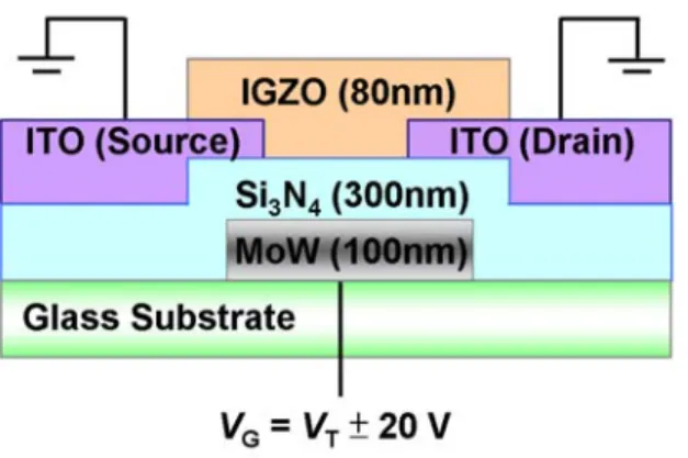
A coplanar type bottom-gate a-IGZO TFT was fabricated on glass substrate in this study. After MoW (100 nm) gate electrode, silicon-nitride (300 nm) gate dielectric and indium tin oxide source/drain electrode formation, an 80-nm-thick a-IGZO thin film was deposited as active layer by spin-coating at room temperature and atmospheric pressure, and then baked in a furnace at 450 °C for 1 h to improve the film quality. It was subsequently patterned by photolithography and wet etching. The precursor solution for
a-IGZO films was synthesized by dissolving 1.0 M of zinc acetate dihydrate
[Zn(CH3COO)2·2H2O], 0.5 M of gallium nitrate hydrate [Ga(NO3)3·xH2O] and 0.5 M of
indium nitrate hydrate [In(NO3)3·xH2O] in 2-methoxyethanol and monoethanolamine
solvent and mixing at 60 °C for 1 h. The a-IGZO TFT was obtained at the compositional ratio of In/Ga/Zn=1:1:2 with the saturation mobility of 1.32 cm2 V-1 s-1, the threshold voltage of 3.32 V, the subthreshold swing of 1.37 V/dec in air. The channel width and length of a-IGZO TFTs were 500 and 30 μm, respectively. The device structure is shown in figure 1.
The DC voltages were applied to the gate electrode of the device for the study of electrical reliability. In order to simulate the a-IGZO TFTs operating under the working mode, the stress condition was set at VG = VT ± 20 V and the stress times was 1000 sec.
The source and drain electrodes were grounded during the stress. The applied voltages of the gate, drain, and source electrodes were also illustrated in figure 1. Variations in the electrical characteristics were monitored from the drain current-gate voltage (IDS-VG). All
the current-voltage (I-V) characteristics of sol-gel derived a-IGZO TFTs with different active layer pre-treatments under positive/negative gate bias were measured at room
temperatures (25 ℃) for the gate voltages VG ranging from -10 V to 20 V with a fixed
Figure 1. Schematic cross section of sol-gel derived a-IGZO TFTs under positive/negative gate bias.
Results and Discussion
In the beginning, the electrical characteristics of a-IGZO TFTs without pre-treatment under the gate bias of VT ± 20 V over a period of 1000 s were shown in figures 2 (a) and
2 (b). Obviously, we observed that the transfer curve of the a-IGZO TFT exhibited a positive shift to 3.23 V under the positive gate bias of VT + 20 V over a period of 1000
sec, which may be ascribed to the charge trapping in the gate dielectric and the electric-field-induced oxygen adsorption. While the electrical curve displayed a tiny negative shift of 0.49 V and a gradually apparent hump phenomenon under the negative gate bias
of VT - 20 V, due to the appearance of positive charged donor states induced by band
bending and multi-channel formation induced by the gas species adsorption (18,19). Literature has reported that oxygen and water in the surrounding atmosphere are known to affect the transistor stability (20,21). As a result, these adsorbing species must be removed from the amorphous oxide to improve the device stability.
Figure 2. Time evolution of ID -VG transfer characteristics curves of a-IGZO TFTs
without pre-treatment under (a) positive and (b) negative gate bias stress. The sweep was done at VD = 10 V.
Two pre-treatment methods were used to remove the adsorbing species. Vacuum pump and pressure-controllable chamber were employed to achieve the pre-treatment concerning the adsorbing species removal. During this treatment, the oxygen and water physically adsorbing on a-IGZO film would be evacuate to the outside ambient. The transfer characteristics under the positive/negative gate bias showed similar behavior with
Besides, the hump phenomenon disappeared as the device was experienced a vacuum pre-treatment, which may be contributed by the gas species desorption. The extracted threshold voltage values are summarized in Table I and Table Ⅱ.
Although the above pre-treatment method could remove the physically adsorbing gas species from surface, the chemically adsorbing gas species still stayed on the a-IGZO film. Hence, further pre-treatment must be complemented to remove the chemically adsorbing gas species, where the light and heat were used. According to the physical properties of the water, the removal of adsorbing water from the existence type of H2O(s)
to H2O(g) can be done by heating. In addition, the oxygen adsorbing on oxide films stayed
in the form of O2-(s), a strong bond with a-IGZO film because of the charge transfer. For
the sake of the removal of the strong oxygen ionic bonding, neutralization of the ionic oxygen molecules is required.
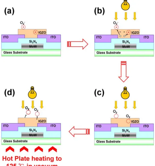
Figure 3. Schematic diagram of the oxygen removal processes by illuminating and heating treatment.
Here, we addressed a method to remove the remaining gas species adsorbing chemically, that the vacuum pump cannot evacuate. In this manner, the light, heat, and vacuum pump were employed simultaneously. In ZnO-based materials, the free electrons in the a-IGZO film tend to be trapped by physically adsorbed acceptors, which results in the chemisorbed oxygen in the a-IGZO film, as seen in figure 3 (a). Under the light illumination, figure 3 (b) shows the holes originated from the electron-hole pairs are
strongly drawn to the chemisorbed oxygen, causing a recombination of the hole and the negative charged oxygen. Hence, the oxygen adsorbing mode converted from the chemisorbed (O2-) to the physically adsorbed mode (O2) shown in figure 3 (c). At this
time, the adsorbing force was mainly the van der waal force and the oxygen adsorbed physically. The physically adsorbed oxygen would leave the a-IGZO film by obtaining the additional thermal energy, as shown in figure 3 (d) to overcome the van der waal force, which could drive out the water existing in a-IGZO film. Furthermore, the vacuum pump system must evacuate the adsorbing gas species immediately to prevent the re-adsorption. Hence, the adsorbing oxygen on a-IGZO film can be removed more clearly by the illuminating and heating treatment in an evacuating condition than only the vacuum pump was utilized.
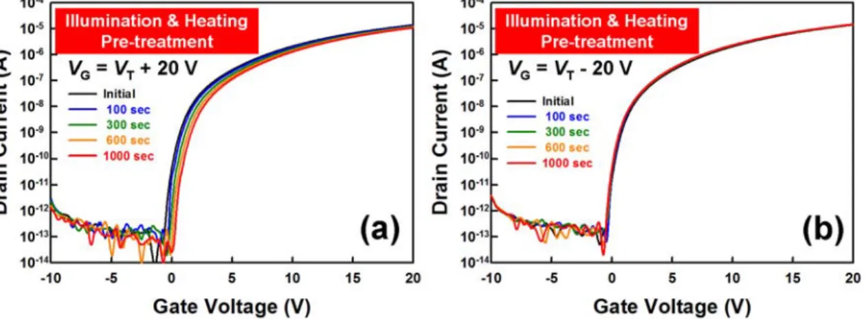
Figures 4 (a) and 4 (b) show the IDS-VG transfer characteristics curves of a-IGZO
TFTs with the illuminating and heating pre-treatments under the gate bias stress of 1000 sec in a vacuum environment. The device characteristics exhibited an improvement in figure 4 (a), where the positive gate bias-induced positive shift of threshold voltage reduced to 1.29 V. Figure 4 (b) shows the good stability and hump-free characteristics of
a-IGZO TFT. Accordingly, the illuminating and heating pre-treatments for removal the
adsorbing gas species of the a-IGZO TFTs are helpful to improve the device bias stability.
Figure 4. Time evolution of ID -VG transfer characteristics curves of a-IGZO TFTs with
illuminating and heating pre-treatment under (a) positive and (b) negative gate bias stress. In order to confirm whether the formation of hump is affected by the water or oxygen
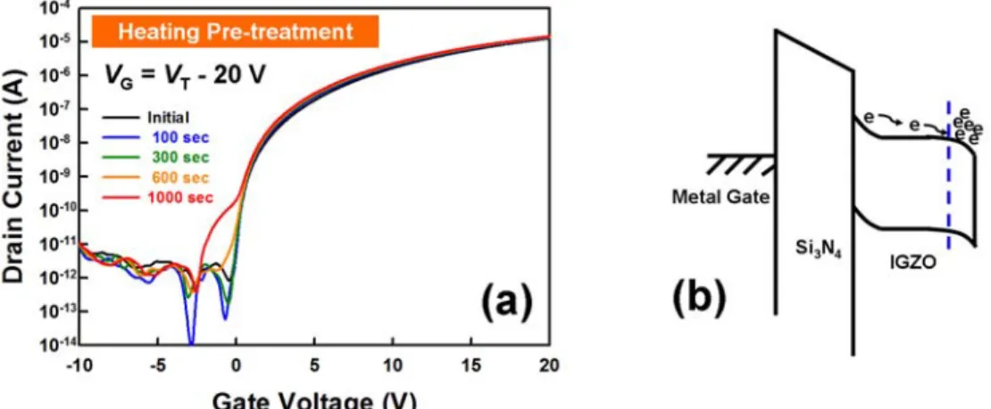
adsorption, the device with thermal pre-treatment at 125 ℃ for removal the adsorbing
water molecules was experienced a negative gate bias, and the experimental results were shown in Figure 5 (a). Clearly, a smaller hump in comparison with the hump appearing in the device without pre-treatment was observed at the stressing time of 1000 sec. Figure 5 (b) shows the energy-band diagram with water adsorbing on the a-IGZO film as the negative gate bias was conducted. As the negative gate bias was applied on the gate electrode, the energy-band of the a-IGZO near the gate electrode bent upward. And the absorbing water would lead to the energy-band bending downward due to the electron donation-induced Fermi-level raising. Then, the electrons in the a-IGZO film would accumulate at the back-channel of the a-IGZO TFTs generating a new channel, which would promote the formation of the hump. Accordingly, the water adsorbing on the a-IGZO film may result in the formation of new channel and cause the hump phenomenon as the stressing time was prolonged, due to the large amount of electrons accumulating at the back-channel.
Figure 5. Time evolution of ID -VG transfer characteristics curves of a-IGZO TFTs with
thermal pre-treatment under negative gate bias stress. (b) The energy-band diagram with water adsorbing on a-IGZO film as the negative gate bias was conducted, where the electrons accumulates at the back-channel.
Furthermore, the influence of the oxygen adsorption was examined by the same experiments, where the device was experienced the illuminating and heating pre-treatments to exclude the water effect and then the gate bias stresses were employed in the oxygen-rich environment. The experimental results are shown in figures 6 (a) and 6 (b). After positive gate bias stress, the transfer curve shift exhibited the same trend with previous results and the value of the threshold voltage shift was 4.16 V larger than the device without pre-treatment, which was mainly ascribed to the electric-field-induced oxygen adsorption on the a-IGZO surface. On the other hand, the threshold voltage shifted to the negative side to 1.00 V and there was no hump phenomenon appearing in the transfer curve. Therefore, the oxygen molecules influenced the threshold voltage value obviously while have no impact on the occurrence of hump phenomenon. Based on the above discussion, we can conclude that the hump phenomenon is ascribed to the additional channel at the surface induced by the water adsorption.
Figure 6. Time evolution of ID -VG transfer characteristics curves of a-IGZO TFTs with
oxygen gas pre-treatment under (a) positive and (b) negative gate bias stress.
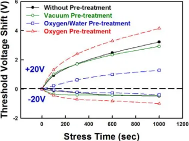
According to the aforementioned experimental results, the threshold voltage evolution under the positive/negative gate bias stress can be sketched in figure 7. Regardless of the positive or the negative gate bias stress, the a-IGZO TFTs with oxygen gas pre-treatment had the largest shifting value mainly due to the oxygen adsorption. On the contrary, the
device with the illuminating and heating pre-treatments owned the smallest value of threshold voltage shift because of the higher oxygen/water removal efficiency.
Figure 7. Variation in threshold voltage shift of a-IGZO TFT to which VT ± 20 V gate
bias stress was applied with various pre-treatment. Conclusion
In summary, the existence of oxygen/water in the surrounding environment affects the threshold voltage of sol-gel derived a-IGZO TFTs obviously. The a-IGZO TFT with the illuminating and heating pre-treatments under the positive/negative gate bias in vacuum ambient had the smallest threshold voltage shift as the stress duration increased. And the a-IGZO TFT with an oxygen gas pre-treatment exhibited an obvious variation due to the oxygen adsorption. Besides, the water adsorption on the a-IGZO surface, resulting in the energy band bending downward and further inducing the formation of new channel, caused a hump phenomenon under the negative gate bias. These electrical instabilities were contributed by the charge trapping of the gate insulator and the oxygen/water adsorption on the active layer of a-IGZO TFTs. The result also implies that the illuminating and heating pre-treatments for the a-IGZO film can improve the device stability by removal of water and oxygen adsorption. Furthermore, these results can be as important information for the subsequent passivation process concerning the pre-treatment of the active layer.
TABLE I. The threshold voltage evolution with the increasing positive-gate-bias-stress time of the a-IGZO TFTs with various pre-treatments.
Time
(sec) Without Pre-treatment Vacuum Pre-treatment Illumination and Heating Pre-treatment Oxygen Gas Pre-treatment
Initial 3.32 3.01 2.66 3.72 100 4.24 4.03 2.89 5.03 300 5.25 4.72 3.29 6.12 600 5.80 5.36 3.66 7.01 1000 6.55 5.94 3.94 7.87 Delta VT 3.23 2.93 1.29 4.16
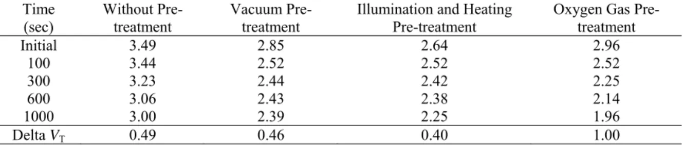
TABLE Ⅱ. The threshold voltage evolution with the increasing negative-gate-bias-stress time of the a-IGZO TFTs with various pre-treatments.
Time
(sec) Without Pre-treatment Vacuum Pre-treatment Illumination and Heating Pre-treatment Oxygen Gas Pre-treatment
Initial 3.49 2.85 2.64 2.96 100 3.44 2.52 2.52 2.52 300 3.23 2.44 2.42 2.25 600 3.06 2.43 2.38 2.14 1000 3.00 2.39 2.25 1.96 Delta VT 0.49 0.46 0.40 1.00 Acknowledgments
This work was performed at National Science Council Core Facilities Laboratory for Nano-Science and Nano-Technology in Kaohsiung-Pingtung area and was supported by the National Science Council of the Republic of China under Contract Nos.NSC-99-2120-M-110-001 and NSC 97-2112-M-110-009-MY3.
References
1. E. M. C. Fortunato, P. M. C. Barquinha, A. M. B. G. Pimentel, A. M. F. Gonçalves, A. J. S. Marques, R. F. P. Martins, and L. M. N. Pereira, Appl. Phys.
Lett., 85, 2541 (2004).
2. N. L. Dehuff, E. S. Kettenring, D. Hong, H. Q. Chiang, J. F. Wager, R. L. Hoffman, C. H. Park, and D. A. Keszler, J. Appl. Phys., 97, 064505 (2005).
3. K. Nomura, H. Ohta, A. Takagi, T. Kamiya, M. Hirano, and H. Hosono, Nature,
432, 488 (2004).
4. K. Nomura, H. Ohta, K. Ueda, T. Kamiya, M. Hirano, and H. Hosono, Science,
300, 1260 (2003).
5. G. H. Kim, B. D. Ahn, H. S. Shin, W. H. Jeong, H. J. Kim, H. J. Kim, Appl. Phys.
Lett., 94, 233501 (2009).
6. G. H. Kim, H. S. Shin, B. D. Ahn, K. H. Kim, W. J. Park, and H. J. Kim, J.
Electrochem. Soc., 156, H7 (2009).
7. G. H. Kim, H. S. Kim, H. S. Shin, B. D. Ahn, K. H. Kim, and H. J. Kim, Thin
Solid Films, 517,4007 (2009).
8. H. Q. Chiang, J. F. Wager, R. L. Hoffman, J. Jeong, and D. A. Keszler, Appl.
Phys. Lett., 86, 013503 (2005).
9. G. H. Kim, B. D. Ahn, H. S. Shin, W. H. Jeong, H. J. Kim, H. J. Kim, Appl. Phys.
Lett., 94, 233501 (2009).
10. M. K. Kim, J. H. Jeong, H. J. Lee, T. K. Ahn, H. S. Shin, J. S. Park, J. K. Jeong, Y. G. Mo, and H. D. Kim, Appl. Phys. Lett., 90, 212114 (2007).
11. D. H. Lee, Y. J. Chang, G. S. Herman, and C. H. Chang, Advance Material
(Weinheim, Ger.), 19, 843(2007).
12. G. H. Kim, H. S. Shin, B. D. Ahn, K. H. Kim, W. J. Park, and H. J. Kim, J.
Electrochem. Soc., 156, H7 (2009).
13. P. Barquinha, L. Pereira, G. Goncalves, R. Martins, and E. Fortunato, J.
Electrochem. Soc., 156, H161 (2009).
14. W. F. Chung, T. C. Chang, H. W. Li, C. W. Chen, Y. C. Chen, S. C. Chen, T. Y. Tseng, and Y. H. Tai, Electrochemical and Solid-State Letters, 14, H114 (2011).
15. W. F. Chung, T. C. Chang, H. W. Li, S. C. Chen, Y. C. Chen, T. Y. Tseng, and Y. H. Tai, Electrochemical and Solid-State Letters, 14, H235 (2011).
16. W. F. Chung, T. C. Chang, H. W. Li, S. C. Chen, Y. C. Chen, T. Y. Tseng, and Y. H. Tai, Appl. Phys. Lett., 98, 152109 (2011).
17. T. C. Chen, T. C. Chang, C. T. Tsai, T. Y. Hsieh, S. C. Chen, C. S. Lin, M. C. Hung, C. H. Tu, J. J. Chang, and P. L. Chen, Appl. Phys. Lett., 97, 112104 (2010). 18. Y. C. Chen, T. C. Chang, H. W. Li, S. C. Chen, J. Lu, W. F. Chung, Y. H. Tai, T.
Y. Tseng, Appl. Phys. Lett., 96, 262104 (2010).
19. E. N. Cho, J. H. Kang, C. E. Kim, P. Moon, and I. Yun, IEEE Trans. Device and
Materials Reliability, 11, 112 (2011).
20. D. Kang, H. Lim, C. Kim, I. Song, J. Park, and Y. Park, Appl. Phys. Lett., 90, 192101 (2007).