T
he analysis and modeling of human neural systems has long been a very important research field where many concepts can be applied to many applications in intelligent machines performing human-like speech, image, or other neural signal processing. The resultant tech-nological models have led to the development of new compu-tational methodologies and artificial neural networks (ANNs). It is always a great challenge to design neuro-morphic or n e u r o - i n s p i r e d A N N s t omimic both structures and functions of the brain as well as neural sensors such as the eyes, ears, nose, tongue, skin, etc. This is mainly due to complicated structures and dedicated functions of the brain and neural sensors. It is known that a human brain may consist of 1011 neurons with over 103
inter-connections per neuron. It performs dedicated functions in a highly parallel processing manner. In human eyes, the retina has millions of cells performing image sensing, smoothing, feature extraction, and dynamic processing.
By Chiu-Hung Cheng,
Chung-Yu Wu,
Bing Sheu, Li-Ju Lin,
Kuan-Hsun Huang,
Hsin-Chin Jiang,
Wen-Cheng Yen,
and Chiao-Wei Hsiao
Neuron-Bipolar Junction Transistor
(
νBJT) Circuits Enable the Formation
of Cellular Networks and Human
Neural Sensors Such as the Retina
Digital Stock 1996/ 1997 John Foxx
Increasing research ef-forts have focused on solv-ing the challenges of realizing that feasible ANNs should have a simple struc-ture suitable for microchip realization as well as mimic some specific neural func-tions. One of the successful
examples is the cellular neural network (CNN) proposed by Chua and Yang [1], which is a specific type of “analogic” nonlinear pro-cessor array. Due to its continuous-time dynamics and paral-lel-processing feature, the cellular network is very effective in real-time image processing applications such as noise removal, edge and corner detection, hole filling, connected component de-tection, and shadowing. Moreover, regularity, parallelism, and lo-cal connectivity in the cellular network architecture make it suitable for VLSI implementation.
Besides the structure simplification for practical realiza-tion, the basic components to realize cellular networks or neural sensors should consist of compact microelectronic de-vices or nanoelectronic dede-vices.
Thus, many neurons or cells can be implemented within a reasonable size to achieve the complex and dedi-cated neural functions. This means that fundamental device physics needs to be applied to realize neural behavior.
In this article, a novel device structure called the neuron-bipolar junction transistor (νBJT), for the c o m p a c t i m p l e m e n t a t i o n o f large-neighborhood cellular net-works and silicon retinal processing components is described. The basic device physics ofνBJTs is based on the carrier diffusion within the com-mon base region so that aνBJT in an array structure can be coupled to an-other without direct interconnec-tion. Through this mechanism, νBJTs can be used to form neuron cells in the cellular networks and large-neighborhood structures can be realized in a small chip area. Simi-larly, the base carrier diffusion mechanism of a νBJT array can be applied to the realization of the smoothing function of horizontal cells in the retina. Thus, a compact silicon retina can be designed for dif-ferent applications of real-time im-age processing.
Device Structure of
Neuron-Bipolar
Junction Transistors
The device structure of neuron-bipolar junction t r a n s i s t o r s (νBJT) is shown in Fig. 1(a) where the parasitic pnp BJT in N-well CMOS technology is used as an example. All the pnp BJTs have the same N-well base region and form an array. If the transistor Qjis turned on, the base carriers (i.e., electrons) can diffuse through the base spreading resistance RBto otherνBJTs so that they are turnedon. The amount of carriers diffusing to theνBJTs depends on the value of RBand the distance to the firedνBJT Qj. Similarly,
otherνBJTs can diffuse their base carriers to Qj. Once again, the amount of carriers reaching Qjdepends on RBand the
dis-tance. Equivalently, theνBJT Qjis a neuron that interconnects with other neurons to send its state output to them or receive multiple state inputs from them. The device symbol of aνBJT is shown in Fig. 1(b). P-Substrate RBj C N-Well Qj 1− N-Well B Ej+1 p+ n+ Ej+2 Ej Ej 1− RBj+1 RBj 1− Qj Qj+1 Qj+2 E B 1 B n C p+ p+ p+ p+ (a) (b)
1. (a) The cross-sectional view of the proposed neuron-bipolar junction transistor (νBJT).
(b) The symbol ofνBJT.
The three major functions of the retina
are photoinput sensing, edge extraction,
Since the spread emitter current of aνBJT transistor is determined by the carrier diffusion in the base, such current can be controlled by the base resistance value RB. A large RB
leads to small spread current and narrow spread range. A controllable RBcan be realized as the drain-source
resis-tance RDSof an NMOS device operated in the linear region as
shown in Fig. 2.
The HSPICE-simulated and model-calculated emitter cur-rents of 32νBJTs in a linear array of νBJTs are shown in Fig. 3 [2] where oneνBJT is turned on with 0.4-µA base current drive. It can be seen from Fig. 3 that otherνBJTs have smaller emitter currents caused by base carrier diffusion. The range of current distribution can be controlled by RDSthrough the gate voltage VG.
νBJT Smoothing Network
for a Silicon Retina
The retina is the early processing element in the visual nervous system of the vertebrate. It can perform three major functions in
image processing, and it sends out suitable signals to the brain. The three major functions are photoinput sensing, edge extrac-tion, and moving-object feature extraction.
In the outer-plexiform layer of the retina, there are three major cells, namely the photoreceptor, the horizontal cell, and the bipolar cell [3]. The major function of photoreceptors is to transduce light into electrical signals whereas that of horizontal cells is to provide a spatial and temporal smoothing for the signals from the photoreceptors. The bipolar cells process the signals from both photoreceptors and horizontal cells. It is believed that the outputs of bipolar cells are proportional to the difference between photoreceptor signals and horizontal-cell signals so that the im-age edge can be extracted. Since the smoothing function of hori-zontal cells is a local operation instead of a global one, edge details in both light and dark areas of high-contrast images can be sensed clearly.
In the retina, the edge of an object is detected by the contrast between the surface of the object and the background. The gen-eral principle of edge detection can be understood by using the conceptual curves in Fig. 4. In Fig. 4, the response of the photoreceptors has a high (low) current in the light (dark) area whereas the response of horizontal c e l l s i s t h e s m o o t h i n g o f t h e photoreceptor response. By perform-ing the subtraction operation between the two responses, an abrupt differ-ence from negative to positive at the edge can be obtained. By detecting the zero-crossing point, the edge of the image can be detected reliably [4].
One compact and efficient way to incorporate the advantages of the retina in image processing is to realize the retina di-rectly in a silicon microchip, called the silicon retina. Thus, the computation cost can be re-duced and the processing speed can be en-hanced. Moreover, high-performance real-time image processing could be achieved. TheνBJT can be applied to the compact re-alization of photoreceptors and horizontal cells in the retina. In the proposedνBJT sili-con retina architecture [2]-[4], the parasitic pnp BJTs in N-well CMOS technology with open bases are used as phototransistors to sense the light and generate photocurrents like the photoreceptors. TheνBJT array with all bases connected together through MOSFETs as adjustable resistors is used as the smoothing network, which mimics the smoothing function of horizontal cells. The structure of a two-dimensional (2-D)νBJT retina is shown in Fig. 5, where each basic cell consists of an isolated pnp phototransistor as Pixel Position −16 −14 −12 −10 −8 −6 −4 −2 0 2 4 6 8 10 12 14 16 0.0 0.2 0.4 0.6 0.8 1.0 1.2 1.4 V =3.8 V; RG DS=1.5 MDS Ω V =3.9 V;G RDS=491 KΩ V =4.0 V;G RDS=241 KΩ V =4.2 V;G RDS=140 KΩ SPICE Simulation Model Calculation MOS: W/L=3 m/6 mµ µ I (mA) E
3. The SPICE simulation and model calculation results on the emitter current characteristics
of the proposedνBJT linear array with 0.4 µm single-point stimulus under different FET gate
biases with single-point stimulus.
N-Well Ej Ej 1− Ej+1 VG N-Well p+ N-Well p+ N-Well p+ n+ n+ n+ n+ n+ n+ n+ P-Substrate
a photoreceptor and a smoothing pnp phototransistor as a hori-zontal cell. When the light is incident upon one cell, it is simulta-neously incident upon the two floating bases of both the smoothingνBJT and isolated photo-BJT. Thus, the electron-hole pairs are generated at and nearby the depletion region of the two base-collector junctions. Due to the electric field in the deletion region, the generated electrons are swept into the base region whereas the holes are swept into the collector. The excess elec-trons in the base region are diffused out through the MOS resistor array. The results of the carrier diffusion and distribution make the emitter currents of theνBJT array perform the smoothing function of the retina. The proposed νBJT
structure is compact and fully compatible with CMOS technology. Thus, it can be easily integrated with other integrated circuits to form a VLSI microsystem.
In many applications, input images often have wide-ranging variations of intensity or contrast. This requires an adjustable smooth-ing range. To achieve adjustable smoothsmooth-ing, the gate voltage of the enhancement-mode NMOS in the smoothing network of Fig. 5 can be controlled. When the gate voltage is high, the NMOS device is operated in the strong-in-version region and has a small drain-source resistance. On the other hand, when the gate voltage is low, the NMOS device is operated in the subthreshold region and the drain-source resistance is large. Therefore, the MOS device can provide a wide range of resistance values to achieve the wide-range adjustment of the smoothing range.
In the design of the focal-plane-array (FPA) of the proposedνBJT silicon retina,
compact row/column selection circuits are required to achieve a small pixel area. Figure 6(a) shows the basic cell structure of the FPA of aνBJT silicon retina. Both isolated and smoothing BJTs at each pixel have extra emitters directly connected to the row line. Two PMOS devices are connected in series with the active emitters of BJTs to serve as the row switches SW1 and SW2 con-trolled by the row line. Through the switches, the emitter cur-rents can be sent to smoothing and isolated column lines biased at VE. In each cell, four NMOSFETs are connected from the smoothing BJT to the four neighbors to form the proposed 2-D BJT smoothing network. Equivalently, each cell has two NMOSFETs as shown in Fig. 6. All the gates of NMOSFETs are connected to the common gate line with the adjustable voltage
VG.
When the row line is selected through the row decoder, its voltage is set at ground. The extra emitters act as collectors of
Photoreceptors
Bipolar Cells (Difference) Horizontal Cells
Response Current
4. The conceptual response currents versus pixel position in the retina.
VG VG VG VG VG VG VG VG V VG E VE VE IES IEI VEBP VEBQ + − + − IB hv hv hv Smoothing PNP Isolated PNP VP VQ
5. The equivalent circuit of the proposed 2-DνBJT silicon retina.
Smoothing PNP Isolated Column Line (Biased at V )E GND Selected VE Deselected Row Line Gate GND Smoothing Column Line (Biased at V )E Isolated PNP IES SW1 SW2 IEI hv hv NMOS_Y NMOS_X
pnp BJTs and SW1 and SW2 are closed. Thus, the two emitter currents IEIand IESof isolated and smoothing pnp BJTs at the
se-lected pixel can be sent to the isolated and smoothing column lines, respectively. When the row line is de-selected, its voltage is raised to the emitter voltage VE. In this case, SW1 and SW2 are
open and the normal emitters of pnp BJTs are disconnected from
the column lines and become floating. However, the extra emit-ters connected to the row selection line are connected to VE.
With all the de-selected emitters of BJTs connected to VE, the
BJTs in the smoothing network can be kept in the normal state so that the normal smoothing operation can be performed.
An experimental chip of the proposed BJT-based silicon ret-ina has been designed and fabricated in a 0.5-µm N-well dou-ble-poly, double-metal CMOS technology. Figure 7 shows the chip and basic cell photographs of the fabricated 64× 64 FPA of the BJT-based silicon retina. In the quiescent state without im-age inputs, the power dissipation of the sensor array in the sili-con retina is very small, being that of a 64× 64 open-base BJT. Thus the total quiescent power dissipation is determined by the peripheral circuit and is about 45 mW. In the illuminated state, the power dissipation of the sensor array is caused by the photocurrents of the BJTs and depends on the image light inten-sity. The typical total active power dissipation of the silicon ret-ina FPA in the illumret-inated state is about 48 mW to 75 mW.
To verify the tunable smoothing function of the proposed BJT smoothing network, a nonregular cross pattern with non-uniform light intensity is projected on the experimental 2-D chip with the gate bias VGof NMOSFETs tuned at different
val-ues. Figure 8(a) shows the measured output responses of the isolated BJTs as the photoreceptors in the fabricated silicon retina and Fig. 8(b) shows the measured output responses of the BJTs in the proposedνBJT smoothing network with VGat
7. The chip photograph of the fabricated 64× 64 FPA of the vBJT
silicon retina. ε 60 50 40 30 20 10 0.05 0 10 20 30 40 50 60 60 50 40 30 20 10 10 20 30 40 50 60 0.01 0.02 0.03 0 ε 60 50 40 30 20 10 10 20 30 40 50 60 −0.02 0 0.02 ε 60 50 40 30 20 10 10 20 30 40 50 60 −0.02 0 0.02 ε
Y Axis X Axis Y Axis X Axis
Y Axis X Axis Y Axis X Axis
(d) (c) (a)
(b)
V =3.6 VG V =3.6 VG
8. The measured output responses of (a) isolated BJT array; (b)νBJT smoothing network with VG= 3.6 V; (c) silicon retina with VG= 3.6 V; and (d)
3.6 V, respectively. These responses represent those of the hori-zontal cells in the retina. When VG is equal to 3.6 V, the
NMOSFETs are operated in the subthreshold region and the channel resistance is the largest. So the pattern has the small-est smooth area as shown in Fig. 8(b).
Figure 8(c) and (d) shows the measured output responses of the proposed BJT-based silicon retina with VG= 3.6 V and 4.8 V,
respectively, which represent the responses of the bipolar cells in the retina. Figure 9(a) and (b) shows the mathematically found zero-crossing positions of the outputs of the BJT-based silicon retina as shown in Fig. 8(c) and (d), respectively. The zero-crossing points of the measured output voltages of the BJT-based silicon retina can be used to identify the edges of ob-jects. As shown in Fig. 9, when the smooth area is smaller, the
smaller variation of light intensity can be identified. In other words, the smaller con-trast edges can be identified.
Figure 10(a) and (b) shows the measured output temporal responses of a single pixel in the fabricated FPA chip of the BJT-based sili-con retina under three incident flash-light spot patterns with nearly the same intensity but different spot diameters. It can be seen in Fig. 10(a) that the positive pulse is generated when the flash-light source is turned on. The pulse has higher peak for smaller flash spot. When the light is turned off, the measured output temporal responses of the fabricated silicon retina decays to the off state as shown in Fig. 10(b). The small negative pulse is not observed because the large off transition time of the flash-light source allows both isolated and smoothing BJT to be turned off simultaneously. The peaks in Fig. 10(b) are in-duced by the closing time of the mechanical shutter used in this measurement.
One of the most important applications of the silicon retina is the bionic retina implant system [6]. Patients who have diseases of the retina lose their vision. The purpose of the bionic retina implant system is to implant a silicon retina chip to replace, at least part of, the diseased retina so that the blind patient with ret-inal disease may restore vision. Basically, the developing archi-tecture is conceptually shown in Fig. 11 where a silicon retina chip is implanted into the eyeball. The light reflected by an ob-ject or from an additional light source is used to generate the power supply for the chip by using the on-chip photovoltaic de-10 20 30 40 50 60 60 50 40 30 20 10 10 20 30 40 50 60 60 50 40 30 20 10 Y Axis Y Axis X Axis X Axis (a) (b) V =3.6 VG V =4.8 VG
9. The mathematically found zero-crossing positions of the measured output responses of the
proposed BJT-based silicon retina as shown in: (a) silicon retina with VG= 3.6 V and (b) silicon
retina with VG= 4.8 V. 0 V 50 mv/div 205 mV −215 mV Large Medium Small Final State of Large Spot Final State of Medium Spot Final State of Small Spot 1 ms/div 0 V 205 mV −215 mV (a) 50 mv/div (b) Small Medium Large 0 V
10. The measured output (a) turn-on and (b) turn-off temporal responses of a single pixel in the improved 2-DνBJT silicon retina
vices. Thus, no external battery is required. Meanwhile, the reti-nal processing circuit is also integrated on the microchip to generate retinal pulses that are sent to ganglion cells. Through the ganglion cells, the pulses are sent to brain for vision. The sili-con retina implant system will be a great challenge in the bioelectronics area.
νBJT Applications on Large-Neighborhood CNNs
The general architectures of cellular networks with the numberr of connected neighborhood layers equal to 1 and 2 are shown in
Fig. 12(a) and (b), respectively. In Fig. 12(a), the central neuron cell only receives the four state outputs of the nearest four neighboring cells with unity weighting factor and its own state outputs with the weighting factor of 1. The values shown in the cells are coefficients of the A templates, which correlate one cell’s state input with other ones of neighboring cells. Only near-est neighboring cells interact with the cell. Thus, the number of
connected neighborhood layers is equal to 1. If the state outputs of the second layer of neighboring cells is also input to the cen-tral cell with template coefficients as shown in Fig. 12(b), we have r = 2. Such a cellular network is called the large-neighbor-hood cellular network. Generally, it is difficult to directly imple-ment the large-neighborhood cellular network because there are too many interconnections per cell. The resultant cell area would not be bearable.
To compactly implement cellular networks with single- and large-neighborhood templates [7],νBJTs are used as neurons with their base regions connected together through MOS resis-tors or some gain stages [8]. The base carrier diffusion mecha-nism is used for large-neighborhood connection. The base currents, which serve as state inputs or output currents, are de-creased through the control of MOS resistors and/or amplified through gain stages. In such architectures, symmetrical or asymmetrical templates can be realized by adjusting the gate voltages of MOS devices. The cellular networks realized byνBJTs are called theνBJT cellular networks. In a νBJT cellular net-work, the synapse values in the template can be adjusted through the gate voltages of MOS devices. The self-feedback function is compactly realized by incorporating a PMOS transis-tor with theνBJT. The resultant structure is similar to that of the lambda bipolar transistor [9] and has a small chip area. The neu-ron input can be applied to the base of aνBJT through the NMOS transistors. Due to the compact structure, theνBJT cellular net-work requires a small chip area and has high integration capabil-ity. Since the neurons are realized byνBJTs, which can also be served as the phototransistors, the optical images can be entered directly to theνBJT cellular network without adding any sepa-rate sensor device.
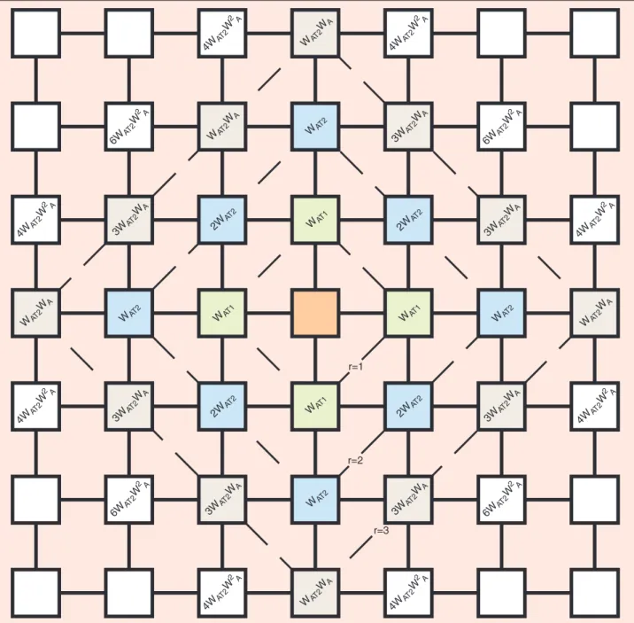
0 0 0 0 0 0 0 0 0 0 0 0 1 0 0 0 1 2 1 0 0 0 1 0 0 0 0 0 0 0 0 0 0.156 0 0 0 0 0 0 0 0.277 1.11 0.277 0 0.156 1.11 2 1.11 0.156 0 0.277 1.11 0.277 0 0 0 0.156 0 0 r=2 r=1 (a) (b) r=2 r=1
12. The A templates with the number r of connected neighborhood layers equal to (a) 1 and (b) 2. Implanted
Chip
Light Source Reflected
Light
νBJT CNN with Symmetrical Templates
The basic cell circuit of theνBJT cellular network with a symmetrical template is shown in Fig. 13, where the neuron is realized by theνBJT QBwith the NMOS transistor MN2biased by the gate voltageVBIASto generate the standby base current IBO=
IBIAS. Such a neuron is called theνBJT neuron. The neuron’s output current IEflows through the load
PMOS device MP3to generate the neuron output voltage VEC. The neuron state voltage is the base
voltage VB. For each IBIASvalue, the corresponding
VBvalue is unique. Thus, the current IBIAScan also
be used to realize the Z template [1], as will be de-scribed later.
In theνBJT neuron of Fig. 13, MP1provides a positive feedback to QBso that the negative resis-tance is generated and the neuron has two stable states. Thus, theνBJT cellular network is of the monotonic type of binary-valued cellular networks.
The self-feedback synapse of the A template in the cellular network is realized by the current IPof
the positive-feedback PMOS transistor MP1with its gate connected to the ground and source (drain) connected to the emitter (base) of QB. The structure of QBand MP1is called the lambda bipolar transistor as reported in [9]. In realizing the lambda bipolar
transistor, MP1can be compactly implemented in the N-well base region with its source shared with the emitter of QBand its N-well substrate shared with the base of QB. Thus, the substrate of MP1is connected to its drain and the positive substrate bias ex-ists [9]. Since the neuron structure combines νBJT with the lambda bipolar transistor, it can be called the neu-ron-lambda-BJT neuron orνλBJT neuron. As shown in Fig. 13, the input capacitance of theνλBJT neuron is the capacitance seen at the base node, which is dominated by the base-emitter junction capacitance. The input resistance is the resistance seen at the base node, which is the input resistance of QBin parallel with the output resistance of MP1.
The synaptic coefficients of the A template can be realized by adjusting the self-feedback current IPand the four output
cur-rents IOU, IOD, IOR, and IOLto the four neighboring cells. This can
be achieved by controlling the resistance of NMOS transistors in Fig. 13 through their gate voltages. The synaptic coefficients of the B template can be represented by the current IINto the mas-ter neuron and the currents INNito the neighboring neurons as
shown in Fig. 13, which can be adjusted by the corresponding gate voltages. In this way, the synaptic coefficients of the B tem-plate must have positive sign.
By using the circuit of theνλBJT neuron as shown in Fig. 13, a 2-DνBJT cellular network can be formed. The fixed (Dirichlet) boundary condition is used to theνBJT cellular network. To ver-ify its function, three applications with symmetrical templates are tested in theνBJT cellular network by using the HSPICE cir-cuit simulation.
In the noise-removal operation, the cloning template is listed in Table 1 where the central weight is two times larger than its four neighboring weights [1]. To implement the noise removal operation, first the suitable gate voltages are applied to the gate of the MOS transistors realizing the template coefficients. Then the initial image pattern is applied to the input base node of the neuron as the initial condition. Secondly, the initial input is taken away by turning off MINIin Fig. 13, and theνBJT cellular network starts its operation. After the transient time, theνBJT cellular network can reach a steady state. The transient time de-pends on the resistance and the capacitance in theνλBJT neu-ron. The final steady state can be read out by sending out the state voltage VB. Figure 14(a) shows the initial noisy image used
to test the noise removal capability of the proposedνBJT cellular network. The image size is 32× 32 pixels and the νBJT cellular network has 32× 32 cells. The HSPICE-simulated output image
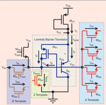
MND IOU MNU MNR MNL IOD IOR IOL VBIAS QB IE MN2 MP1 VEC IP IB ISUM + VEC − + VEB − Lambda Bipolar Transistor
VDD MP3 IS MINI VINI VGINI VGIN VIN A Template Z Template B Template VB MNI MNNi INNi IIN I BIAS
13. The complete cell circuit of oneνλBJT neuron in the νBJT CNN.
Table 1. Symmetrical CNN Templates
Application A B Z Noise removal CNN 0 1 0 1 2 1 0 1 0 0 0 0 0 0 0 0 0 0 0 Erosion CNN 0 0 0 0 2 0 0 0 0 0 1 0 1 1 1 0 1 0 −4.5
from theνBJT cellular network is shown in Fig. 14(b). It can be seen from Fig. 14(b) that the noise has been eliminated.
As a second example, the erosion operation is tested. The ero-sion templates are listed in Table 1 [7]. To implement the B tem-plate, the NMOS transistors MNIand MNNifor i = 4 as shown in Fig. 13 should be used. Figure 15(a) shows the input image used to test the image erosion operation. The HSPICE-simulated out-put image from theνBJT cellular network is shown in Fig. 15(b), which verifies the correct function of theνBJT cellular network in the erosion operation.
Smaller coupling resistors between neurons lead to a slower decreasing rate of the currents sending from one neuron to other neurons. Thus the farther neurons can receive the current from the master neuron through its neighboring neuron without extra interconnection. Based upon the above principle, the coupling re-sistor can be used to control the connected layers of neighboring neurons in the cellular network. Figure 12 shows the A templates for the noise removal image processing with the number of neigh-borhood layers r = 1 and r = 2, respectively. In the r = 2 template,
the synaptic coefficients decrease with the distance from the cen-tral coefficient. In the template with r = 2, the synaptic coefficients are determined from the output current of a neuron in the high stable state (white) to the first-neighborhood neuron in the tran-sition point from low to high stable state and to the second-neigh-borhood neuron in the low stable state (black).
By using the A template with r = 1 as shown in Fig. 12(a) and the input noisy image of Fig. 14(a) in theνBJT CNN, the output image is shown in Fig. 14(b) where the four-pixel square black or white noise images are not removed even if the self-feedback co-efficient is reduced from 2 to 1. However, these noise images can be removed by using the A template with r = 2 as shown in Fig. 12(b). Since in the A template with r = 2 there is a larger spatial mask of 5× 5, they have stronger local averaging effects that make all the white (black) noisy pixels in the local region change to the black (white) ones when the total number of black (white) pixels is larger than that of white (black) pixels. From the above simulation results, it can be seen that the noise removal capabil-ity is enhanced for r > 1.
νBJT CNN with
Asym-metrical Templates
To realize the asymmetrical template coefficients with posi-tive or negaposi-tive signs, a new synapse structure for theνBJT cellular network is proposed as shown in Fig. 16. In Fig. 16, the simple coupling MOS devices among the basic cell are re-placed by the fully programma-ble weight stages PWA, PWB, and PWB0. The PWAstages real-ize the A template whereas the PWB and PWB0 stages realize the B template.The A template is realized by the stages PWA, PWA1, and PWA2. The neuron output cur-rent is sent to the neighboring neurons through the stage
(a) (b)
14. (a) The initial image and (b) the final output image in theνBJT
CNN under the noise removal operation.
(a) (b)
15. (a) The input image and (b) the output image in theνBJT CNN
under the image erosion operation.
VGN IE(n) VBIAS VINI(n) VINI QB(n) MP3 MN2 MP1 IOUT VB(n) VDD to C(m 1,n) cell− to C(m+1,n) cell to C(m,n 1) cell− to C(m,n+1) cell QB3(n) A Template Vin(m,n) PWB B Template PWA PWA PWA PWA ID IB VEB VEC + + − − VC VSEL( )− VSEL(+) IIN QB2(n) MN6 MN7 MN5 PWB PWB PWB I BI AS PW B0 I BQ CQI BQI CQI
PWA2 that performs the current-to-current con-version with a suitable pos-itive gain.
Each of the fully pro-grammable weight stages PWA, PWB, and PWB0 in Fig. 16 has the same circuit structure. It consists of one MOS transistor MN5 with the gate voltage VGNas the
adjustable coupling resis-tor; two MOS transistors
MN6and MN7as switches controlled by VSEL(+)and VSEL(−), re-spectively; and two common-emitter amplifiers with PNP lateral BJTs QB2and QB3; collector bias current source ICQ; and base
bias current source IBQ. The absolute value of the weight can be
adjusted through the gate voltage VGNof the coupling MOS
re-sistor MN5. To realize the sign of the weights, the control volt-ages VSEL(-)and VSEL(+)are used to turn on MN7for negative weights and MN6for positive weights. Therefore, two control sig-nals are needed for each weight. If the input current IINis zero, both QB2and QB3are in the active region with IBQ= IBIand ICQ=
βLIBQ=βLIBIso that the output current IOUTis zero. If the input
current IINapplied to the base of QB2is positive (negative) and VSEL(+)is 3 V, IOUTdenoted as IO(+) is positive (negative) as a
souring (sinking) current flowing out of (into) QB3. On the other hand, if IINis positive (negative) and VSEL(-)is 3 V, IOUTdenoted as IO(−) is negative (positive) as a sinking (souring) current
flow-ing into (out of) QB3. In the circuit shown in Fig. 16, the parame-ters are set as VDD= 3 V, Vc= 1.15 V, IBQ2= IBQ3= 0.3µA, and ICQ2
= ICQ3= 20µA. The current gain βLis 60.5.
By using the above-mentioned circuitry, a large-neighbor-hood cellular network can be realized. Given the template coeffi-cients WATrof the rth neighborhood layer, WA, WA1, and WA2of
the stages PWA, PWA1, and PWA2can be determined, respectively. Similar to the A template, the B template can be realized by WB, WB0, WB1,
and WB2of the stages PWB, PWB0,
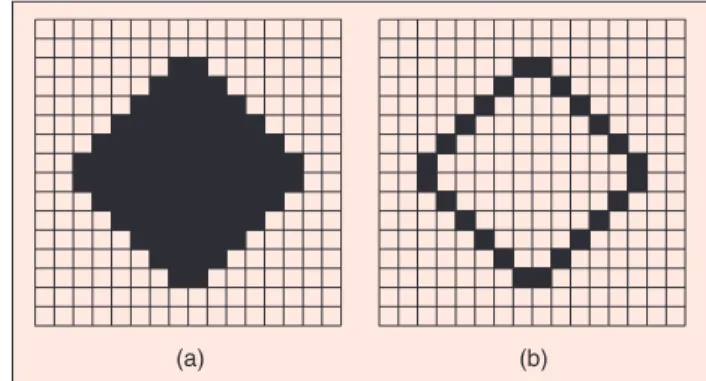
PWB1, and PWB2, respectively. Two image-processing func-tions are applied to the test of the νBJT cellular network with an asymmetrical single-neighbor-hood template. First, Fig. 17(a) shows the input image of a filled di-amond pattern used in the edge-de-tection operation of the proposed fully programmableνBJT cellular network with a single neighbor-hood. The size of theνBJT cellular n e t w o r k i s 1 6 × 16. The HSPICE-simulated output image is shown in Fig. 17(b). It can be seen
from Fig. 17(b) that the edge of the diamond pat-tern has been extracted. S e c o n d l y , t o t e s t t h e shadow-projection opera-tion, both A and B tem-plates [9] in Table 2 are used. To realize the B tem-plate, the input image
Vin(m,n)is sent to theνBJT cells through the PWB0 stage and the neighboring cells through the PWB stage. Both the PWB0and PWBstages are the same as the PWA stage. The gate voltage VGINis adjusted to make IOUTto be the
same as the self-feedback current IPin the A template. Each
boundary cell is in the fixed condition. The neuron states are all initialized to the black stable state.
The proposed general structure of theνBJT cellular network with a large neighborhood is shown in Fig. 18, where the pro-grammable weights of A and B templates are realized by the fully programmable stages that have the same structure as shown in
(a) (b)
17. (a) The input image to the proposedνBJT CNN for edge detection;
(b) the final output state of theνBJT CNN.
The proposed νBJT structure
is compact and fully compatible
with CMOS technology.
Thus, it can be easily integrated
with other integrated circuits to
form a VLSI microsystem.
Table 2. Asymmetrical CNN Templates
Application A B Z Edge Detection CNN 0 0 25 0 0 25 2 0 25 0 0 25 0 − − − − . . . . 0 0 0 0 0 0 0 0 0 −1 Corner Detection CNN 0 0 0 0 2 0 0 0 0 − − − − − − − − 1 1 1 1 8 1 1 1 1 −8.5 Muller-Lyer Arrowhead Illusion CNN 0 0 0 0 0 0 0 0 0 0 0 0 1 3 0 0 0 0 0 0 0 0 0 0 0 0 . − − − − − − − − − − − − 0 1 0 1 0 1 0 1 0 1 0 1 0 1 0 1 0 1 0 1 0 1 0 1 1 . . . . . . . . . . . . .3 0 1 0 1 0 1 0 1 0 1 0 1 0 1 0 1 0 1 0 1 0 1 0 1 − − − − − − − − − − − − . . . . . . . . . . . . −2.8
B Template PWB PWB PWB PWB PWB PWB PWA PWA PWA PWA PWA PWA PW B1 PW B2 PW B0 PW A1 PW A2 PW B1 PW B2 PW B1 PW B2 PW B0 PW B0 PW A1 PW A2 PW A1 PW A2 Vi n (m1 ,n ) − Vi n(m, n) Vi n(m+ 1,n) VB VFB IE VB VFB IE IE VB VFB A Template PWA PWA1 PWB PWB0 PWB2 PWA2 PWB1 IIN VSEL( )− QB3(n) QB2(n) MN7 MN6 MN5 VGN VSEL(+) I BQ CQI VC IOUT I BQ CQI VC MN5 Q B2(n) QB3(n) VGN I BQ CQI CQI Programmable Weight
Fig. 16. The fully programmable stage in Fig. 16 is used to realize the stages PWA, PWA1, PWB0, PWB, and PWB1as repeatedly shown in Fig. 18. The positive programmable stage without sign-selection MOS switches is used to realize the stages PWA2 and PWB1, as shown in Fig. 18.
To verify the correct functions of the proposed BJT cellular network structure with a large neighborhood, two examples are realized and simulated in an HSPICE circuit simulator. Each boundary cell is in the fixed condition. The first example is for the corner-detection operation. Both the A and B templates are listed in Table 2 [7], where the A template has only one self-feed-back weight. As compared with the template information shown in Fig. 19, the B template in Table 2 has two neighborhood layers with the negative weight WBT1=−1 and WBT2=−1 or 0. The
posi-tive central weight is eight times larger than those of the eight negative neighboring weights [7]. From Table 2, WB = 1,
WB1,WB2=−1, and WB0= 9.5.
Figure 20(a) shows the input image used to test the image cor-ner-detection operation. The HSPICE-simulated output image from theνBJT cellular network is shown in Fig. 20(b), which veri-fies the correct function of theνBJT cellular network in the cor-ner-detection operation. It should be noted that although the realized coefficients in the B template have some difference as compared with those in Table 2, the corner-detection function is still correct. Thus the difference is tolerable.
The second example is theνBJT cellular network for the Mul-ler-Lyer arrowhead-illusion function. Figure 21(a) shows the 32 × 32 input image used to test the Muller-Lyer arrowhead illusion
W W AT2 A 4W W AT2 2 A 4W W AT2 2 A 6W W AT2 2 A 3W W AT2 A WAT 2 WAT 1 WAT 1 W W AT2 A WAT 2 3W W AT2 A 6W W AT2 2 A 4W W AT2 2 A 4W W AT2 2 A 3W W AT2 A 3W W AT2 A 2W AT2 2W AT2 WAT 1 WAT 1 WAT 2 WAT 2 W W AT2 A W W AT2 A 2W AT2 2W AT2 3W W AT2 A 6W W AT2 2 A W W AT2 A 3W W AT2 A 6W W AT2 2 A 3W W AT2 A 4W W AT2 2 A 4W W AT2 2 A 4W W AT2 2 A 4W W AT2 2 A r=3 r=2 r=1
function of the realizedνBJT cellular network. In Fig. 21(a), there are two horizontal lines. One has diverging arrowheads at the ends whereas the other has converging arrowheads. Though the two lines are of the same length, the line with the converging arrowheads appears decidedly shorter. The HSPICE-simulated output image is shown in Fig. 21(b). It can be seen from Fig. 21(b) that the horizontal line with converging arrowheads be-comes shorter as expected. It should be noted that although the realized coefficients in the B template have some difference as compared with those in Table 2, the Muller-Lyer arrowhead-illu-sion function is still correct. Thus the difference is tolerable.
Conclusions
In this article, a new device structure called theνBJT was pre-sented. It has been successfully applied to the design of a silicon retina and large-neighborhood CNNs. TheνBJT-based smooth-ing array for the silicon retina has a simple and compact struc-ture, which is suitable for the VLSI implementation. It can be integrated with other CMOS retinal signal processing circuits to form smart sensor systems. On the other hand, based upon the νBJT structure, new compact νBJT CNN structures with pro-grammable large neighborhood templates for image processing have also been successfully designed in CMOS technology. The proposedνBJT CNN is designed to implement large neighbor-hoods without adding too many extra interconnections and cir-cuits. Using the proposed structure, the template coefficients with two neighborhood layers are fully realizable.
In the future, the research on efficient physical structures for the implementation of the bionic silicon retina functions or smart retinal processing will progress extensively toward nanoscale devices or integration. Further research on large-neighborhoodνBJT CNNs will also advance toward the nanoelectronics regime with the feasible development of a pow-erful nanoscale CNN universal machine(CNNUM).
Chiu-Hung Cheng is a Ph.D. student at National Chiao Tung
University in Hsinchu, Taiwan. Dr. Chung-Yu Wu is a Chaired
Professor at National Chiao Tung University and also serves as Founding Chair of Technical Committee on Nanoelectronics and Giga-Scale Systems for the IEEE Circuits and Systems Soci-ety. Dr. Bing Sheu is with Nassda Corporation and is 2001 Past President of the IEEE Circuits and Systems Society. Li-Ju Lin and Kuan-Hsun Huang are Ph.D. students and Chiao-Wei Hsiao is an M.S. student with the Integrated Circuits and Systems Lab at National Chiao Tung University. Hsin-Chin Jiang is the sec-tion manager of the Analog IP Technology Secsec-tion in the IP Technology Department of U2000/SoC Technology Center (STC) at the Industrial Technology Research Institute (ITRI) in Taiwan. Wen-Cheng Yen is an engineer at Terax Communica-tion Technologies Inc. in Hsinchu, Taiwan.
References
1. L.O. Chua and L. Yang, “Cellular neural networks: Theory,” IEEE Trans. Circuits Sys., vol. 35, pp. 1257-1272, Oct. 1988.
2. C.Y. Wu and H.C. Jiang, “An improved BJT-based silicon retina with tunable image smoothing capability,” IEEE Trans. VLSI, vol. 7, no. 2, pp. 241-248, Jun. 1999.
3. C.A. Mead, Analog VLSI Implementations of Neural Systems. Reading, MA: Addison Wesley, pp. 239-246, 1989.
4. A Hummel, “Representations based on zero-crossings in scale-space,” in Proc. IEEE Computer Vision and Pattern Recognition Conf., pp. 204-209, Jun. 1986.
5. C.Y. Wu and C.F. Chiu, “A new structure of 2-D silicon retina,” IEEE J. Solid-State Circuits, vol. 30, no. 8, pp. 890-897, Aug. 1995.
6. M. Schwarz, R. Hauschild, B.J. Hosticka, J. Huppertz, T. Kneip, S. Kolnsberg, L. Ewe, and T. Hoc Khiem, “Single-chip CMOS image sensors for a retina implant system,” IEEE Trans Circuits Syst. II, vol. 46, no. 7, pp. 870-877, Jul. 1999.
7. L.O. Chua, CNN: A Paradigm for Complexity (World Scientific Series on Nonlinear Science, vol. 31). Singapore: World Scientific, 1998.
8. C.Y. Wu and W.C. Yen, “A new compact neuron-bipolar junction transistor (νBJT) cellular neural network (CNN) structure with programmable large neighborhood symmetric templates for image processing,” IEEE Trans. Circuits Syst. I, vol. 48, no. 1, pp. 12-27, Jan. 2001.
9. C.Y. Wu “An analysis and the fabrication technology of the LAMBDA bipolar transistor,” IEEE Trans. Electron Devices, vol. ED-27, pp. 414-419, Feb.
1980. CD■
(a) (b)
20. (a) The input image and (b) the final output image in theνBJT
CNN under the corner detection operation.
(a) (b)
21. (a) The input image and (b) the HSPICE simulated final output