國
立 交 通 大 學
電子物理研究所
博士論文
在矽基板上成長三族氮化物
之磊晶及物性研究
Growth and physical properties of group
III-nitrides on Si substrates
研 究 生:辜瑞泰
指導教授:周武清 博士
在矽基板上成長三族氮化物之磊晶及物性研究
Growth and physical properties of group
III-nitrides on Si substrates
研 究 生:辜瑞泰 Student :Jui-Tai Ku
指導教授:周武清 博士 Advisor:Dr. Wu-Ching Chou
國 立 交 通 大 學
電子物理研究所
博 士 論 文
A Thesis
Submitted to Institute of Electrophysics
College of Science
National Chiao Tung University
in partial Fulfillment of the Requirements
for the Degree of
Doctor of Philosophy
in
Electrophysics
November 2011
Hsinchu, Taiwan, Republic of China
在矽基板上成長三族氮化物之磊晶及物性研究
研究生:辜瑞泰
指導教授:周武清博士
國立交通大學電子物理研究所
摘要
本論文利用分子束磊晶法在矽基板上成長氮化鎵、氮化銦奈米柱與銦極性及 氮極性的氮化銦薄膜。利用X光繞射、光激螢光光譜及拉曼光譜等實驗來研究其 物理特性。 於利用成長的溫度和氮/鎵(銦)比例控制氮化鎵(銦)奈米柱的高寬比。發現 在高度氮富含的條件下,氮化鎵(銦)奈米柱有較大的高寬比。以X光繞射與拉曼 光譜的量測證明每一奈米柱皆為無應力之單晶結構。再利用氮化鎵奈米柱為緩衝 層在矽基板上成長氮化鎵薄膜。發現當氮化鎵奈米柱的直徑小於80奈米時可成長 出無應力的氮化鎵薄膜。另一方面也利用氮化銦奈米柱為緩衝層在矽基板上成長 氮化銦薄膜,但因氮化銦奈米柱與矽基板間較弱的附著力,使氮化銦薄膜與矽基 板產生剝離的現象。而從低溫光激螢光光譜的量測結果發現,相較於氮化銦薄膜 成長在氮化鋁緩衝層上,其發光位置可由0.83電子伏特紅移至0.75電子伏特,螢 光光譜的半高寬值可由150毫電子伏特降為110毫電子伏特。結果證明相較於氮化 鋁緩衝層,在矽基板上以氮化銦奈米柱為緩衝層能有效改善氮化銦薄膜的品質。 此外,也利用改變氮化鋁緩衝層與矽基板間鋁原子層的厚度,成功地控制氮化銦 薄膜的極性。當鋁預沉積原子層的厚度大於一個原子層時,氮化銦薄膜的極性由 氮極性轉為銦極性。利用化學溶液蝕刻法來判斷氮化銦薄膜的極性,經過化學溶 液蝕刻後,氮極性的氮化銦薄膜表面變得粗糙且出現金字塔型的結構,銦極性的 氮化銦薄膜表面不受影響。Growth and physical properties of group
III-nitrides on Si substrates
Student:Jui-Tai Ku Advisors:Dr. Wu-Ching Chou
Institute of Electrophysics
National Chiao Tung University
ABSTRACT
In this dissertation, the growth of GaN nano-rods, InN nano-rods, In-polar and N-polar InN films on Si(111) substrate by molecular beam epitaxy (MBE) were studied. The x-ray diffraction (XRD), photoluminescence (PL) and Raman scattering were used to investigate the physical properties.
The morphology of GaN (InN) nano-rods can be manipulated by the control of N/Ga (In) ratio and growth temperature. From slightly N-rich condition to highly N-rich condition, the aspect ratio of III-nitride nano-rods increases. The results of XRD and Raman scattering measurements, show that III-nitride nano-rods were strain-free single crystals. Using GaN nano-rods as buffer layer, strain-free GaN film on Si substrate is realized. It is clearly demonstrated that the critical diameter of GaN
film overgrowth on InN nano-rods, film delimitation and cracking occurs during growth was observed. It is due to the poor adhesion between the rod and the Si substrate. Compare to the InN film grown on AlN/Si(111) substrate, low-temperature PL measurement shows that the emission peak energy of InN red shifts from 0.83 eV to 0.75 eV, and the full width at half maximum (FWHM) reduces from 150 meV to 110 meV. It implies that the InN film quality has been greatly improved. In addition, the lattice polarity of InN can be controlled by the thickness of initial Al-layer that was deposited prior to AlN buffer layer. A change from N-polar to In-polar was observed when Al-layer exceeded one monolayer. The lattice polarity of InN was determined by chemical wet etching method. In the case of N-polar InN, the surface became rough and pyramids after etching. In contrast, In-polar InN remained smooth surface.
誌謝(Acknowledgements)
隨著博士論文的完成也代表著漫長的求學生涯到此終告一段落。感恩老天在 最後的這段日子裡給予我的磨練,讓我體悟到自己的無知與渺小讓我學會了感恩 與懺悔。 能夠順利的完成這篇論文最要感恩我的指導教授周武清教授。感恩老師在博 士班期間對我的教導,尤其是最後的兩個月對我無私的付出及如親子般的教誨, 讓我在學術研究及處事態度都獲益良多。感恩老師在我論文迷惘的時候,幫我導 航給我明燈,讓我不會迷失因為有老師的耐心與愛心此篇論文才能夠順利的完 成。 感恩陳衛國教授、林烜輝教授、張文豪教授、謝振豪教授、楊祝壽教授、柯 文政教授,撥冗擔任博士口試委員,並且提供了許多寶貴的意見。感恩大同大學 楊祝壽教授以及高雄大學謝振豪教授從碩士班就一路的教導我,幫助我解決在分 子束磊晶與光譜上的種種問題,沒有您們我無法順利完成論文,感恩您們。感恩 楊宗熺博士。感恩您待我如親弟,總是不厭其煩的教導我無論是研究或是待人處 事都讓我獲益良多,從碩士班開始到博士班畢業都一直受您的照顧,感恩您。 感恩佛教如來宗 妙禪師父,感恩您讓我了悟人生真實義知道此生為何而來, 我會全力以赴依教奉行,永不放棄。感恩這一路上給予我幫助的所有人,沒有大 家的付出與護持瑞泰今日無法完成博士論文,感恩大家。 最後要感謝我的家人,不管是有形的資助還是無形的支持,沒有你們,這篇 論文無法順利的完成,最後要將這篇論文獻給在天上的爸爸,我拿到我們家族的 第一個博士了。Contents
Abstract (Chinese) I
Abstract (English) II
Acknowledgements IV Contents V
Table captions VII
Figure captions VIII
Chapter 1 Introduction 1
Chapter 2 Experimental details 7
2.1 Molecular Beam Epitaxy (MBE) system 7
2.2 X-ray diffraction 8
2.3 Photoluminescence 9
2.4 Micro-Raman scattering spectroscopy 10
Chapter 3 Overgrowth of GaN thin film on GaN nano-rods 18
3.1 Growth of GaN nano-rods 18
3.1.1 Growth procedure of GaN nano-rods 18 3.1.2 Influence of growth parameters on GaN nano-rods 19
3.1.3 X-ray analysis 22
3.1.4 Raman measurement 22
3.1.5 Conclusions of GaN nano-rods 23
3.2 GaN thin film overgrowth on GaN nano-rods 23 3.2.1 Growth procedure of GaN thin film 23
3.2.2 Structural properties 24
3.2.3 Optical properties 25
3.2.4 X-ray analysis 28
Chapter 4 Overgrowth of InN thin film on InN nano-rods 42
4.1 Growth of InN nano-rods 42
4.1.1 Growth procedure of InN nano-rods 42 4.1.2 Influence of growth parameters on InN nano-rods 43
4.1.3 X-ray analysis 45
4.2 InN thin film overgrowth on InN nano-rods 46 4.2.1 Growth procedure of InN thin film 46
4.2.2 Optical properties 46
4.3 Conclusions 47
Chapter 5 Polarity control of InN thin film grown on Si(111)
substrate
56
5.1 Growth procedure 56
5.2 Results and Discussion 57
5.3 Conclusions 60
Chapter 6 Conclusion 67
References 69
Tables captions
Table 3-1 The growth conditions of GaN nano-rods. 30 Table 4-1 The growth conditions of InN nano-rods. 48
Figure captions
Fig. 1-1 Atomic arrangement of two kinds of lattice polarities of III-nitrides: (a) cation ( Al, Ga, In )-polarity and (b) anion ( N )-polarity.
5
Fig. 1-2 A cross-sectional SEM image of overgrown GaN on NCs. 6 Fig. 2-1 The picture of major components of the ULVAC radio-frequency
plasma-assisted molecular beam epitaxy system.
11
Fig. 2-2 The partial pressure versus temperature of three different species (Al, Ga and In) effused by Knudsen-Cells.
12
Fig. 2-3 Optical emission spectrum of N2 plasma with incident power 250W
and N2-flow rate is 0.7 sccm.
13
Fig. 2-4 Atomic nitrogen emission intensity at 745 nm as functions of the N2-flow rate and the chamber pressure (top axis).
14
Fig. 2-5 Experimental setup for the GaN PL measurements. 15 Fig. 2-6 Experimental setup for the InN PL measurements. 16 Fig. 2-7 Schematic diagram of micro-Ranan system. 17 Fig. 3-1 Evolution of RHEED patterns for the growth process of vertically
aligned GaN nano-rods grown on Si(111) substrate. (a) and (b) are clean Si(111) - ( 7 × 7 ) reconstruction surface after thermal desorption. (c) and (d) are RHEED patterns of GaN nano-rods after the growth. The incident electron beam directions are along Si[11-2] (∥GaN [-1100] ) and Si[-110] (∥GaN [11-20]) directions, respectively. (e) is a schematic diagram of the crystal axes of GaN(0001) on Si(111).
31
Fig. 3-2 SEM images in the tilted (left) and plan (right) views of the vertically aligned GaN nano-rods grown on Si(111) at the same V/III ratio with growth temperature at (a) 800oC, (b) 830oC, and (c) 860oC,
Fig. 3-3 RHEED patterns of GaN nano-rods with growth temperature at (a) 800oC, (b) 830oC, and (c) 860oC, respectively. The incident electron
beam directions are along the [-1100] azimuth (left pattern) and [11-20] azimuth (right pattern).
33
Fig. 3-4 SEM images in the tilted (left) and plan (right) views of the vertically aligned GaN nano-rods grown on Si(111) at growth temperature 830oC with BEP of (a) Ga= 2.0×10⁻⁷ torr, (b) Ga= 7.1×10⁻⁸ torr and (c) Ga = 2.8×10⁻⁸ torr, respectively. The scale bar represents 1μm.
34
Fig. 3-5 X-ray θ-2θ scans of GaN nano-rods with different growth parameters. 35 Fig. 3-6 Raman spectra for GaN nano-rods grown with different growth
parameters.
36
Fig. 3-7 SEM images in the cross-sectional ( left ) and top ( right ) view of the overgrowth sample. The diameters of samples are (a) 60nm, (b) 80 nm and (c) 90 nm, respectively. The scale bars are 1 μm.
37
Fig. 3-8 Low-temperature (10 K) normalized PL spectra of three samples. 38 Fig. 3-9 Temperature-dependent PL spectra of three samples at temperature
range from 10 to 120 K.
39
Fig. 3-10 Room-temperature normalized Raman scattering spectra of three samples.
40
Fig. 3-11 X-ray 2θ-scans of the symmetric (0002) diffraction for three samples. 41 Fig. 4-1 RHEED patterns for the growth process of InN nano-rods on Si(111):
(a) Si(111)−(7×7) reconstruction surface; (b) After 30 sec InN nano-rods growth reconstruction surface; (c) After 30 min InN nano-rods growth; (d) The ending of InN nano-rods growth.
49
Fig. 4-2 SEM images in the top ( left ) and cross-sectional ( right ) view of the InN nano-rods grown on Si(111) at growth temperature 480oC with
BEP of (a) In= 4.40×10⁻⁹ torr, (b) In= 1.45×10⁻⁸ torr and (c) In= 50
4.85×10⁻⁸ torr. The scale bar represents 500 nm.
Fig. 4-3 SEM images in the top ( left ) and cross-sectional ( right ) view of the InN nano-rods grown on Si(111) at growth temperature 480oC with BEP of (a) In= 1.31×10⁻⁷ torr, (b) In= 3.06×10⁻⁷ torr and (c) In=
6.77×10⁻⁷ torr. The scale bar represents 500 nm.
51
Fig. 4-4 SEM images in the top ( left ) and cross-sectional ( right ) view of the InN nano-rods grown on Si(111) at growth temperature 510oC with BEP of (a) In= 4.85×10⁻⁸ torr and (b) In= 1.31×10⁻⁷ torr. The scale
bar represents 500 nm.
52
Fig. 4-5 X-ray diffraction pattern of InN nano-rods of sample H, indicating that the nano-rods are single crystal wurzite structure.
53
Fig. 4-6 SEM images of the cracking InN layer after overgrowth on InN nano-rods: (a)top view and (b) cross-sectional view of the InN cracking layer. The scale bar represents 1μm.
54
Fig. 4-7 Normalized PL spectrum of InN layer overgrowth on InN nano-rods and InN layer growth on AlN/Si(111) substrate at the same growth conditions.
55
Fig. 5-1 RHEED patterns of Si (111) at 850 °C exposed to Al beam for (a) 0 sec, (b) 10 sec, (c) 20 sec, (d) after 60 min AlN growth and (e) after 2hr InN deposition at 560oC. The incident electron beam directions
are along Si[11-2] (∥AlN [-1100]) and Si[-110] (∥AlN [11-20]) directions, respectively.
62
Fig. 5-2 RHEED patterns of Si (111) at 600 °C, exposed to Al beam for (a) 0 sec, (b) 60 sec, (c) after 200 sec AlN deposited, (d) after 60 min AlN growth and (e) after 2hr InN deposition at 460oC. The incident electron beam directions are along Si[11-2] (∥AlN [-1100] ) and
Fig. 5-3 The SEM images of sample A before and after etching in a 10 mol/l KOH solution at room temperature.
64
Fig. 5-4 The SEM images of sample B before and after etching in a 10 mol/l KOH solution at room temperature.
65
Chapter 1
Introduction
In recent years, the energy band gap of indium nitride (InN) has been verified to be 0.7 eV and 0.65 eV at low temperature and room temperature, respectively [1-3]. Therefore, the band-gap energy of InN, gallium nitride (GaN), aluminum nitride (AlN), and their alloys, covers from 0.65 to 6.2 eV, i.e. from infrared to deep ultra-violet. Thus, III-nitrides could be potentially used as optical devices operating in the visible and UV region. They also could be operated in high power and temperature due to their high thermal stability and melting point. Recently, III-nitrides based bright light emitting diodes (LEDs) and laser diodes (LDs) have been fabricated. Due to their high thermal stability, the solid state lightening devices can be operated at high brightness and long lifetimes. Moreover, the power consumption is about 15~20% of the conventional lightening devices. As a result, the solid state lightening devices become the main stream in next generation illumination.
Due to the lack of suitable substrates, most of the III-nitrides based devices have been grown on foreign substrates, such as sapphire, silicon carbide (SiC) or
demonstrated good quality. However, the growth of III-nitrides on Si has attracted considerable commercial interest in recent years. The advantages of Si substrates include their low cost, large size, high crystalline quality and the potential for mature device processing and device integration with Si circuits.
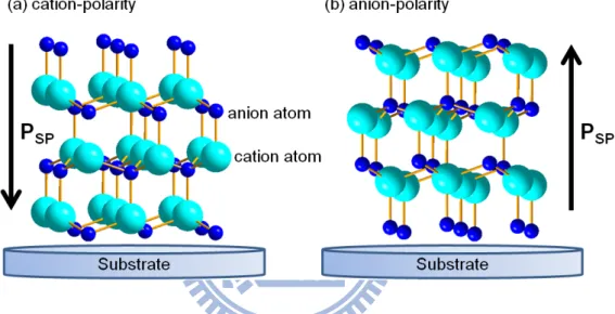
Si is a non-polar semiconductor. Whereas, III-nitrides wurtzite structures have two kinds of lattice polarities: cation (Al, Ga, In) polarity and anion (N) polarity. Because of large bond ionicity and crystalline asymmetry in c-axis. The direction of spontaneous polarization is from the cation atom to the nearest neighbor anion atom along the c axis, as shown in Fig. 1-1.
The main issue for polar III-nitrides grown on non-polar Si substrate is lattice polarity control. It was found that the surface morphology, chemical behavior, optical and electrical properties of III-nitrides are strongly dependent on the film polarity [4-7]. Several approaches, such as growth mode, substrate type, substrate nitridation, and variation of buffer layers, have been applied to control the polarity of III-nitrides film. In the case of GaN films, which were grown on sapphire by MBE technique using low-temperature-GaN, high-temperature-GaN, and low-temperature-AlN buffer layer, exhibit N-polarity. Ga-polarity was observed for films grown on high-temperature-AlN buffer layer. Compare to the studies of polarity control for III-nitrides grown on sapphire substrate, the study of polarity control for III-nitrides
grown on Si substrate is immature.
In addition to the polarity control, III-nitrides grown on Si substrate faces another important issue, large difference in the thermal expansion coefficients and lattice constant between Si and III-nitrides, which usually result in the residual strain and generation of misfit dislocations at the hetero-interfaces. This leads serious problems of wafer bending and crack formation, which will affect both the electrical and optical properties.
In order to solve part of these problems, growth on patterned Si substrates was proposed [8]. However, the time-consuming etching process to produce the patterned substrates and high-cost are the major drawbacks. To overcome these problems, K. Kusakabe et al. [9] have developed a novel and promising technique for the growth of GaN film on sapphire substrate by radio frequency plasma assisted MBE (RF-MBE). They have introduced a self-organized GaN nano-columns (NCs) structure as a buffer layer for subsequent GaN coalescence overgrowth. The cross-sectional SEM image of the overgrown GaN on NCs is shown in Fig. 1-2. The results of XRD and Raman scattering measurements suggest that GaN NCs effectively reduce the residual strain and reveal the free-standing properties of GaN films with 2.7 μm thickness. Recently, a numbers of groups have used this approach to improve the GaN films quality on
substrates thus far [16,17].
Recently, InN has successfully grown on Si substrates by using different growth technologies [18-27], e.g. insertion of different types of buffer layer between the Si substrate and InN epilayers. However, the quality of InN epilayers grown on Si substrates is still not good enough as compared with that grown on sapphire substrates by MBE [28]. Furthermore, the effect of polarity control on the crystal quality of InN film grown on Si(111) substrate by MBE is still not very clear. In this thesis, the coalescence overgrowth of GaN, InN nano-rods and the control the film polarity of InN on Si substrates are investigated.
This dissertation is divided into six chapters. Chapter 1 introduces the background and motivation of this study. Chapter 2 describes the experimental technique of MBE and the characterization methods. The epitaxial overgrowth of GaN nano-rods and InN nano-rods on Si(111) substrate are reported in Chapter 3 and Chapter 4, respectively. In Chapter 5, the effect of polarity control on the physical properties of InN thin films on Si(111) substrate is studied. Finally, Chapter 6 concludes this study.
Fig. 1-1 Atomic arrangement of two kinds of lattice polarities of III-nitrides: (a) cation ( Al, Ga, In )-polarity and (b) anion ( N )-polarity.
Chapter 2
Experimental details
In this chapter, we describe the plasma-assisted molecular beam epitaxy (PA-MBE) system used for growth of group-III nitride materials and various measurement techniques that were used to characterize the crystalline structure and optical properties. The measurements include x-ray diffraction, photoluminescence spectroscopy and micro-Raman spectroscopy.
2.1 Molecular Beam Epitaxy (MBE) system
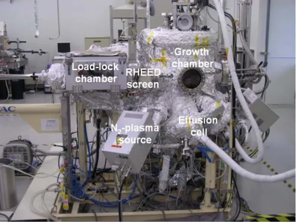
The MBE system is the ULVAC radio-frequency plasma-assisted MBE system with liquid nitrogen cryo-panels cooling, as shown in Fig. 2-1. The MBE system consists of a load-lock chamber and a growth chamber. The load-lock chamber was maintained at 1.5×10⁻⁸ torr by using a dry rotary pump and a turbo molecular pump.
The growth chamber was pumped down to a base pressure of 1.0×10⁻¹⁰ torr by a
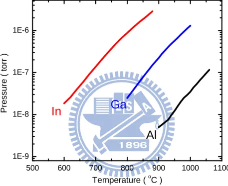
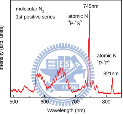
system was used to monitor the growth process. The filament current is set at 1.7A and the electron beam voltage is 20 kV. The group-III sources of aluminum (Al), gallium (Ga) and indium (In) were supplied by standard Knudsen effusion cells and the partial pressure of three different species is shown in Fig. 2-2. The group-V source of nitrogen radicals were generated in a ULVAC (RFS-1305A) radio frequency (RF) plasma source system with a frequency of 13.56 MHz and maximum of 500 W power. The optical emission spectrum of nitrogen plasma source is shown in Fig. 2-3. The emission lines at 745 and 821 nm are attributed to one of the 3s4P-3p4S0 and
3s4P-3p4P0 transitions of atomic nitrogen, respectively. The intensity of emission
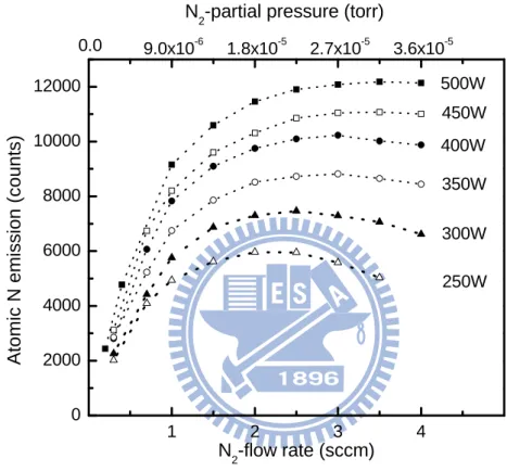
shows linear dependence on the RF-power (Fig. 2-4).
2.2 X-ray diffraction
Crystal with hexagonal structure can be described by in-plane lattice constant a and out of plane lattice constant c. The spacing d between the (h, k, l) planes can be written as: 2 2 2 2 2 2 3( ) 4 1 c l a k hk h d (1)
Where, h, k, l are the Miller indices. By using Bragg’s law; eq. (1) can be written as: 2 2 2 2 2 2 2 2
sin
4
)
(
3
4
1
c
l
a
k
hk
h
d
(2)Where, λ is wavelength of the x-ray. The lattice constants can be determined by XRD θ-2θ measurement. In this study, the Bede D1 HRXRD system equipped with a
X-ray source of Cu Kα1 line with the wavelength of 0.1540562 nm was used to
determine the crystal quality and lattice constants of group-III nitrides grown by MBE.
2.3 Photoluminescence
The 325 nm line (3.815 eV) of a He-Cd laser (Kimmon IK5552R-F) was used as the excitation light source for GaN (3.4 eV) PL measurement, and the emission from the GaN was analyzed by a SPEX 1403 double grating (1800 grooves/mm grating) spectrometer equipped with a thermal electric-cooled photomultiplier tube. An Ar+ laser operating at 488 nm (2.54 eV) was used as the excitation light source for InN (0.7 eV) photoluminescence measurement, The PL signal was analyzed by a SPEX-270M (600 grooves/mm grating) spectrometer detected using a liquid nitrogen cooled extended-InGaAs photodiodes detector equipped with lock-in amplification and a cutting wavelength at 2400 nm. The PL measurement system set-up is shown in Fig. 2-5 and Fig. 2-6. The schematic diagram of PL measurement systems includes the reflection mirrors, focusing lenses and sample cooling system. The samples were mounted on the copper holder and cooled in a closed-cycle refrigerator at a temperature near 10 K.
2.4 Micro-Raman scattering spectrometry
In this study, micro-Raman scattering was used to evaluate the residual strain of group-III nitrides. The micro-Raman scattering system set-up is shown in Fig. 2-7. The measurement at room temperature was carried out in backscattering geometry along the z direction (parallel to the c-axis of group-III nitrides). The 488 nm line of an Ar+-ion laser was used as the excitation source and focused through a microscope (Olympus BX41) objective into a spot of around 1 μm in diameter. The spectra were obtained using a Horiba Jobin-Yvon iHR550 (2400 grooves/mm grating) spectrometer equipped with a multichannel LN2-cooled charge-coupled device (CCD)
of 1024 × 256 pixels. The pixel size of 26 × 26 μm2 yields spectral resolution is 0.8
Fig. 2-1 The picture of major components of the ULVAC radio-frequency plasma-assisted molecular beam epitaxy system.
500 600 700 800 900 1000 1100 1E-9 1E-8 1E-7 1E-6
Al
Ga
Pressure ( tor r ) Temperature ( oC )In
Fig. 2-2 The partial pressure versus temperature of three different species (Al, Ga and In) effused by Knudsen-Cells.
500 600 700 800 atomic N 4 P-4S0 In tensi ty (a rb. units) Wavelength (nm) atomic N 4 P-4P0 821nm 745nm molecular N2 1st positive series
Fig. 2-3 Optical emission spectrum of N2 plasma with incident power 250W and
1 2 3 4 0 2000 4000 6000 8000 10000 12000 N
2-partial pressure (torr)
250W 300W 350W 400W 450W Atom ic N emission (co u n ts) N2-flow rate (sccm) 500W 0.0 9.0x10⁻⁶ 1.8x10⁻⁵ 2.7x10⁻⁵ 3.6x10⁻⁵
Fig. 2-4 Atomic nitrogen emission intensity at 745 nm as functions of the N2-flow
Chapter 3
Overgrowth of GaN thin film on GaN nano-rods
In this chapter, strain-free GaN thin film overgrowth on GaN nano-rods is realized by MBE on Si substrate. The strain-free condition was identified by the strong free A exciton (FXA) PL peak at 3.478 eV and the E2 high phonon Raman shift
of 567cm-1. The red-shift of PL peak energy and phonon Raman energy with
increasing the diameter of nano-rod result from the residual tensile stress in the overgrowth GaN layer. The residual tensile stress is generate from the nano-rods coalescence process. The density/diameter of GaN nano-rods increases/decreases with the growth temperature and the N/Ga ratio increase. It is clearly demonstrated that the critical diameter of GaN nano-rods is around 80nm for the overgrowth of strain-free GaN.
3.1 Growth of GaN nano-rods
3.1.1 Growth procedure of GaN nano-rods
Si(111) substrates by MBE system. Before growth, the Si(111) wafers were chemically cleaned by 10% HF to remove surface native oxides without rinsing in DI water to suppress oxide formation. After the chemical cleaning procedure, the Si substrate is mounted to substrate holder then loaded into the load-lock chamber. Prior to GaN nano-rods growth, the Si substrate was heated to 830oC to remove the residual
oxide in the substrate. In this case, a clear ( 7 × 7 ) surface reconstruction RHEED pattern was observed, as shown in Figs. 3-1 (a) and (b). After the thermal desorption, GaN nano-rods were then directly grown on Si (111) substrates under the nitrogen rich condition without any buffer layer. In order to investigate the effect of growth temperature and N/Ga ratio, one series of samples was designed and the detailed growth conditions are listed in Table 3-1. The variation of N/Ga flux ratio was adjusted by the beam equivalent pressure (BEP) of Ga. During the growth, the RF plasma power and nitrogen flow rate were kept constant at 500 W and 4.0 sccm, respectively.
3.1.2 Influence of growth parameters on GaN nano-rods
Fig. 3-1 (c) and (d) shows the surface reconstruction RHEED patterns of GaN nano-rods after the growth. The observation of in situ RHEED pattern shows that
Si(111) substrate plane. The three-dimensional growth morphology of GaN nano-rods can be identified by the spotty RHEED pattern. In contrast to GaN growth on sapphire, the observed RHEED patterns show that the GaN lattices do not rotate by 30° with respect to the Si surface. In other words, [11-20] direction of GaN is parallel to the [-110] direction of the Si (111) surface, and the [-1100] direction of GaN is parallel to the [11-2] direction of the Si (111) surface [8].
Fig. 3-2 (a) to (c) shows the plan and the tilted view SEM images of the GaN nano-rod with growth temperature from 800 oC to 860 oC. The morphology of the
GaN nano-rod grown on Si(111) depends strongly on the growth temperature. At the low growth-temperature (800 oC), the migration of Ga ad-atoms are substantially
suppressed. As a result, the initial nucleation seed density of nano-rods increases and the distance between the individual nano-rods decreases. Consequently, individual nano-rod coalesces into nano-rod bundles as shown in Fig. 3-2 (a). It is further confirmed by the spotty RHEED pattern as shown in Fig. 3-3 (a). In contrast, at high growth-temperature (830oC or 860oC), the migration of Ga ad-atoms is enhanced and
excess ad-atoms could be re-evaporated from Si(111) surface. Therefore, the coalescence phenomenon of individual nano-rod is absent and clear hexagonal surfaces are observed, as shown in Fig. 3-2 (b) and (c). Furthermore, at high growth-temperature, GaN nano-rods of twisted crystallographic alignment were
grown. As a result, the superposition of the elliptical RHEED patterns from incident electron beams of directions along the [-1100] and [11-20] azimuth of the hexagonal phase are observed [29], as shown in Fig. 3-3 (b) and (c).
The density/diameter of GaN nano-rods increases/decreases as growth temperature increases, as shown in Fig. 3-2 (a) to (c). The high growth-temperature increases the surface mobility of ad-atoms, which leads to easier formation of small nucleation seeds. On the other hand, the height of GaN nano-rods increases with the growth-temperature because the size of nucleation seed is smaller and the migration length of surface ad-atoms is enhanced at high temperature. When equally providing the Ga and N atoms, the height of GaN nano-rod with smaller nucleation seed is higher than the height of GaN nano-rod with larger nucleation seed.
Fig. 3-4 (a) to (c) shows tilted and plan view SEM images of the self-assembled GaN nano-rod grown on Si(111) with different Ga BEP from 2.8×10⁻⁸ to 2.0×10⁻⁷ torr
at growth-temperature of 830 oC. By decreasing the Ga BEP from 2.0×10⁻⁷ to 2.8×10⁻⁸
torr, the density/diameter of GaN nano-rod increases/decreases. In addition, the height decreases as the Ga BEP of GaN nano-rod decreases. This phenomenon is due to the sufficient surface energy of surface ad-atom to incorporate and re-evaporate at high growth-temperature. However, decreasing the Ga atom reduces the probability of
the other hand, the height of GaN nano-rods decreases as the Ga BEP decreases. This is because the GaN nano-rod increases but without enough Ga atom, the height of GaN nano-rod would be decreased.
3.1.3 X-ray analysis
Fig. 3-5 show XRD patterns of the vertically aligned GaN nano-rods grown under the different growth conditions. The diffraction peak at 34.56 degree is indexed as (0002) of the wurtzite GaN structure, indicating that the single crystal GaN nano-rods are preferentially oriented in the c-axis direction. From the diffraction peak position of GaN (0002), the c-axis lattice constant of GaN nano-rods is estimated to be 5.185±0.001 angstrom. This value of c-axis lattice constant is identical to that of free-standing GaN layer, indicating that GaN nano-rods exhibit the free standing properties.
3.1.4 Raman measurement
Fig. 3-6 show the room-temperature Raman spectrum of the vertically aligned GaN nano-rods grown under the different growth conditions. The Raman peak position of E2 mode is known to be sensitive to the residue stress in the GaN film [30]. According to the previous report [31], the E2 mode of free-standing and
homo-epitaxially grown GaN appears at 567.0±0.1 cm-1. If this value is a reference
for an strain-free GaN, we can conclude that the all of GaN nano-rods are strain-free and in agreement with our XRD measurement. The measured wurtzite GaN E2 high mode at 567 cm-1 also support that GaN nano-rods are strain-free.
3.1.5 Conclusions of GaN nano-rods
The morphology of GaN nano-rods strongly depends on growth condition, i.e. growth temperature and N/Ga ratio. As the growth-temperature increases, the density of GaN nano-rods increases, the diameter of GaN nano-rods decreases and the height of GaN nano-rods increase. As the BEP of the Ga increases from 2.8x10⁻⁸ to 2.0x10⁻⁷
torr, the density of GaN nano-rods reduces whereas the diameter of GaN nano-rods increases. As a consequence, we can control the density and diameter of GaN nano-rods by growth-temperature and N/Ga ratio. From the results of XRD and Raman measurements, one can conclude that all GaN nano-rods are strain-free.
3.2 GaN thin film overgrowth on GaN nano-rods
3.2.1 Growth procedure of GaN thin film
nitrogen cryo-panel cooling. The 2-inch Si (111) wafers (p-type doping) were chemically cleaned by 10% HF without rinsing in DI water to suppress oxide formation. A clear Si (7×7) surface reconstruction was observed by the reflection high-energy electron diffraction (RHEED) at a substrate temperature of 830oC. The
GaN nano-rods were then directly grown on Si (111) substrates at 850oC without any
buffer layer under different III/V ratios to control the diameters of GaN nano-rods. During the growth, the RF-plasma power and nitrogen flow rate were kept constant at 500 W and 4.0 sccm, respectively. The variation of III/V flux ratio was adjusted by the gallium flux. The gallium flux was varied from 9.0×10⁻⁸, 2.0×10⁻⁷ to 3.7×10⁻⁷ torr
for samples F, G, and H, respectively. The respective rod diameters of 60, 80, and 90 nm were investigated by JEOL JSM-7001F scanning electron microscopy (SEM). After the growth of GaN nano-rods, the gallium flux was increased to 9.7×10⁻⁷ torr to
enhance the lateral growth rate for the growth of the overgrowth GaN layers. The surface morphologies and crystalline quality of GaN nano-rods are studied by SEM and X-ray diffraction spectrum analysis, respectively. Photoluminescence and micro-Raman scattering are used to characterize the optical properties.
3.2.2 Structural properties
GaN with different rod diameters. The diameters are (a) 60nm, (b) 80 nm and (c) 90 nm, respectively. The N-rich nano-rod layers and the Ga-rich overgrowth layers can be clearly identified from the cross-section SEM images of Fig. 3-7. As the Ga flux was increased, the lateral overgrowth was enhanced. For sample F, the overgrowth GaN forms irregular terraces and without fully coalescence as shown in Fig. 3-7 (a). By increasing the diameters of nano-rods, the gaps between the nano-rods decrease. The GaN terraces merge together to show better surface morphology in Fig. 3-7 (b) and (c). The cross-sectional SEM image of sample G shows that the film is not continuous in lateral direction, and from boundaries gaps. From the top-view SEM image, one can see the spacing gradually shrunk as the diameter of nano-rods was increased and the area of the terrace was also increased, as show in Fig. 3-7 (b). The further increasing diameter of nano-rods results in continuous morphology in cross-section of sample H as shown in Fig. 3-7 (c). In Fig. 3-7 (c), the top-view SEM image shows that the overgrowth layer in sample H is not completely continuous, with pronounced trenches and some pits.
3.2.3 Optical properties
is primarily from the overgrowth layer. All three spectra are dominated by the strong narrow near-band-edge (NBE) excitonic emission near 3.47 eV and a weak broad emission from 3.32 eV to 3.42 eV. No deep-level emission or yellow-band transition at 2.3 eV was detected. The two main peaks of the weak emission band are assigned to the excitons bound to surface defect (Y2 ) and the shallow donor-acceptor pair
( DAP ) located on surface (Y6) [34]. The broad emission is relatively weak in sample
H, which has smooth surface morphology. It implies that the density of surface defects is small for the smooth surface.
In order to further identify the emission mechanism, the temperature-dependent PL experiments at temperature range from 10 to 120 K are presented in Fig. 3-9. In Fig. 3-9, the weak shoulder at 3.485 eV is attributed to the free B exciton transition (FXB). The strongest peak at 3.478 eV is identified as the free A exciton transition
(FXA). The peak at 3.472 eV results from the recombination of exciton bound to
neutral donor (D0X). The energy red-shift with temperature of FX
A follows the
Vashini’s equation. For D0X peak, the intensity decrease abruptly due to the thermal
excitation to higher energy FXA state. The thermal quenching of the donor-bound
exciton (D0X) peak occurs at 80–100 K [35]. For sample F and G, the energy position
of FXA at 3.478 eV implies that the overgrowth GaN is strain-free [36]. The FXA
of defects, which was only observed in high-quality single-crystal nano-rod [37]. On the other hand, the PL spectrum of sample H was dominated by the D0X transition at
3.466 eV, shown in Fig. 3-9 (c). Compare with the energy position of D0X of sample
F and G, the energy of D0X for sample H red-shifts 6 meV. This indicates that the
overgrowth GaN of sample H has tensile strain. By using the value of the proportionality factor K= 21.2 meV/GPa [38] for the strain-induced PL peak shift, a residual stress of 0.28 GPa built in the overgrowth layer can be estimated.
The tensile strain in these specimens was also investigated by the micro-Raman spectroscopy by measuring the frequency position of the E2-high phonon mode. The
normalized E2-high mode of these specimens measured at room temperature is shown
in Fig. 3-10. The peak of Raman shift in sample F, G and H are 567.0 cm-1, 567.0 cm-1
and 565.7 cm-1, respectively. The energy positions of E
2-high peak for sample F and
sample G are at 567.0 ± 0.1 cm-1, which is believed to be the E
2-phonon from
strain-free GaN [39].The energy difference in the Raman shift between sample H and sample F (and sample G) is 1.3 cm-1. The residual stress could be calculated based on
the stress coefficient of 4.24 cm-1GPa-1 [39]. The estimated residual stress in the
overgrowth GaN layer of sample H is 0.30 GPa, which is quite consistent with the result of PL spectral shift. The red-shift of PL peak energy and Raman shift value in
3.2.4 X-ray analysis
This residual stress can be further checked by measuring the X-ray 2θ-scan of (0002) diffraction. The respective peak positions of XRD for samples F, G, and H are at 34.560 o, 34.560 o, and 34.574 o, as shown in Fig. 3-11. The calculated c-axis lattice
constant of sample F, G and H which are 5.1844 Ǻ, 5.1844 Ǻ and 5.1824 Ǻ, respectively. The c-axis lattice constant of sample F and sample G are 5.1844 Ǻ are very close to the strain-free value of c0 = 5.185 Ǻ. The smaller c-axis lattice constant
of sample H indicates the existence tensile strain in the c-plane of GaN. The in-plane stress (σ) of GaN grown on Si can be described by the lattice strain (ε) from the relationship σ=Mε, where M is the biaxial elastic modulus of GaN. When the hexagonal GaN is bi-axally stressed on Si, its in-plane lattice deformation (εa) is
associated with out-of-plane lattice (εc) change as described by the relationship εc= -
2(C13/C33)εa, where εc = ( c - c0 ) / c0 and C13, C33 are elastic constants of GaN [41].
The in-plane biaxial stress in sample H can be calculated by using M = 449 GPa, C13
= 103 GPa, and C33 = 405 GPa [42], respectively. The estimated biaxial tensile stress
in the c-plane of sample H is 0.24 GPa, which is quite consistent with the results of PL and Raman measurements. Therefore, we consider that the tensile stress is generate from the coalescence process [43]. From the results of PL, Raman and XRD measurement, one can conclude that residual strain will exist in the GaN overgrowth
on GaN nano-rods of diameter larger than 90 nm. This indicates that only suitable diameter of GaN nano-rod can use as a buffer layer for overgrowth strain-free GaN layer.
3.3 Conclusions
In summary, we have demonstrated the growth of high quality coalescence overgrowth GaN nano-rods on Si (111) substrate with RF-MBE. By using the temperature-dependent PL experiments and micro-Raman spectroscopy, the critical diameter of GaN nano-rods for strain-free GaN overgrowth is around 80-90 nm. The residual stress which exists in GaN overgrown on GaN nano-rods with 90 nm of diameter is about 0.3 GPa.
Table 3-1 The growth conditions of GaN nano-rods
Growth Temp. (oC) BEP Ga (Torr) N2 plasma (W/sccm) Growth time (min) Sample A 800 2.0x10⁻⁷ 500/4.0 120 Sample B 830 2.0x10⁻⁷ 500/4.0 120 Sample C 860 2.0x10⁻⁷ 500/4.0 120 Sample D 830 7.1x10⁻⁸ 500/4.0 120 Sample E 830 2.8x10⁻⁸ 500/4.0 120 Sample F 850 9.0x10⁻⁸ 500/4.0 120 Sample G 850 2.0x10⁻⁷ 500/4.0 120 Sample H 850 3.7x10⁻⁷ 500/4.0 120Fig. 3-1 Evolution of RHEED patterns for the growth process of vertically aligned GaN nano-rods grown on Si(111) substrate. (a) and (b) are clean Si(111) - ( 7 × 7 ) reconstruction surface after thermal desorption. (c) and (d) are RHEED patterns of GaN nano-rods after the growth. The incident electron beam directions are along Si[11-2] (∥GaN [-1100]) and Si[-110] (∥GaN [11-20]) directions, respectively. (e)
Fig. 3-2 SEM images in the tilted (left) and plan (right) views of the vertically aligned GaN nano-rods grown on Si(111) at the same V/III ratio with growth temperature at (a) 800oC, (b) 830oC, and (c) 860oC, respectively. The scale bar
Fig. 3-3 RHEED patterns of GaN nano-rods with growth temperature at (a) 800oC, (b)
830oC, and (c) 860oC, respectively. The incident electron beam directions are along
Fig. 3-4 SEM images in the tilted (left) and plan (right) views of the vertically aligned GaN nano-rods grown on Si(111) at growth temperature 830oC with BEP of
(a) Ga= 2.0×10⁻⁷ torr, (b) Ga= 7.1×10⁻⁸ torr and (c) Ga = 2.8×10⁻⁸ torr, respectively.
33.0 33.5 34.0 34.5 35.0 35.5 36.0 33.0 33.5 34.0 34.5 35.0 35.5 36.0 BEPGa=2.0x10⁻⁷torr 34.56 GaN (0002) TG=800oC T G=830 o C TG=860oC
XRD Intensity (arb. units)
2 (degree) 33.0 33.5 34.0 34.5 35.0 35.5 36.0 33.0 33.5 34.0 34.5 35.0 35.5 36.0 TG=830oC BEPGa=2.8x10⁻⁸torr BEP Ga=7.1x10 -8 torr BEP Ga=2.0x10 -7 torr GaN (0002) 34.56 XR D Intensi ty (arb. units ) 2 (degree)
532 539 546 553 560 567 574 581 588 532 539 546 553 560 567 574 581 588 BEP Ga=2.0x10 -7 torr T G=800 o C T G=830 o C GaN E2(high) 567 cm-1
Raman Intensity (arb. units)
Raman shift (cm-1) T G=860 o C 532 539 546 553 560 567 574 581 588 532 539 546 553 560 567 574 581 588 TG=830oC BEPGa=2.8x10⁻⁸torr BEPGa=7.1x10⁻⁸torr GaN E2(high) 567 cm-1
Raman Intensity (arb. units)
Raman shift (cm-1) BEPGa=2.0x10⁻⁷torr
Fig. 3-7 SEM images in the cross-sectional ( left ) and top ( right ) view of the overgrowth sample. The diameters of samples are (a) 60nm, (b) 80 nm and (c) 90 nm, respectively. The scale bars are 1 μm.
2.0
2.5
3.0
3.5
2.0
2.5
3.0
3.5
Y2 Y6 Y 6 (c) sample H (b) sample GPL intensity (arb. units)
Photon energy (eV)
(a) sample F
Y
2
3.44
3.46
3.48
3.50
3.44
3.46
3.48
3.50
D0X
Photon energy (eV)
(c) sample H D0X
PL intensity
(arb. units
)
(b) sample G FXB FXA FXB FXA (a) sample F D0XFig. 3-9 Temperature-dependent PL spectra of three samples at temperature range from 10 to 120 K.
546 553 560 567 574 581 588 546 553 560 567 574 581 588 Raman intensity(arb.units) Raman shift (cm-1) sample F sample G sample H E2(high)
34.4 34.5 34.6 34.7 101 102 103 104 34.4 34.5 34.6 34.7 (H) (G)
XRD Intensity (arb. units)
2 (degree)
(F)
Chapter 4
Overgrowth of InN thin film on InN nano-rods
In this chapter, we studied the spontaneous growth of InN nano-rods on Si(111) substrate by MBE. The morphology of InN nano-rods mainly affected by the N/In ratio and the growth temperature. The coalescence-overgrowth of high quality InN film on InN nano-rods, which were grown on Si(111) substrate, is demonstrated. However, due to the poor adhesion between the nano-rods and the Si substrate, film delimitation and cracking occurs during growth. From the result of PL measurement, we found that the InN film quality has been improved comparing to the InN films grown on AlN buffer and Si(111) substrate.
4.1 Growth of InN nano-rods
4.1.1 Growth procedure of InN nano-rods
The InN nano-rods and the overgrowth InN layers were grown sequentially on Si(111) substrates by MBE system. The 2-inch Si(111) wafers (p-type doping) were chemically cleaned by 10% HF before loading into the MBE chamber. Surface oxides
were subsequently removed in situ by heating the substrate to 830 °C. The substrate temperature was lowered to 480–510 °C for the growth of InN nano-rods. The InN nano-rods were directly grown on Si(111) without any buffer layer under different III/V ratio and substrate temperature. After the growth of InN nano-rods, the indium flux was increased to 4.61×10⁻⁷ torr to enhance the lateral growth rate. The substrate
temperature was then increased to 560oC to improve the surface migration ability of
indium ad-atom for the overgrowth InN thin film. During the growth, the RF-plasma power and nitrogen flow rate were kept constant at 500 W and 4.0 sccm, respectively. The variation of III/V flux ratio was adjusted by the indium flux. In this study, the indium flux was varied from 4.40×10⁻⁹ to 6.77×10⁻⁷ torr The growth parameters for
the investigated samples are given in Table 4-1. The surface morphologies and crystalline quality of GaN nano-rods are studied by SEM and X-ray diffraction spectrum analysis, respectively. The optical properties are characterized by the photoluminescence measurement.
4.1.2 Influence of growth parameters on InN nano-rods
Fig. 4-1 shows the RHEED patterns of the growth process of the InN nano-rods grown on Si(111) substrate. The clear 7×7 RHEED pattern [Fig. 4-1(a)] indicate a
4-1(d) shows the RHEED patterns of InN nano-rods after growth. The result indicates that the crystal lattice of InN nano-rod corresponds to the wurtzite-type single crystal. In addition, the nano-rod growth direction (rod axis) is along the wurtzite c-axis and well aligned vertically. The spotty ring-like RHEED feature is a consequence of three-dimensional growth morphology and twisted crystallographic alignment between individual nano-rods in the growth plane.
In order to obtain the optimum growth-condition, the growth of InN nano-rods was controlled by the growth temperature and the In-flux. The dependence of the InN nano-rods morphology on In flux is shown in Fig. 4-2 and Fig. 4-3. These samples have been deposited at 480 oC for 120 min. At low growth-temperature and lower
In-flux (BEPIn=4.40×10⁻⁹ torr), the nano-rods grow with a lower aspect ratio, i.e. like
nano-disk. This phenomenon is due to the migration ability of In atom at low-temperature was suppressed. As the In-BEP increases to 1.45×10⁻⁸ torr the
density and aspect ratio of InN nano-rods is increasing and but the height of nano-rods is still short [Fig. 4-2 (a) and (b)]. Further increase of the In-flux to 4.85×10⁻⁸ torr
results in a high density of short columns [Fig. 4-2 (c)]. When the In-flux increases to 1.31×10⁻⁷ torr, high density of longer nano-rods were produced, as shown in Fig.
4-3(a). However, due to the lower growth-temperature, the InN nano-rods are not separate obviously. As the In-flux increases further, the InN nano-rods were merged
and result in rough surface as shown in Fig. 4-3 (b). The morphologies of InN grown at low-temperature and higher In flux, closely compact InN island structures were formed as shown in Fig. 4-3 (c).
Fig. 4-4 show the well-separated InN nanorods grown at high growth-temperatures (510 °C), with appropriate In-flux. The individual InN nano-rod shows a distinct hexagonal rod shape. This phenomenon is caused by the sufficient surface energy of surface ad-atom to incorporation and re-evaporation at high growth-temperature.
4.1.3 X-ray analysis
Fig. 4-5 shows the XRD pattern of the InN nano-rods grown at 510oC with
BEPIn=1.31×10⁻⁷ torr. We observed two diffraction peaks indexed as Si(111) substrate
and wurtzite InN(0002), indicating that InN nano-rods are single crystal and preferentially oriented in the c-axis direction. From the diffraction peak position of InN(0002), we can estimate the c-axis lattice constant of InN nano-rods is 5.700 Å. This value of c-axis lattice constant is close to the free-standing InN layer [44], indicating that InN nano-rods exhibit nearly free-standing property. Due to the high aspect ratio of the nano-rod structure, the residual strains are likely to be localized at
are strain-free.
4.2 InN thin film overgrowth on InN nano-rods
4.2.1 Growth procedure of InN thin film
The successful experience of strain free and high quality GaN-layer overgrowth on GaN nano-rods encourages us to try this approach to growth high quality InN layer on Si substrate. However, InN-layer overgrowth on InN nano-rods results in significant film delimitation and cracking, as shown in Fig. 4-6. It is due to the poor adhesion between the rod and the Si substrate [as shown in Fig.4-4(a)]. When the layer is almost fully coalesced, tensile stress of approximately 0.2 GPa [45] has been observed by Abhishek Jain et al.. The tensile stress results in crack propagation along the interface between substrate and rods.
4.2.2 Optical properties
Fig. 4-7 shows the PL spectrum of InN layer overgrown on InN nano-rods. With comparison to the InN layer grown on the AlN/Si(111) substrate at the same growth-condition. It was found that the emission peak energy of InN red shifts from 0.83 eV to 0.75 eV, and the FWHM reduces from 150 meV to 110 meV. It implies that the film quality of InN-overgrown on InN nano-rods is effectively improved.
4.3 Conclusions
In summary, we have demonstrated the growth of coalescence overgrowth InN nano-rods on Si(111) substrate with RF-MBE. Due to the poor adhesion between the rod and the Si substrate, film delimitation and cracking occurs during growth was observed. However, the result of PL measurement indicates the InN film quality has been improved comparing to that of InN film grown on AlN/Si(111) substrate.
Table 4-1 The growth conditions of InN nano-rods
Growth Temp. (oC) BEP In (Torr) N2 plasma (W/sccm) Growth time (min) Sample A 480 4.4x10⁻⁹ 500/4.0 120 Sample B 480 1.4x10⁻⁸ 500/4.0 120 Sample C 480 4.8x10⁻⁸ 500/4.0 120 Sample D 480 1.3x10⁻⁷ 500/4.0 120 Sample E 480 3.0x10⁻⁷ 500/4.0 120 Sample F 480 6.7x10⁻⁷ 500/4.0 120 Sample G 510 4.8x10⁻⁸ 500/4.0 120 Sample H 510 1.3x10⁻⁷ 500/4.0 120Fig. 4-1 RHEED patterns for the growth process of InN nano-rods on Si(111): (a) Si(111)−(7×7) reconstruction surface; (b) After 30 sec InN nano-rods growth reconstruction surface; (c) After 30 min InN nano-rods growth; (d) The ending of InN nano-rods growth.
Fig. 4-2 SEM images in the top ( left ) and cross-sectional ( right ) view of the InN nano-rods grown on Si(111) at growth temperature 480oC with BEP of (a) In =
4.40×10⁻⁹ torr, (b) In = 1.45×10⁻⁸ torr and (c) In = 4.85×10⁻⁸ torr. The scale bar
Fig. 4-3 SEM images in the top ( left ) and cross-sectional ( right ) view of the InN nano-rods grown on Si(111) at growth temperature 480oC with BEP of (a) In =
1.31×10⁻⁷ torr, (b) In = 3.06×10⁻⁷ torr, and (c) In= 6.77×10⁻⁷ torr. The scale bar
Fig. 4-4 SEM images in the top ( left ) and cross-sectional ( right ) view of the vertically aligned InN nano-rods grown on Si(111) at growth temperature 510oC with
BEP of (a) In= 4.85×10⁻⁸ torr and (b) In= 1.31×10⁻⁷ torr. The scale bar represents 500
28 29 30 31 32 33 34 103 104 105 106 28 29 30 31 32 33 34 InN (0002) 31.36 Si(111) 28.44 XRD intensity(arb. units) 2 (degree)
Fig. 4-5 X-ray diffraction pattern of InN nano-rods of sample H, indicating that the nano-rods are single crystal wurzite structure.
Fig. 4-6 SEM images of the cracking InN layer after overgrowth on InN nano-rods: (a)top view and (b) cross-sectional view of the InN cracking layer. The scale bar represents 1μm.
0.6 0.7 0.8 0.9 1.0 1.1 0.6 0.7 0.8 0.9 1.0 1.1 InN/InN rod/Si InN/AlN/Si PL In te nsiny (arb . units)
Photon energy (eV)
10 K
Fig. 4-7 Normalized PL spectrum of InN layer overgrowth on InN nano-rods and InN layer growth on AlN/Si(111) substrate at the same growth conditions.
Chapter 5
Polarity control of InN thin film on Si(111) substrate
In this chapter, polarity control of In- and N-polar InN layers grown on Si(111) substrate by MBE were studied. We found that the lattice polarity of InN can be controlled by the thickness of initial Al-layer that were deposited prior to AlN buffer layer. A change from N-polar to In-polar was observed when Al-layer exceeded one monolayer (ML). In this study, the lattice polarity of InN was determined by wet chemical etching. In the case of N-polar InN, the sample’s surface became rough and pyramids appeared after etching. On the other hand, the surface of In-polar InN remained smooth and pits appeared after etching.
5.1 Growth procedure
All specimens studied in this chapter were grown on Si(111) substrates by MBE and the growth process was monitored by RHEED. The 2-inch Si(111) wafers (p-type doping) were chemically cleaned by 10% HF to remove surface native oxides. After the chemical cleaning procedure, the Si substrates were mounted to substrate holder
then loaded into the load-lock chamber. Before growth, the Si substrates were thermally desorbed at 830oC until a clear 7 × 7 surface reconstruction RHEED pattern
was observed, as shows in Fig. 5-1 (a). It indicates that the native oxides have been completely dissolved from the Si(111) substrate surface. The Al pre-seeding layer was then deposited on Si surface with various deposition time and temperature prior to AlN buffer layer growth. After AlN buffer layer grown at 850oC, the substrate
temperature was lowered to 440–580 °C for the growth of InN layers. The BEP of Al flux is 3.49×10⁻⁸ torr was obtained by heating Al cell at 1000oC. The BEP of In flux is
4.61×10⁻⁷ torr by heating In cell at 800oC. The Nitrogen flow rate/plasma power for
growing AlN buffer layer and InN epilayer on Si were 0.7sccm/250W and 1.5sccm/500W, respectively. In order to study the influence of the initial thickness of Al-layer on the lattice polarity, two samples were designed. The thickness of Al-layer of Sample A and B were 0.6ML and 1.0 ML, respectively. The polarity of InN films were determined by chemical wet etching, 90 min at room temperature using 10 mol/l KOH solution [46].
5.2 Results and Discussion
discussed. Recently, X. Y. Liu et al. [47] investigated the polarity of GaN layer grown on Si(111). It was found that the polarity depends on the thickness of initially deposited Al-layers before the growth of AlN buffer layer. Above 1.3 ML of Al-layer, the Ga-polar film is obtained. Otherwise, the film is N-polar.
According the previous study of polarity control of GaN [47], the InN polarity was also controlled by adjusting the thickness of Al initial deposition layer. Fig. 5-1 shows the real time RHEED patterns of Sample A surface under the Al beam exposure of 0, 10 and 20 sec at 850°C. Fig. 5-1 (a) is the clean Si (111) 7×7 pattern at the substrate temperature of 850°C. After Al exposure of 10 sec with the BEP of 3.49×10⁻⁸ torr, √3×√3 pattern appeared, as shown in Fig. 5-1 (b). In previous report, √3×√3 phase of Al on Si (111) was observed with the Al coverage of 1/3 ML and each Al atom terminates three Si dangling bonds [48]. After Al exposure of 20 sec, sharp streaks accompanying sub-streaks were observed. The pattern remains the same after long exposure to Al beam [Fig. 5-1 (c)]. The pattern was attributed to the so-called Al/Si (111) γ-phase, which indicates the saturated phase with the coverage of 0.6 ML Al-layer [49]. Fig. 5-1 (d) shows the streaky RHEED pattern of AlN buffer layer grown on Si(111) at 850oC. The streaky RHEED pattern suggests a
two-dimensional growth mode and a smooth surface. Subsequently, the substrate temperature was decreased to 560oC for the growth of InN film. Fig. 5-1 (e) shows the
streaky RHEED pattern of InN film.
According to the phase formation diagram of Al on Si (111), only 1 ML of Al-layer can be deposited on Si(111) surface for the temperature above 600oC [50]. In
order to deposit more than 1 ML on Si (111), low-temperature-growth below 600 °C is required. Fig. 5-2 (a) and (b) show RHEED patterns of Sample B surface under the Al beam exposure of 0 and 60 sec at 600 °C, respectively. Compared to the clean surface of Fig. 5-2 (a), the 7×7 fractional diffraction streaks disappeared completely in Fig.5-2(b). It implies the formation of Al islands when the Al beam exposure exceeding 60 sec, thickness of Al-layer is more than 1 ML. After the growth of 60 sec Al-layer, the growth of AlN was started. RHEED pattern obtained after 200 sec of AlN deposition at 600 °C was shown in Fig. 5-2 (c). It is more diffusive as compared to the sharp streak patterns observed on the AlN buffer. After 200 sec of low temperature AlN deposition, 60 min of AlN buffer growth was started by increasing the temperature up to 850oC. Fig. 5-2 (d) shows the spotty RHEED pattern of AlN
buffer layer grown at 850oC, which indicates the three-dimensional growth mode and
rough surface. Subsequently, the growth temperature was decreased to 460C for the growth of InN layer. Fig. 5-2 (e) shows the RHEED pattern after the growth of InN layer at 460oC.
for 90 min at room temperature. After etching, polygonal structures were observed in sample A, as shown in Fig. 5-3(b). However, for sample B, the sample surface was more smooth after etching, as shown in Fig. 5-4(b). The appearance of polygonal structures was attributed to the N-polarity. On the other hand, smooth surface is the character of In-polarity InN. Therefore, we concluded that the polarity of InN layers can be changed from N-polarity to In-polarity by increasing the thickness of Al initial deposition layer prior to the growth of the AlN buffer layer.
In order to understand the change of lattice polarity on the initially deposited Al-layer, the following growth mechanism is proposed. The selection of AlN polarity is schematically shown in Fig. 5-5. The polarity of AlN grown on the Al covered surface depends on bonding configuration among N atoms and Al atoms. If the N atom takes position A, Al polarity occurs; if the N atoms take position B, N polarity occurs. When a N atom enters position B, it needs to cooperate three Al atoms. Therefore, the formation of the N-polarity bonding configuration seems kinetically unfavorable process on the Al covered surface [51].
5.3 Conclusions
In summary by controlling the thickness of initially deposited Al-layer prior to AlN buffer layer, we demonstrated that the polarity of InN thin films on Si(111)
substrate by PA-MBE. The InN thin film changed from N-polar to In-polar when Al layer exceeding one ML. The lattice polarities of InN layers were determined by chemical wet etching. N-polar InN surface is rough and pyramid structure exist after etching. However, the surface of In-polar InN is smooth.
Fig. 5-1 RHEED patterns of Si (111) at 850 °C exposed to Al beam for (a) 0 sec, (b) 10 sec, (c) 20 sec, (d) after 60 min AlN growth and (e) after 2hr InN deposition at 560oC. The incident electron beam directions are along Si[11-2] (∥AlN [-1100]) and
Fig. 5-2 RHEED patterns of Si (111) at 600 °C, exposed to Al beam for (a) 0 sec, (b) 60 sec, (c) after 200 sec AlN deposited, (d) after 60 min AlN growth and (e) after 2hr InN deposition at 460oC. The incident electron beam directions are along Si[11-2]
Fig. 5-3 The SEM images of sample A before and after etching in a 10 mol/l KOH solution at room temperature.
Fig. 5-4. The SEM images of sample B before and after etching in a 10 mol/l KOH solution at room temperature.
\
Chapter 6
Conclusion
In this dissertation, the spontaneous growth of GaN and InN nano-rods on Si(111) substrate by PA-MBE were studied. In the case of GaN nano-rods, the morphology of nano-rods strongly affected by the N/Ga ratio and the growth temperature. The density/diameter of GaN nano-rods increases/decreases with the growth temperature and the N/Ga ratio increase. From the results of XRD and Raman measurements, one can conclude that nano-rods are strain-free single crystals.
For the case of InN nano-rods, we demonstrate that vertically aligned InN nano-rods can be grown on Si(111) by PA-MBE. From the results of XRD one can conclude that nano-rods are strain-free single crystals.
In addition, strain-free GaN overgrown on GaN nano-rods on Si substrate is realized. The strain-free condition was identified by the strong free A exciton (FXA)
photoluminescence (PL) peak at 3.478 eV and the E2 high phonon Raman shift of 567cm-1. It is clearly demonstrated that the critical diameter of GaN nano-rods is
and phonon Raman energy with decreasing the diameter of nano-rod result from the strain relaxation of overgrowth GaN.
On other hand, InN overgrowth on InN nano-rods on Si (111) substrate, exhibit film delimitation and cracking occurs during growth. Due to the poor adhesion between the rod and the Si substrate, However, from the result of PL measurement, we found that the InN film quality has been enhanced compare to the growth on AlN/Si(111) substrate.
Furthermore, In- and N-polar InN layers grown on Si(111) substrate by MBE were investigated. We found that the lattice polarity of InN can be controlled by the thickness of initial Al-layer that were deposited prior to AlN buffer layer. A change from N-polar to In-polar was observed when Al-layer exceeded one monolayer (ML). In this study, the lattice polarity of InN was determined by chemical wet etching method. In the case of N-polar InN, the sample’s surface became rough and pyramids appeared after etching. On the other hand, In-polar InN remained smooth surface.
Reference:
[1] K. Xu and A. Yoshikawa: Appl. Phys. Lett. 83, 251 (2003).
[2] J. Wu and W. Walukiewicz: Superlattices Microstructures, 34, 63 (2003).
[3] J. Wu, W. Walukiewicz, K.M. Yu, J.W. Arger III, E.E. Haller, H. Lu, W.J. Schaff, Y. Saito and Y. Nanishi: Appl. Phys. Lett. 80, 3967 (2002).
[4] A. R. Smith, R. M. Feenstra, D. W. Greve, M.-S. Shin, M. Skowronski, J. N eugebauer and J. E. Northrup: Appl. Phys. Lett. 72, 2114 (1998).
[5] G. Tamulaitis, I. Yilmaz, M. S. Shur, R. Gaska, C. Chen, J. Yang, E. Kuokstis, A. Khan, S. B. Schujman and L. J. Schowalter: Appl. Phys. Lett. 83, 3507 (2003). [6] Hajime Okumura, Mitsuaki Shimizu, Xu Qiang Shen and Toshihide Ide: Current
Applied Physics 2, 305 (2002).
[7] O. Ambacher, J. Smart, J.R. Shealy, N.G. Weimann, K. Chu, M. Murphy, W.J. Schaff, L.F. Easterman, R. Dimitrov, L. Wittmer, M. Stutzmann, W. Rieger and J. Hilsenbeck: J. Appl Phys. 85, 3222 (1999).
[8] A. Krost and A. Dadgar: Mater. Sci. Eng. B 93, 77 (2002).
[9] K. Kusakabe, A. Kikuchi and K. Kishino: Jpn. J. Appl. Phys. 40, L192 (2001). [10] L. Meshi, D. Cherns, I. Griffiths, S. Khongphetsak, A. Gott, C. Liu, S.
Denchitcharoen, P. Shields, W. Wang, R. Campion, S. Novikov and T. Foxon: Phys. Status Solidi C 5, 1645 (2008).
[11] D. Cherns, L. Meshi, I. Griffiths, S. Khongphetsak, S.V. Novikov, N. Farley, R.P. Campion and C.T. Foxon: Appl. Phys. Lett. 92, 121902 (2008).
[12] C.L. Chao, C.H. Chiu, Y.J. Lee, H.C. Kuo, P.-C. Liu, J.D. Tsay and S.J. Cheng: Appl. Phys. Lett. 95, 051905 (2009).
[13] Q. Li, Y. Lin, J.R. Creighton, J.J. Figiel and G.T. Wang: Adv. Mater. 21, 2416 (2009).
[14] T.-Y. Tang, W.-Y. Shiao, C.-H. Lin, K.-C. Shen, J.-J. Huang, S.-Y. Ting, T.-C. Liu, C.C. Yang, C.-L. Yao, J.-H. Yeh, T.-C. Hsu, W.-C. Chen, H.-C. Hsu and L.-C. Chen: J. Appl. Phys. 105, 023501 (2009).
[15] Y.-S. Chen, W.-Y. Shiao, T.-Y. Tang, W.-M. Chang, C.-H. Liao, C.-H. Lin, K.-C. Shen, C.C. Yang, M.-C. Hsu, J.-H. Yeh and T.-C. Hsu: J. Appl. Phys. 106, 023521 (2009).
[16] Z. Bougrioua, P. Gibarta, E. Calleja, U. Jahn, A. Trampert, J. Ristic, M. Utrera and G. Nataf: J. Cryst. Growth 309, 113–120 (2007).
[17] K. Kato, K. Kishino, H. Sekiguchi and A. Kikuchi: J. Cryst. Growth 311, 2956–2961 (2009).
[18] F. Agulló-Rueda, E. E. Mendez and B. Bojarczuk, and S. Guha: Solid State Commun. 115, 19 (2000).
(2002).
[20] T. Yamaguchi, Y. Saito, C. Morioka, K. Yorozu, T. Araki, A. Suzuki, and Y. Nanishi: phys. stat. sol. (b) 240, 2429 (2003).
[21] S. Gwo, C. L. Wu, C. H. Shen, W. H. Chang, T. M. Hsu, J. S. Wang, and J. T. Hsu: Appl. Phys. Lett. 84, 3765 (2004).
[22] C. L. Hsiao, L. W. Tu, M. Chen, Z. W. Jiang, N. W. Fan, Y. J. Tu and K. R. Wang: Jpn. J. Appl. Phys. 44, 1076 (2005).
[23] J. Grandal and M. A. Sánchez-García: J. Cryst. Growth, 278, 373 (2005).
[24] A. Yamamoto, Y. Yamauchi, M. Ohkubo, A. Hashimoto and T. Saitoh: Solid-State Electron. 41, 149 (1997).
[25] F. H. Yang, J. S. Hwang, K. H. Chen, Y. J. Yang, T. H. Lee, L. G. Hwa and L. C. Chen: Thin Solid Films, 405, 194 (2002).
[26] K. J. Chang, J. Y. Chang, M. C. Chen, S. M. Lahn, C. J. Kao, Z. Y. Li, W. Y. Uen and G. C. Chi: J. Vac. Sci. Technol. A, 25, 701 (2007)
[27] B. Maleyre, S. Ruffenach, O. Briot, B. Gil and A. Van der Lee: Superlattices Microstructures, 36, 517 (2004).
[28] A. A. Klochikhin, V. Yu. Davydov, V. V. Emtsev, A. V. Sakharov, V. A. Kapitonov, B. A. Andreev, Hai Lu and W. J. Schaff: Phys. Rev. B, 71, 195207
![Fig. 1-2 A cross-sectional SEM image of overgrown GaN on NCs [9].](https://thumb-ap.123doks.com/thumbv2/9libinfo/8383305.178295/19.892.189.745.417.769/fig-cross-sectional-sem-image-overgrown-gan-ncs.webp)