Chlorine-induced Si surface segregation on the Ge-terminated Si
ÕGe„100… surface
from core-level photoemission
Deng-Sung Lin,*Shiang-Yuan Pan, and Meng-Wen Wu
Institute of Physics, National Chiao-Tung University, 1001 Ta-Hsueh Road, Hsinchu 300, Taiwan 共Received 9 July 2001; revised manuscript received 29 August 2001; published 2 November 2001兲
This study investigated the thermal reactions on the Cl-terminated Si/Ge(100)-2⫻1 surface using synchro-tron radiation photoemission spectroscopy. Populations of surface Cl–Ge and Cl–Si bonds during annealing are monitored by measuring the intensities of their corresponding Ge 3d, Si 2 p, and Cl 2 p core-level com-ponents. Experimental results clearly demonstrate that no Si atoms are present on the surface after the depo-sition of 0.8 monolayer Si on the Ge共100兲 surface at 730 K and that Cl termination pulls out the indiffused Si of about two atomic layers deep to form Cl–Si bonds upon annealing at 550– 690 K. We attribute such chlorine induced Si segregation to a thermodynamic driving force that favors the Cl–Si surface species. Above 680 K, chlorine is desorbed in the form of SiCl2, although the top surface layer of the starting Si/Ge共100兲 sample
consists of Ge–Ge dimers only.
DOI: 10.1103/PhysRevB.64.233302 PACS number共s兲: 68.35.Dv, 79.60.Bm
Understanding not only the atomic composition of the surfaces and interfaces, but also the reactions during epitaxy is essential to both fundamental science and technological application in adequately controlling the growth and etch of multilayer structures such as Si1⫺xGex/Si superlattices and heterostructrures. Such structures perform well in bipolar transistors and optoelectronic devices.1During the growth of Ge on the Si共100兲 substrate, deposited Ge remains on the surface and the interface is generally believed to be quite abrupt, because the dangling-bond energy of Ge dimers is lower than that of Si dimers.2– 4However, this bond energy causes Ge to segregate onto the surface during Si deposition on Ge layers, forming a nonabrupt interface.5–7The Ge seg-regation can be suppressed during SiGe epitaxy by reducing the energy difference between the Si- and Ge-terminated faces. Many studies have shown that the introduction of sur-factants and hydrogen passivation of the dangling bonds on Si/Ge surfaces can effectively change the growth modes.8 –11 The kinetic effect of H blocking to hinder Ge segregation during the Si deposition onto the Ge共100兲 surface has been observed in both chemical vapor deposition and molecular beam epitaxy.5,9,10 Similar to hydrogen in the formation of single bonds, chlorinated silicon, and germanium com-pounds, such as SiCl4, Si2Cl6, and GeCl4, are extensively employed in the Si and Ge epitaxy.12Being more chemically aggressive, chlorine is also commonly used in the commer-cial etching processes.12 Hence, the interaction of chlorine atoms with Si/Ge surfaces and interfaces has received much attention.13–16 Many different techniques, including x-ray photoelectron spectroscopy共XPS兲, temperature programmed desorption 共TPD兲, low-energy electron diffraction 共LEED兲, and scanning tunnelling microscopy共STM兲, have been used to investigate the adsorption and thermal desorption of chlo-rine on the Si共100兲 and Si共111兲 surfaces.13 The results of STM suggest that Cl2 molecules dissociatively chemisorb on
surface dangling bonds and that the Cl-saturated Si共100兲 sur-face is wholly composed of the Cl-saturated Si–Si dimers which appear symmetric in the room-temperature STM images.14The Cl-saturated Ge(100)-2⫻1 surface, exhibiting
a 2⫻1 LEED pattern,15is expected to possess the same sym-metric dimers with Cl’s saturating the two dangling bonds on each dimer. Relevant studies have reported that thermal re-moval of Cl from the Cl:Si(100)-2⫻1 surface occurs only by the desorption of SiCl2 and a small amount of SiCl4;
13
similarly, thermal removal of Cl from Cl:Ge共100兲, occurs by desorption of GeCl2.16
This study employs synchrotron-radiation core-level pho-toemission spectroscopy to examine the 0.8-ML–Si/Ge共100兲 surface and the Cl-terminated 0.8-ML–Si/Ge共100兲 surface upon annealing at various temperatures. The technique is based on the observation that Si and Ge atoms bonded to surface Cl exhibit large binding energy changes in their Si 2 p and Ge 2 p core levels and that the Ge- and Si-shifted Cl 2 p core levels are well separated due to the difference in charge transfer between Cl–Si bonds and Cl–Ge bonds.15 Therefore, combining Si 2 p, Ge 2 p, and Cl 2 p core-level spectra enables the detailed surface compositions and reac-tions to be determined. Experimental results clearly demon-strate that no Si atoms are present on the top layer after the deposition of 0.8 monolayer Si on the Ge共100兲 surface at 730 K and that Cl-termination pulls out the indiffused Si to form Cl–Si bonds upon 550– 690 K annealing. Above 680 K, chlorine desorbs in the form of SiCl2, although the top layer
of the starting 0.8-ML–Si/Ge共100兲 surface consists of Ge–Ge dimers only.
The photoemission experiments were performed in a
-metal shielded UHV system utilizing a 1.5-GeV synchro-tron radiation in the Taiwan Light Source, Hsinchu, Taiwan. Light from the storage ring was dispersed by a wide-range spherical grating monochromator. The photocurrent from a gold mesh positioned in the synchrotron beam path was monitored to relatively measure the incident photon beam flux. The Si deposition, Cl2 adsorption and annealing were
prepared in situ under UHV conditions. Photoelectrons were collected at normal emission angle by a 125-mm hemispheri-cal analyzer. The overall energy resolution was less than 120 meV.
The Ge共100兲 samples were sliced from commercial n-type wafers. After outgassing at ⬃800 K for ⬃12 hours, the
PHYSICAL REVIEW B, VOLUME 64, 233302
clean Ge(100) –2⫻1 sample was obtained by cyclic sputter-ing with 500-eV Ar⫹ and followed by DC Joule heating to
⬃1000 K for 60 s. Disilane 共Voltaix, ultrahigh purity grade兲
and Cl2 was introduced into the chamber through a precision leak valve in a small dosing chamber. The disilane dosing pressure was around 5⫻10⫺8 torr. The substrate tempera-ture was varied by controlling the DC current through the samples. The samples’ temperature as a function of heating power was measured with an infrared pyrometer and cali-brated by attaching a small thermocouple to the center of the back face of an identical test sample. Each annealing lasted for 60 s.
The Si deposition on the clean Ge(100)-2⫻1 sample was performed by atomic layer epitaxy 共ALE兲, i.e., 15-L (1 langmuir⫽10⫺6 torr s) disilane exposure at ⬃325 K followed by thermal annealing at 730 K. The amount of Si deposited in a cycle is about 0.4 ML,5 and therefore, a net deposition of about 0.8-ML Si is estimated after 2 cycles of Si ALE. Here, one monolayer is defined as the site density for unreconstructed Ge共100兲 surface, i.e., 6.24
⫻1014 atoms/cm2. Figures 1–3 show the surface-sensitive
Ge 3d, Si 2 p, and Cl 2 p core-level spectra共circles兲, respec-tively, and their least-squares fit 共curves兲 for the starting 0.8-ML–Si/Ge(100)-2⫻1 surface, and for the same surface saturated by Cl2 at 325 K followed by successive annealing
to higher temperatures. The fitting was carried out in the
usual manner.5,17 Each component bearing a pair of spin– orbit–split peak is assumed to have the same Voigt line shape.
High-resolution core-level photoemission spectroscopy distinguishes surface atoms in nonequivalent sites and in dif-ferent chemical bonding configurations according to their corresponding binding energy shifts.17 The Si 2 p spectrum for the starting 0.8-ML–Si/Ge(100)-2⫻1 surface 共bottom spectrum in Fig. 2兲 exhibits only one spin–orbit–split com-ponent 共B兲. The S component typically shown in the spec-trum for the clean Si(100) –2⫻1 surface is not observed. After Cl saturation, the intensity of the Si 2 p spectrum is attenuated by the chlorine termination layer by ⬃20%, but its line shape remains largely the same as a single compo-nent. Owing to small core-level shifts from different subsur-face layers, the line shape of the B component is not particu-larly narrow. Chlorine has a large electronegativity and its bonding to surface Si atoms shifts Cl 2 p binding energy by
⬃0.9 and ⬃1.7 eV for the SiCl and SiCl2 surface species, respectively.6,13Thus, it is visually conceivable that a negli-gible amount of Cl–Si bounds are present on the top layer of the 0.8-ML–Si/Ge(100)-2⫻1 sample and nearly all the de-posited 0.8-ML Si atoms indiffuse into the subsurface and bulk environment. This scenario is consistent with the previ-ous reports which suggested that all the Si atoms move be-FIG. 1. The Ge 3d core-level photoemission spectra共circles兲 for
the starting 0.8-ML–Si/Ge(100)-2⫻1 sample 共bottom兲 and the same sample after Cl2saturation followed by annealing at various temperatures. The solid curves are fits to the spectra. The curves labeled B, S, and GeCl are the results of decomposition of the spectra into contributions from bulk, the surface, and GeCl species, respectively. The energy zero refers to the 3d5/2bulk position for the clean Ge(100)-2⫻1 surface.
FIG. 2. The corresponding Si 2 p core-level photoemission spec-tra共circles兲 for the starting 0.8-ML–Si/Ge(100)-2⫻1 sample 共bot-tom兲 and the same sample after Cl2saturation followed by anneal-ing at various temperatures. To eliminate the band bendanneal-ing effect, the relative binding energy for Si 2 p refers to the corresponding Ge 3d5/2line of the B component in Fig. 1. The curves show the overall fits 共solid curves兲 and the decomposition into bulk and SiCl com-ponents.
BRIEF REPORTS PHYSICAL REVIEW B 64 233302
low the top surface layer and forms a Si–Ge alloy in the subsurface region during both the molecular-beam epitaxy and chemical vapor deposition.18,5The Si indiffusion is fur-ther supported by the Ge 3d and Cl 2 p spectra. In Fig. 3, the bottom Cl 2 p spectrum for the Cl2-saturated Ge(100)-2⫻1
surface shows one single spin–orbit–split component 共la-beled Clg), which apparently originates from the Cl–Ge
sur-face species. The Cl 2 p spectrum共second to bottom兲 for the Cl-terminated 0.8-ML–Si/Ge(100)-2⫻1 surface also exhib-its one single spin–orbit–split component with a similar binding energy position and, therefore, this component is re-sponsible for the Cl–Ge surface species. The S component of the corresponding Ge 3d spectrum共Fig. 1兲 vanishes upon Cl termination and a component 共labeled GeCl兲 appears at a binding energy 0.61 eV higher than bulk Ge. The new com-ponent corresponds to a GeCl species since its binding en-ergy shift is close to the reported value of⬃0.6 for GeCl.6 Upon annealing to 550 K, the Si 2 p spectrum in Fig. 2 includes a small second component on the higher binding energy side, as marked by an arrow. As the annealing tem-perature increases to 680 K, the new component 共labeled SiCl兲 grows, while the intensity of the B component falls. The absolute intensities of the SiCl and the B components are plotted in Fig. 4共b兲. The SiCl component can be attrib-uted to the SiCl surface species, because its binding energy shift of⫹0.89 eV is close to that found for the SiCl species on the Si共100兲 and Si共111兲 surfaces.13During successive
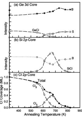
an-nealing to 680 K, the intensity of the GeCl component in the Ge 3d spectra 共Fig. 1兲 also decreases, as depicted in Fig. 4共a兲, and a second component 共labeled Cls) in the Cl 2 p spectra 共Fig. 3兲 arises at a binding energy 0.64 eV higher than for Clg. The normalized integrated intensities of the Clg
and Cls components in Fig. 3 account for the relative
abun-dance of surface Cl–Ge and Cl–Si species and are plotted in Fig. 4共c兲. The intensity of the total initial Cl coverage is about 1 ML, as suggested in Refs. 14 and 15.
As Fig. 4共c兲 depicts, the coverage of Cl gradually de-creases to only ⬃0.8 ML at around 550 K. Since Cl–Ge bonds are weak and the etch product GeCl2 desorbs at ⬃620 K on the Cl:Ge共100兲 surface,16
a small amount of Cl2
is likely to be recombinatively desorbed at this temperature range. The Cl coverage decreases more rapidly between 550 and 620 K in the form of Cl2 or GeCl2.
19
In Figs. 4共b兲 and 4共c兲, it is discernible that the intensity evolution of the SiCl component closely resembles that of the Cls component in
the Cl 2 p spectra, strongly implying that the formation of the Cl–Si bonds on the surface. Since Cl atoms can only form single bonds and they always terminate the surface. Thus, the formation of the Cl–Si bonds denotes the elimination of ex-isting Cl–Ge bonds, leading to the decrease in the intensity of the GeCl component, as shown in Fig. 4共a兲. This replace-ment of Cl–Si bonds with Cl–Ge bonds suggests that the deposited Si atoms, which have indiffused into the subsur-face region, must move upwards and undergo place ex-change with Ge atoms bonding with Cl. As shown in Fig. 4共c兲, about 0.5 ML of chlorine atoms remain on the surface at 680 K and mostly bond with Si. Above 680 K, the inten-sity of Cl 2 p declines more rapidly, as indicated by the re-FIG. 3. Cl 2 p core-level photoemission spectra共circles兲 for the
Cl-terminated Ge(100)-2⫻1, the 0.8-ML–Si/Ge(100)-2⫻1 sample and the same sample after annealing at various tempera-tures. Again, the relative binding energy refers to the corresponding Ge 3d5/2line of the B component in Fig. 1. The curves show the overall fits共solid curves兲 and their decomposition into the Clsand Clgcomponents.
FIG. 4. Intensities of the individual components derived from the共a兲 Ge 3d, 共b兲 Si 2p, and 共c兲 Cl 2p core-level spectra. The extra data points at 325 K共on the Y axis兲 mark the intensities of relevant components before Cl2exposure.
BRIEF REPORTS PHYSICAL REVIEW B 64 233302
duction in Cl 2 p intensity. After complete desorption of Cl at 820 K, the integrated intensity of Ge 3d remains almost unchanged while that of Si 2 p is ⬃33% lower than before Cl adsorption. This means that ⬃0.25 ML of the total 共0.8 ML兲 deposited Si atoms is removed from the sample. There-fore, the desorption product around 700 K is in the form of SiCl2. This desorption temperature is appreciably lower than
the SiCl2 desorption peak (⬃830 K) on the Cl:Si(100)-2
⫻1 samples, which is likely due to the fact that the surface
Cl–Si species are now bonded with the subsurface Ge and that Ge–Si bonds are weaker than that of Si–Si bonds.
For a monolayer Si deposited Ge(100)-2⫻1 surface, a theoretical study showed that the energy for a segregated structure, in which Si occupies the second layer while Ge–Ge dimers float to the surface, is 0.38 eV/dimer lower than that for the nonsegregated 共Si–Si dimer terminated兲 surface.7 Chlorine adsorption dramatically reverses the situ-ation: the Cl–Si–Si–Cl monochloride surface is energeti-cally favored over the Cl–Ge–Ge–Cl surface共with Si in the second layer兲 by 0.3 eV per dimer.8 Therefore, thermody-namic forces drive the replacement of the Cl–Ge bonds by Cl–Si, upon thermal activation. The occurrence of the Si–Ge place exchange on the Cl:Si/Ge共100兲 surface has been simi-larly observed during atomic hydrogen exposure on the Ge-covered Si共100兲 surface.20 To explain the kinetics of the place exchange between Ge and Si, the authors in Ref. 20 proposed a dimer-vacancy diffusion-assisted mechanism, in which the exchange only proceeds via missing dimer vacan-cies in unit of dimers. Upon 680-K annealing of the Cl-terminated 0.8-ML–Si/Ge共100兲 sample, Figs. 2, 4共b兲, and 4共c兲 show that only about 0.5 ML Si moves to surface to form Cl–Si bonds, whereas, the intensity of SiCl component
is 1.2 times that of the bulk component before annealing. If the simple layer attenuation model is with ⬃3.3 Å escape depth,17 the Si atoms average moves ⬃2 atomic layers up-ward to exchange with Ge. Therefore, the exchange mecha-nism 共in which the exchanged Si and Ge layers are next to each other兲 proposed in Ref. 20 is not applicable here and the atomic detail for the exchange of Cl–Ge and Cl–Si species is not clear at this point. Since both the surface Si and Ge intermixing on Si共100兲21 and Si indiffusion on Ge共100兲18 have been found to occur at near room temperature without the introduction of defects, the activation energies of these surface reactions appear much lower than intuitive expecta-tion.
In summary, the chemical-state resolved Ge 3d, Si 2 p, and Cl 2 p core-level spectra demonstrate that 0.8-ML depos-ited Si indiffuses about 2 atomic layers deep on Ge(100)-2
⫻1 and that the 0.8-ML–Si/Ge共100兲 surface has a fully
Ge-terminated structure. Cl adsorption reverses the Si indiffu-sion upon annealing. These results are in excellent agreement with recent theoretical findings that the energy for a segre-gated structure is lower than that of the nonsegresegre-gated Si–Si dimer terminated surface and that the Cl–Si–Si–Cl monochloride surface is energetically much more favorable than the Cl–Ge–Ge–Cl surface. Above 680 K, chlorine de-sorbs in the form of SiCl2, although the top layer of the
starting 0.8-ML–Si/Ge共100兲 surface consists of Ge–Ge dimers only.
The authors wish to thank the National Science Council, Taiwan for financially supporting this work under Contract No. NSC 90-2112-M009-016. The authors grateful acknowl-edge W.H. Hung, Y.W. Yang, and L.J. Lai for their assis-tance.
*Electronic mail: [email protected]
1See, for example, D. J. Paul, Adv. Mater. 11, 191 共1999兲, and
references therein.
2F. Liu, F. Wu, and M. G. Lagally, Chem. Rev. 97, 1045共1997兲,
and references therein.
3D.-S. Lin, T. Miller, and T.-C. Chiang, Phys. Rev. B 67, 2187
共1991兲.
4P. C. Kelires and J. Tersoff, Phys. Rev. Lett. 63, 1164共1989兲. 5
D.-S. Lin, T. Miller, and T.-C. Chiang, Phys. Rev. B 47, 6543
共1993兲.
6T. D. Durbin, D. A. Lapiano-Smith, F. R. McFeely, F. J. Himpsel,
and J. A. Yarmoff, Surf. Sci. 330, 147共1995兲.
7S. J. Jenkins and G. P. Srivastava, Phys. Rev. B 57, 8794共1998兲. 8M. C¸ akmak, S. C. A. Gay, and G. P. Srivastava, Surf. Sci.
454-456, 166共2000兲.
9K. Nakagawa, A. Nishida, Y. Kimura, and T. Shimada, J. Cryst.
Growth 150, 939共1994兲.
10W. Dondl, G. Hu¨tjering, W. Wegscheider, J. Wilhelm, R. Scho¨rer,
and G. Abstreiter, J. Cryst. Growth 127, 440共1993兲.
11S.-J. Kahng, Y. H. Ha, D. W. Moon, and Y. Kuk, Appl. Phys. Lett.
77, 981共2000兲.
12S. M. Sze, Semiconductor Devices, Physics and Technology
共Wiley, New York, 1985兲.
13For review, see H. N. Waltenburg and J. T. Yates, Jr., Chem. Rev.
95, 1589共1995兲.
14I. Lyubinetsky, Z. Dohnalek, W. J. Choyke, and J. T. Yates, Jr.,
Phys. Rev. B 58, 7950共1998兲.
15R. D. Schnell, F. J. Himpsel, A. Bogen, D. Rieger, and W.
Stein-mann, Phys. Rev. B 32, 8052共1985兲.
16S. M. Cohen, T. I. Hukka, Y. L. Yang, and M. P. D’Evlyn, Thin
Solid Films 225, 155共1993兲.
17
F. J. Himpsel, F. R. McFeely, J. F. Morar, A. Taleb-Ibrahimi, and J. A. Yarmoff, in Photoemission and Adsorption Spectroscopy of
Solids and Interfaces with Synchrotron Radiation, Proceedings of the International School of Physics ‘‘Enrico Fermi,’’ edited
by G. Scoles共North-Holland, New York, 1991兲, Course CVIII.
18D.-S. Lin, T. Miller, and T.-C. Chiang, Phys. Rev. B 45, 11 415
共1992兲.
19Our separated study in annealing the Cl-covered Ge/Si共100兲
sur-faces shows that the GeCl2desorption is minimal. The 0.3-ML
chlorine desorbed between 550 and 620 K can bring about 0.15-ML Ge desorption at most.
20E. Rudkevich, F. Liu, D. E. Savage, T. F. Kuech, L. McCaughan,
and M. G. Lagally, Phys. Rev. Lett. 81, 3467共1998兲.
21X. R. Qin, B. S. Swartzentruber, and M. G. Lagally, Phys. Rev.
Lett. 84, 4645共2000兲.
BRIEF REPORTS PHYSICAL REVIEW B 64 233302