國立交通大學
電信工程研究所
碩士論文
CPW 寬頻圓極化天線設計及單層基板雙頻
PIFA 設計
Design of a CPW-fed Circularly Polarized
Antenna and a Single-layer Planar Inverted-F
Antenna with Dual-band Operation
研究生:潘玠倫 (Chieh-Lun Pan)
指導教授:吳霖堃 博士 (Dr.
Lin-Kun Wu
)
CPW 寬頻圓極化天線設計及單層基板雙頻 PIFA 設計
Design of a CPW-fed Circularly Polarized Antenna and a Single-layer Planar Inverted-F Antenna with Dual-band Operation
研究生:潘玠倫 Student:Chieh Lun Pan 指導教授:吳霖堃 博士 Advisor:Dr. Lin-Kun Wu
國立交通大學 電信工程研究所
碩士論文
A Thesis
Submitted to Institute of Communication Engineering College of Electrical and Computer Enginerring
National Chiao Tung University In Partial Fulfillment of Requirements
For the Degree of Master of Science
In Communication Engineering
June 2013
Hsinchu, Taiwan, Republic of China
i
CPW 寬頻圓極化天線設計及其非對稱接地面影響之
探討及
單層基板雙頻 PIFA 設計及其設計類型之探討
研究生:潘玠倫 指導教授:吳霖堃 博士 國立交通大學電信工程研究所碩士班 中文摘要 本篇論文由兩個主題性的探討所組成:一是探討CPW結構非對稱的接地面對 圓極化天線特性的影響,另一主題探討兩種天線類型所設計出的PIFA其特性上的 差異,並擇優者完成設計。 針對第一個主題,我們選擇CPW結構的圓極化天線由於其擁有較寬頻軸比的 優勢,先利用連接於接地面上L形狀的寄生金屬元件和直線的天線主體耦合,使 整體電流於遠場等效出兩個相位差90度、大小相同且互相垂直的電場向量,產生 圓極化的雛型,再藉由不對稱地截掉方形接地面的截角,有效的將軸比頻寬加大, 使其包括了兩個GPS應用頻帶(L1和L3),90%以上的天線輻射效率使得天線於兩 使用頻帶中,正 z 軸右手圓極化增益可達4 dB以上,本論文將會利用全波模擬軟 體(HFSS)呈現不同類型的非對稱接地面對於此天線圓極化軸比的影響,並將天線 研究結果實作並且量測其特性。 另一個主題是探討針對設計一個單層微小化雙頻帶 PIFA 較佳的天線類型。 我們以沒有多餘空間增加空氣介質為前提,分別利用 patch 天線和 monopole 天線 為雛型設計一個 PIFA,比較其尺寸、匹配頻寬、輻射效率、天線增益。由於 monopoleii
雛形的 PIFA 擁有高達 88%的輻射效率因此較適合用於設計此限制前提的 PIFA。 本論文將會利用全波模擬軟體分別模擬出兩個類型的天線設計特性並進行比較, 此外我們實作出以 monopole 為雛形的 PIFA 並量測其特性。
iii
Design of a CPW-fed Circularly Polarized Antenna with Asymmetrical Ground Discussion and
Design of a Single-layer Planar Inverted-F Antenna with Dual-band Operation and Designing type discussion
Student: Chieh-Lun Pan Advisor: Dr. Lin-Kun Wu
Institute of Communication Engineering College of Electrical and Computer Engineering
National Chiao Tung University
Abstract
This paper composed by two research topics. One is the effects of asymmetrical ground on CPW-fed wideband circularly polarized antenna for application of the GPS band and another is the effects of different antenna type on the design of single layer miniaturized dual-band planar inverted-F antenna
For the first topic, we choose the CPW-fed for the structure of the circularly polarized antenna due to the advantage that having wider axial ratio bandwidth than microstrip-fed. We generate the circularly polarized feature which means that there are two orthogonal resonant modes with equal amplitude and 90 phase difference by using an L-shape strip connecting on the ground of CPW structure coupling to the striate main radiator. By truncating two angles on the opposite position of the ground the axial ratio bandwidth can be broaden obviously so that the application of the proposed antenna can include two bands (L1 and L3) of the GPS application. The high radiation efficiency above 90 % both for two operating band makes the RHCP gain on
iv
the +z axial higher than 4 dB. In this paper we will illustrate the different axial ratio feature caused by different kind of asymmetrical ground by using the 3D full wave simulator (HFSS) and the measured research result will also be shown.
In another topic, we will discuss and investigate a better antenna type for designing a single layer miniaturized dual-band PIFA. We use a patch antenna and a monopole antenna for the two PIFA designing bases with a restriction that we don’t have additional space for an air layer. After comprehensive comparing the monopole based PIFA is chosen due to its high radiation efficiency above 88 %. We will show and compare the two simulated antenna design by the HFSS, furthermore the monopole based PIFA will be fabricated and measured.
v 誌謝 我能夠順利完成碩士論文以及取得碩士學位,首先最要感謝吳霖堃教授和周 復芳教授,謝謝教授們提供了這樣自由的研究環境以及充足資源,讓我對天線的 設計有一定的了解、實作的過程有很紮實的經驗。另外也感謝口試委員王健仁老 師在碩論上細心的指正以及建議,使碩論更加完善。 感謝舜哥對我在網路分析儀校正、散射參數的量測及天線遠場量測上大力的 指導和協助,並且灌輸我嚴謹的想法、態度和提供許多相關書籍、參考文獻。 感謝 Double 和卡爺在每周的 meeting 了解我研究上的問題並提出建議以及替 我注意研究的進度。 感謝易懋教我使用碩士班研究中最重要核心的模擬軟體(HFSS)以及給予我圓 極化天線的設計上非常多的建議。 感謝張雨翔 : 碩士班兩年的同窗,當初只有你認同我餐廳內用的堅持;打球、 重訓、外出吃飯都會找我,研究室許許多多的休閒活動也大多是你主辦提議,這 讓我的研究室生活也有歡樂愜意的時候。 感謝林學群,在你轉到周老師研究室的同時也剛好成為了我的鄰居,在你身 上我看到另一種和同儕、學長相處的親切感,也因為你的加入讓我的碩二生活多 了一個可以討論研究、談天說地的朋友。 感謝電路組的阿秀、MOMO、馮盛、八妹,實驗室的出遊你們都熱情的參與, 也會提出許多令人興奮的建議和行程,雖然我們的研究方向不同,但因為這些規 劃出遊和聚餐的經驗,讓我們彼此更熟識了解。 感謝研究室的學弟妹,每天都一起認真的做研究到晚上,讓我在晚上研究疲 勞的時候也有人可以聊天說笑,轉換一下心情。 最後感謝我的家人和女朋友阿毛,若沒有你們的支持和督促我絕對無法順利 地拿到碩士學位,爸媽你們總是耐心地叮嚀在練舞和研究間要衡量取捨,阿毛妳 總會給我許多綜觀且實用的建議,即使妳並不懂那些艱澀的內容。未來,我會牢 記在碩士班所學到的專業和態度來幫助我的人生繼續向前,萬分感激不盡!
vi
Table of the Contents
中文摘要...I Abstract...III 誌謝...V TABLE OF CONTENTS...VI LIST OF FIGURES...VIII LIST OF TABLES ...XI
CHAPTER 1:Introduction ... 1
1.1 Introduction of Wideband CPW-fed Circularly Polarized Antenna ... 1
1.2 Introduction of Single Layer Dual-band Planar Inverted-F Antenna ... 2
CHAPTER 2:Design of a CPW-fed Circularly Polarized Antenna with Asymmetrical Ground Discussion ... 4
2.1 Basic Theory ... 4
2.1.1 Theory of Polarization ... 4
2.2 The Effects of Asymmetrical Ground on Performances of the CP Antenna ... 9
2.2.1 The Structure for a Prototype of CP Antenna for GPS Application ... 9
2.2.2 Discussion of Structure Parameters ... 11
2.2.3 The Effects of Different Asymmetrical Ground ... 16
2.3 Simulation and Measured Result ... 23
2.4 Conclusion ... 27
CHAPTER 3:Design of a Single-layer Planar Inverted-F Antenna with Dual-band Operation and Designing type discussion ... 28
vii
3.1.1 Size Reduction Technique of Patch Antennas ... 29
3.1.2 Tuning the Resonant Frequency of Patch Antennas by Using Shorting Pins ... 32
3.2 Two Designs of Dual-Band Planar Inverted-F Antenna with Single Layer for GSM and DCS Application ... 33
3.2.1 The Two Geometries of the Dual-Band PIFA ... 34
3.2.2 Investigating Parameters of Controlling Each Frequencies for the Two Kinds of PIFA ... 42
3.3 Simulation and Measured Result ... 51
3.4 Conclusion ... 57
viii
List of Figures
Figure 2.1 (a) Rotation of a plane electromagnetic wave and (b) its polarization ellipse
at z = 0 as a function of time. ... 6
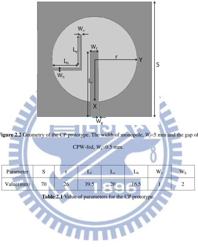
Figure 2.2 Geometry of the CP prototype. The width of monopole, Wf=5mm and the gap of CPW-fed, Wg=0.5mm. ... 10
Figure 2.3 The distribution of surface current on the ground and the monopole at 1381 MHz ... 11
Figure 2.4 The variation when L-shape strip moving down (a) S11 and (b) axial ratio. ... 12
Figure 2.5 The variation as Lh changing (a) S11 (b) axial ratio. ... 14
Figure 2.6 The variation as Lv changing (a) S11 (b) axial ratio. ... 15
Figure 2.7 The geometry of proposed antenna. ... 16
Figure 2.8 The variation as Lu changing (a) S11 and (b) axial ratio. ... 18
Figure 2.9 The variation as Ll changing (a) S11 and (b) axial ratio. ... 19
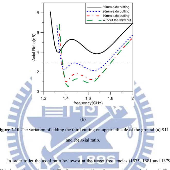
Figure 2.10 The variation of adding the third cutting on upper left side of the ground (a) S11 and (b) axial ratio. ... 21
Figure 2.11 The distribution of electric field on the +z axial surface of proposed antenna at 1575 MHz (a) source phase 0 (b) source phase 90 . ... 22
Figure 2.12 The simulation and the measurement result of the (a) return loss and (b) axial ... 24
Figure 2.13 The simulated radiated power at +z axis above the antenna. ... 25
Figure 2.14 The measurement result of RHCP and LHCP radiation pattern on yz cut at (a) 1381 MHz and (b) 1575 MHz. ... 26
Figure 2.15 The photograph of the fabricated antenna ... 26 Figure 3.1 Electric field distributions of half-wave patch and shorted quarter-wave
ix
patch. ... 30
Figure 3.2 Geometry of partially shorted patch. ... 30
Figure 3.3 Size reduction by using inverted-F patch.. ... 31
Figure 3.4 Rectangular patch with shorting pin. ... 31
Figure 3.5 A rectangular patch with two shorting pins. ... 32
Figure 3.6 The prototype of the PIFA for the GSM900 application.. ... 35
Figure 3.7 The variation of the return loss as the shorting pin moves. ... 35
Figure 3.8 The variation of input matching as the feeding move along the right edge 36 Figure 3.9 The geometry of prototype embedded by a slot for the DCS band. ... 37
Figure 3.10 The variation of the return loss as the value of Lp changes. ... 37
Figure 3.11 The variation of the input matching as the feed moves. ... 38
Figure 3.12 The prototype of the monopole based PIFA operating for GSM900 band 39 Figure 3.13 The variation of the resonant frequency when value of Lm changes ... 39
Figure 3.14 The variation of the impedance matching when the via moves ... 40
Figure 3.15 The geometry of the monopole antenna embedded by an L-shape Slot for DCS1800 band ... 41
Figure 3.16 The variation of the DCS band as the value of Ls changes ... 41
Figure 3.17 The proposed patch based antenna for GSM and DCS bands ... 43
Figure 3.18 The simulated return loss of the proposed patch based PIFA ... 43
Figure 3.19 The distribution of the surface current on the radiator at (a) 0.9 GHz (b) 1.8GHz ... 44
Figure 3.20 The simulated radiation efficiencies of the patch based PIFA by HFSS ... 44
Figure 3.21 The distribution of the electric field in the substrate at (a) 0.9 GHz (b) 1.8GHz ... 45
Figure 3.22 The proposed monopole based antenna for GSM and DCS bands ... 46
x
Figure 3.24 The distribution of the surface current on the metallic radiator at (a) 0.95
GHz (b) 1.75 GHz ... 48
Figure 3.25 The simulated radiation efficiencies of the patch and monopole based
PIFA by HFSS ... 50
Figure 3.26 The simulated and measured return loss of the proposed monopole based
PIFA ... 51
Figure 3.27 The measured radiation pattern of Eθ on xz plane at (a) 0.95 GHz and (b)
1.8 GHz ... 52
Figure 3.28 The measured radiation pattern of Eφ on xz plane at (a) 0.95 GHz and (b)
1.8 GHz ... 53
Figure 3.29 The measured radiation pattern of Eθ on yz plane at (a) 0.95 GHz and (b)
1.8 GHz ... 54
Figure 3.30 The measured radiation pattern of Eφ on yz plane at (a) 0.95 GHz and (b)
1.8 GHz ... 55
Figure 3.31 The (a) front side and (b) back side photograph of the fabricated antenna
xi
List of Tables
Table 2.1 Value of parameters for the CP prototype. ... 10
Table 2.2 Value of parameters for the proposed antenna. ... 16
Table 3.2 The value of parameters for the proposed patch based PIFA.. ... 43
1
CHAPTER 1:Introduction
1.1 Introduction of Wideband CPW-fed Circularly Polarized Antenna
In the modern development of communications, many introductions of high speed communication technologies show that reducing the loss caused by the misalignment between antennas is very important. Therefore, circularly polarized (CP) antennas become more and more popular for communication systems which are sensitive to the variations of weather and atmosphere such as radar tracking, satellite communication, navigation and radio frequency identification (RFID) due to its better mobility and flexibility of orientation angle and reduction of multipath reflections for transmitting and receiving.
The way of generating circular polarization is exciting two near-degenerated orthogonal resonated modes with equal amplitude and 900 phase difference. Several techniques that are usually used to design CP antennas are embedding L-shape grounded strips or slots [1, 2], using asymmetrical ground or feeding [3-5], and embedding circular-shape strips or plates and some design even use spiral [6-9]. Furthermore a special design is making a strip on the ground of CPW structure orthogonal to the main radiator [10-13]. To achieve the wider axial ratio bandwidth, a coplanar waveguide (CPW) feeding is chosen rather than a microstrip feeding which is usually used for many single-fed CP antennas [14].
Circular polarization is commonly adopted in global positioning system (GPS) and other satellite communications; in general the major GPS receivers only operate at L1 band (1575.42 MHz) with right hand circular polarization. However, for more applications such as military using and nuclear detonation detection, some CP antennas for GPS are designed covering L1, L2 (1227 MHz) and L3 (1381 MHz) band.
2
1.2 Introduction of Single Layer Dual-band Planar Inverted-F Antenna
It has become more and more popular even a requirement to design multiband antennas for the current personal wireless communications that are required to support so many different communication standards and services around the world. To satisfy these modern communication devices, the antennas should be able to operate at as many frequency bands as possible with acceptable return loss and other radiation performances. Besides the multiband performances, the antennas installed in portable handheld wireless communication devices should have the feature of compact, low-profile, tough, light weight, and easily manufacturing.
The planar inverted-F antenna (PIFA) is a very appropriate candidate for portable wireless devices because of its compactness and the features stated above. Recently, several multi-frequency antennas arising from the PIFA have been presented. For triple or more frequency operation, there are many methods can realize this performance. Some designs [15, 16] are realized using parasitic elements for exciting more resonant bands. Some designs [17-20] use embedded slots in the radiating element or the ground to generate some additional bands which are around the main resonant frequency for increasing number of band or enhancing the bandwidth of the main resonant frequency. Furthermore, there are some designs [21] can achieve triple operating bands using only two shorting pins and one feeding. However these designs of the reference are all using thick air substrate between the radiator and the ground so that the volume of these antennas is too huge for using an internal antenna of modern portable communication devices.
The antenna design is always determined by the dimension of the PCB (Printed Circuit Board), which is limited by the size of the handset or wireless device [22]. The antenna height is especially an important limitation so it should be small enough to satisfy the size of new generation, ultra-slim cellular phones, as the result we have to set this kind of size restriction to our research specification when it comes to having no more space for an air substrate.
3
The proposed miniaturized dual-band PIFA was fabricated on a FR4 board of single substrate with the industrial required size (40 mm x 100 mm), and it can be used for the application of GSM900 (880-960 MHz) and DCS1800 (1710-1880 MHz).
4
CHAPTER 2:Design of a CPW-fed Circularly Polarized
Antenna with Asymmetrical Ground Discussion
In this chapter, a wideband CP antenna with coplanar waveguide (CPW) feeding operating on GPS band (1381 and 1575 MHz) is presented here. We use the feeding way of CPW network, because of the wider axial ratio bandwidth compared to the performance of microstrip feeding. The proposed antenna has the features of low cost and easily manufacturing due to the single layer of CPW structure so that it is suitable to current GPS and satellite communication devices. The used simulator is 3D full-wave EM solver, Ansoft HFSS, and we will show simulated and measured result of this design. The discussion of effects caused by changing the shape of asymmetrical ground will be processed by simulations.
2.1 Basic Theory
In this section, we will introduce some essential theories which are always used for designing circularly polarized antennas as references from “Antenna Theory analysis and design” Third Edition authored by Constantine A. Balanis. [23]
2.1.1 Theory of Polarization
Polarization of a radiated wave is defined as “that property of an electromagnetic wave describing the time-varying direction and relative magnitude of the electric-field vector; specifically, the figure traced as a function of time by the extremity of the vector at a fixed location in space, and the sense in which it is traced, as observed along the direction of propagation.” Polarization then is the curve traced by the end point of the arrow (vector) representing the instantaneous electric field. The field must be observed along the direction of propagation. A typical trace as a function of time is shown in Fig. 2.1 (a) and (b). If the vector
5
that describes the electric field at a point in space as a function of time is always directed along a line, the field is said to be linearly polarized. In general, however, the figure that the electric field traces is an ellipse, and the field is said to be elliptically polarized. Linear and circular polarizations are special cases of elliptical, and they can be obtained when the ellipse becomes a straight line or a circle, respectively.
6
(b) Polarization ellipse
Figure 2.1 (a) Rotation of a plane electromagnetic wave and (b) its polarization ellipse at z =
0 as a function of time.
The instantaneous field of a plane wave, traveling in the negative z direction, can be written as
E(z; t) =
̂E
x(z; t) +
̂E
y(z; t)
(1)The instantaneous components are related to their complex counterparts by
E
x(z; t) = Re[E
x−e
j(ωt+kz)] = Re[E
xoe
j(ωt+kz+φx )]
= E
xocos(ω
t+ k
z+ φ
x)
(2)E
y(z; t) = Re[E
y−e
j(ωt+kz)] = Re[E
yoe
j(ωt+kz+φy )]
= E
yocos(ω
t+ k
z+ φ
y)
(3)7
(A) Linear Polarization
For the wave to have linear polarization, the time-phase difference between the two components must be
Δφ = φ
y− φ
x= nπ, n = 0, 1, 2, 3, . . .
(4)(B) Circular Polarization
Circular polarization can be achieved only when the magnitudes of the two components are the same and the time-phase difference between them is odd multiples of π/2. That is,
|E
x| = |E
y|→E
xo= E
yo (5)Δφ = φ
y− φ
x=
(
+ 2n)π, n = 0, 1, 2, . . .
(6)Positive for left hand CP and negative for right hand CP. If the direction of wave propagation is reversed (+z direction), the phases for LHCP and RHCP rotation must be interchanged.
(C) Elliptical Polarization
Elliptical polarization can be attained only when the time-phase difference between
the two components is odd multiples of π/2 and their magnitudes are not the same or when the time-phase difference between the two components is not equal to multiples of π/2
(irrespective of their magnitudes). That is,
|E
x|
|E
y|→E
xoE
yo (7)Δφ = φ
y− φ
x=
(
+ 2n)π, n = 0, 1, 2, . . .
(8)or
Δφ = φ
y− φ
x, n = 0, 1, 2, . . .
(9)For elliptical polarization, the curve traced at a given position as a function of time is, in general, a tilted ellipse, as shown in Fig 2.1(b). The ratio of the major axis to the minor axis is referred to as the axial ratio (AR), and it is equal to
AR
8
In conclusions,
(A) Linear polarization:( → )
Single-axial or bi-axial with in phase or 180 out of phase
(B) Elliptical Polarization:( ≥ 0 dB)
Bi-axial with quadrature phase
(C) Circular Polarization:( 0 dB)
Bi-axial with identical magnitude and quadrature phase
9
2.2 The Effects of Asymmetrical Ground on Performances of the CP Antenna
In this section, a wideband circularly polarized monopole antenna with a CPW-fed is proposed. The L-shape strip which connecting with the ground etched by a circle mainly contributes the feature of right-hand circular polarization (RHCP). Additionally by adding the pair of unequal truncates on opposite position of the ground, the bandwidth of axial ratio can be broaden. Fig. 2.7 shows the configuration of the proposed antenna. The antenna is fabricated on an FR4 substrate of 1.6 mm thickness with a dielectric constant of 4.4 and a loss tangent of 0.02. The 10 dB return loss impedance bandwidths are 9.6 %( 1.16-1.28 GHz) and 19.5 %( 1.34-1.64 GHz), and the 3 dB axial-ratio bandwidth is 28.69 %( 1.36-1.82 GHz). Moreover, we will investigate many cases of the prototype with different asymmetrical ground by using 3D full wave simulator, HFSS. Finally, experimental results will show the proposed antenna having good return loss and circular polarization characteristics.
2.2.1 The Structure for a Prototype of CP Antenna for GPS Application
The geometry of a circularly polarized antenna was shown as Fig. 2.2. It consists of a straight-line radiator, a coplanar rectangular ground with a circle etching in. The radius of the circle etching in the ground is r, and the straight radiator of width Wf and length Lf with the
gap of feed line, Wg. The length of vertical strip, Lv and the length of horizontal strip, Lh
compose the L-shape strip which is applied to generate resonator for exciting two orthogonal modes with equal amplitude and 90 phase difference. The antenna is fabricated on an FR4 substrate of size 70 mm × 70 mm with a dielectric constant of 4.4 and a loss tangent of 0.02. The thickness of the substrate is 1.6 mm. The width of feeding line is Wf=5 mm and Wg=0.5
mm for a CPW input impedance of 50 Ohm. The optimized parameters of the prototype for circularly polarized antenna are listed in Table 2.1
10
Figure 2.2 Geometry of the CP prototype. The width of monopole, Wf=5 mm and the gap of
CPW-fed, Wg=0.5 mm.
Parameter S r Lf Lv Lh Wv Wh
Value(mm) 70 26 39.5 20 16.5 1 2
11
2.2.2 Discussion of Structure Parameters
This section will discuss the variations to the return loss and axial ratio, when the length and position of L-shape strip was changed, and the axial ratio of the prototype will be optimized closing to the application L3, L4 (1381 MHz, 1379.9 MHz) of GPS band.
I. Changing the position of L-shape strip
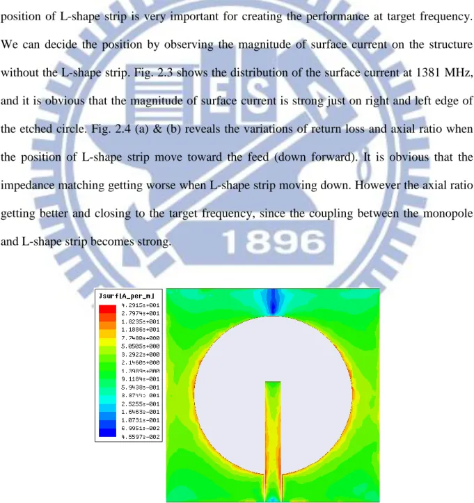
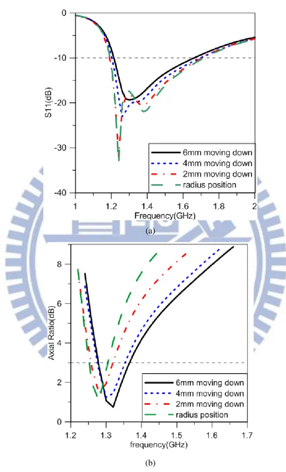
Because the circularly polarized characteristic is mainly created by L-shape strip, the position of L-shape strip is very important for creating the performance at target frequency. We can decide the position by observing the magnitude of surface current on the structure without the L-shape strip. Fig. 2.3 shows the distribution of the surface current at 1381 MHz, and it is obvious that the magnitude of surface current is strong just on right and left edge of the etched circle. Fig. 2.4 (a) & (b) reveals the variations of return loss and axial ratio when the position of L-shape strip move toward the feed (down forward). It is obvious that the impedance matching getting worse when L-shape strip moving down. However the axial ratio getting better and closing to the target frequency, since the coupling between the monopole and L-shape strip becomes strong.
12
(a)
(b)
13
II. Changing the length of Lv and Lh
We already know that the coupling between L-shape strip and the monopole is a critical point when we want to control the performance of impedance matching and axial ratio. The distance between these two elements, Lh and the vertical length of L-shape, Lv
should be discussed and optimized.
From Fig. 2.5 (a) & (b) we can know that impedance matching become worse as Lh
increasing. The coupling is becoming strong due to the distance between L-shape strip and the monopole. Furthermore if we want to have a good axial ratio performance, the value of
Lh should be controlled in a range between 15~17 mm for having an proper coupling. On the other hand, the variation of S11 and axial ratio as Lv changing is shown in Fig. 2.6 (a) &
(b). It can be observed that when the length of vertical strip increases, the return loss become better, and the axial ratio becomes leaving the target frequency and getting worse. The Lv can also contribute an effect to S11 and axial ratio, because the quantity of coupling
is also depending on the current density on the vertical strip.
In order to maintain both good return loss and axial ratio, the position of L-shape strip, and the values of Lh, Lv must be traded off. The structure of prototype for fine-tuned edition
14
(a)
(b)
15
(a)
(b)
16
2.2.3 The Effects of Different Asymmetrical Ground
The concept of cutting a pair of truncates on the ground is come up with from the textbook; a circularly polarized patch antenna can be create by cutting off a pair of angles on opposite corners. In this section we are curious about whether cutting truncates on the corner of rectangular ground can improve the performance of axial ratio or not. The lengths of two unequal-size isosceles truncates cut on two opposite corners of the rectangular ground are Lu
and Ll, and they enhance the axial ratio bandwidth for covering triple GPS applications.
Moreover, changing the magnitude of the length of upper and lower isosceles truncates unequally can control the position and bandwidth of the axial ratio. The geometry of proposed antenna is shown in Fig. 2.7, and values of parameters are listed in Table 2.2.
Several kinds of asymmetrical ground will be investigated in following parts, and the variation of parameters will also be discussed.
Figure 2.7 The geometry of proposed antenna.
Parameters S r Lf Lv Lh Wv Wh Lu Ll
Value(mm) 70 26 39.5 20 16.5 1 2 30 20
17
I. Truncating only one angle on upper right of the ground
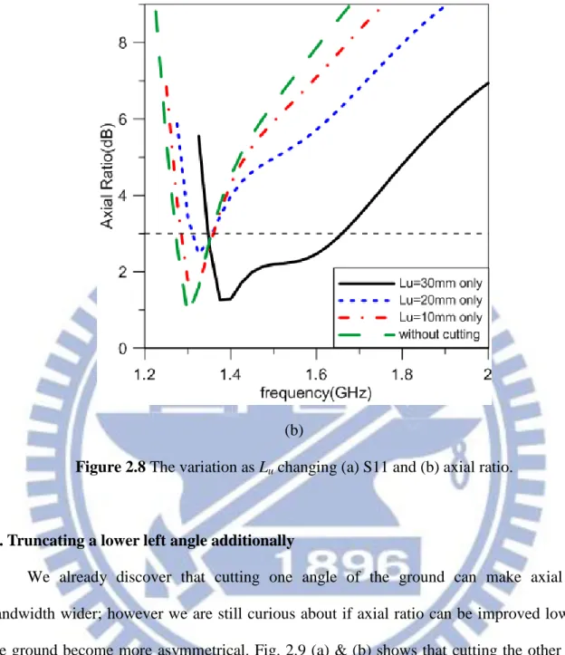
Some former investigations has indicated that asymmetrical ground of CPW structure can provide wide axial ratio bandwidth. For our case it is obvious that the bandwidth of axial ratio was greatly broaden in Fig. 2.8 (b) when the level of truncating (Lu) increasing.
Although the return loss is spoilt in Fig. 2.8 (a), it still can cover L1, L3 and L4 band of GPS as the value of Lu becomes 30mm, and it is noted that truncating the corner will cause the mode splitting.
18
(b)
Figure 2.8 The variation as Lu changing (a) S11 and (b) axial ratio.
II. Truncating a lower left angle additionally
We already discover that cutting one angle of the ground can make axial ratio bandwidth wider; however we are still curious about if axial ratio can be improved lower as the ground become more asymmetrical. Fig. 2.9 (a) & (b) shows that cutting the other angle off on the opposite position additionally indeed make axial ratio lower than having only upper right truncating, furthermore it causes few effects to the return loss for the target frequency bands.
19
(a)
(b)
20
III. Truncating the third angle on upper left side of the ground
After adding the second truncating the antenna has been designed for the application of GPS on L1, L3 and L4 (1575, 1381 and 1379 MHz) band successfully. In order to conform whether there is a better case can be created by other kind of asymmetrical ground or not, we still discuss the case of the ground with the third truncating on the upper left side. Fig. 2.10 (a) & (b) depicts the performance of the antenna varying as the level of the truncating on upper left side increasing. It is clear that the axial ratio gets worse very severely as soon as the third truncating is added. The return loss at L1 band (1575 MHz) of GPS is also spoiled when the cutting level becomes too much.
21
(b)
Figure 2.10 The variation of adding the third cutting on upper left side of the ground (a) S11
and (b) axial ratio.
In order to let the axial ratio be lowest at the target frequencies (1575, 1381 and 1379 MHz), Lu and Ll must be tuned. The fine-tuned edition of proposed antenna is shown in Fig.
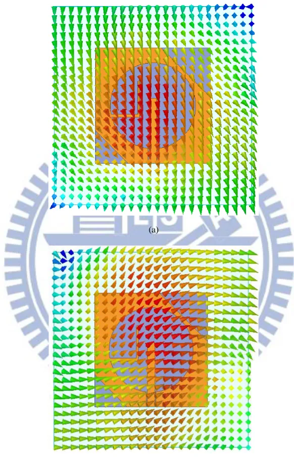
2.7, and the value of parameters is depicted in Table 2.2. Fig. 2.11 (a) & (b) shows the distribution of electric field with phase 0 degree and 90 degree on the +z axial surface of radiation box at L1 band (1575 MHz). It is obvious that these two electric-field directions of phase 0 and phase 90 degree are orthogonal; furthermore it is right hand circular polarization (RHCP).
22
(a)
(b)
Figure 2.11 The distribution of electric field on the +z axial surface of proposed antenna at
23
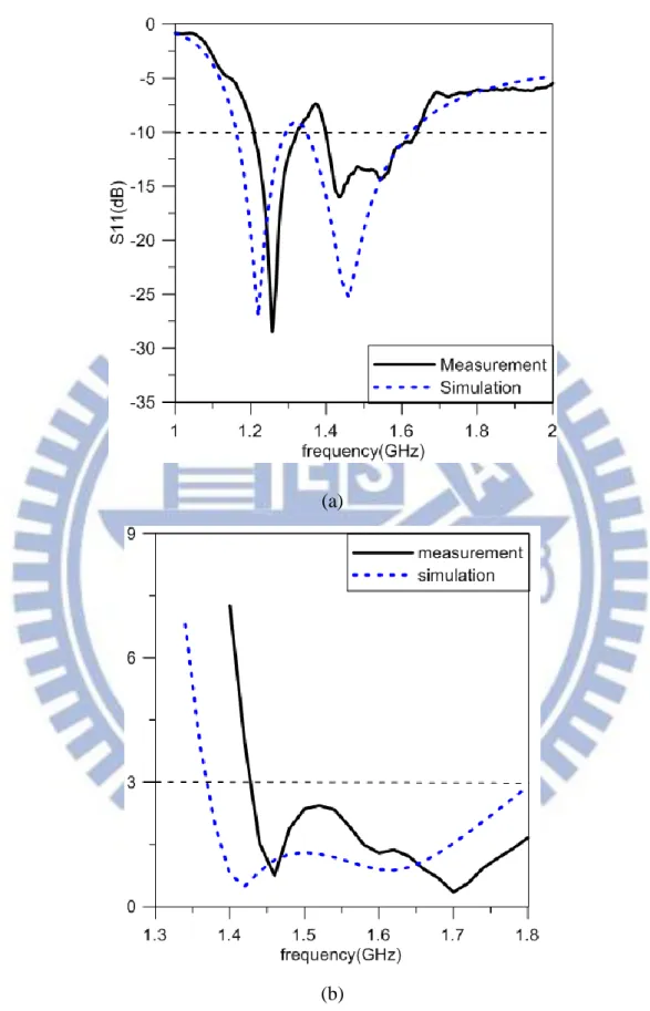
2.3 Simulation and Measured Result
The simulation and the measured result of the return loss are shown in the Fig. 2.12 (a), and the result of axial ratio is shown in the Fig. 2.12 (b). The 10dB impedance matching bandwidth of the operating frequency is about 15.8 % (1.4-1.64 GHz). Due to the frequency shifting the L3 band (1381 MHz) can’t reach the level of 10 dB impedance matching but it is still in accordance with the commercial specification of 6 dB return loss below. The bandwidth of 3 dB axial ratio is 28.4 % (1.42-1.89 GHz) and the axial ratio at 1381 MHz and 1575 MHz are 10.35 dB and 1.58 dB respectively. Although the frequency shifting let the proposed axial ratio can’t include the L3 band of GPS application, the most major using, L1 band of GPS application, is in the specification.
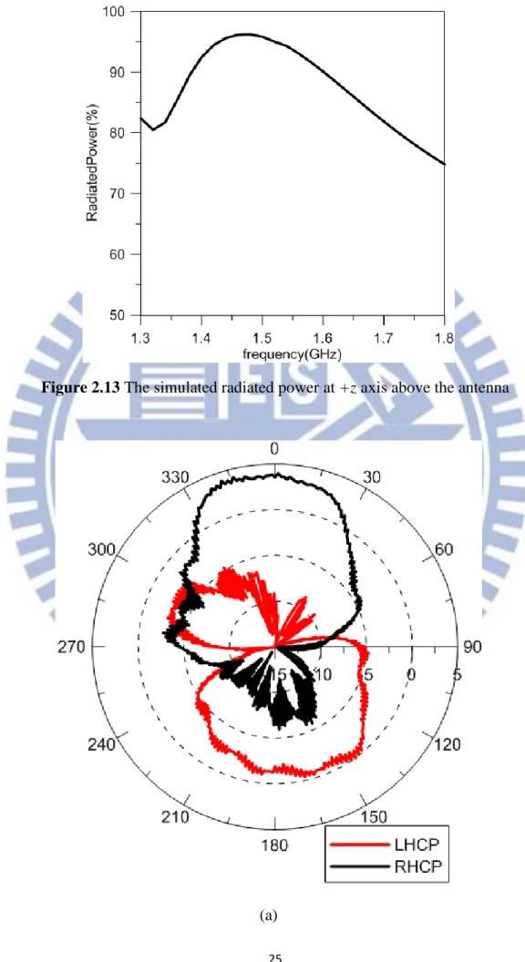
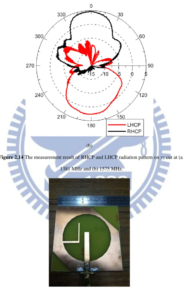
The radiated power above the antenna at the position of +z axis calculated by the simulator, HFSS, is shown in Fig. 2.13 and the measured radiation patterns of RHCP and LHCP on the cut of YZ plane at 1381 MHz and 1575 MHz are shown in Fig. 2.14 (a) & (b). The RHCP gain on the direction of +z axis is about 3.9 dBi at 1381 MHz and 4.6 dBi at 1575 MHz; additionally the LHCP gain on the direction of –z axis is about -1.9 dBi at 1381 MHz and 2.6 dBi at 1575 MHz. Finally the photograph of the realistic fabricated antenna is shown in Fig.2.15.
24
(a)
(b)
Figure 2.12 The simulation and the measurement result of the (a) return loss and (b) axial
25
Figure 2.13 The simulated radiated power at +z axis above the antenna
26
(b)
Figure 2.14 The measurement result of RHCP and LHCP radiation pattern on yz cut at (a)
1381 MHz and (b) 1575 MHz.
27
2.4 Conclusion
A CPW-fed wideband circularly polarized antenna for the application on L3 and L1 (1381 MHz and 1575 MHz) of GPS band is proposed. The feature of circular polarization is created by an L-shape strip connecting on the inner edge of the CPW ground and is enhanced by using an investigated asymmetrical ground. Thanks to the asymmetrical ground the application of the proposed antenna can be promoted. The realized bandwidth of return loss and axial ratio are 15.8 % (1.4-1.64 GHz) and 28.4 % (1.42-1.89 GHz) respectively. The RHCP gain on the +z axial for the L3 and L1 of GPS band is 3.9 dBi and 4.6 dBi and the radiated power is above 90 % both for the two operating bands. The proposed antenna is suitable for the modern portable communication devices and satellite satellitic systems due to its advantages of broadband, low cost and easy manufacturing.
28
CHAPTER 3:Design of a Single-layer Planar Inverted-F
Antenna with Dual-band Operation and Designing type
discussion
In recent time requires for small size and simple geometry antennas especially for compact mobile phone and portable devices are developed fast. As the result internal antennas are very popular choices compared to the conventional external antennas. When using the concept of microstrip patch antennas, the patch element size should be reduced as the size of ground plane is restricted by the modern communicating devices.
The planar inverted-F antenna (PIFA) have become the most attractive candidate for mobile handsets due to its desirable advantages such as high efficiency multi-frequency operating, moderate bandwidth, low profile, low cost and lower power absorption for user compared with conventional external antennas.
In Chapter 3 we will design a dual-band PIFA which was fabricated on a FR4 board of single substrate with the industrial required size (40 mm x 100 mm), and we will investigate the miniaturized PIFA by using two basic antenna types for the PIFA structure in order to get a trade-off between the operating bandwidth, antenna efficiency and the antenna size. The proposed antenna can be used for the application of GSM900 (880-960 MHz), DCS1800 (1710-1880 MHz).
3.1 Basic Theory
In this section, we will introduce some essential theories which are always used for designing planar inverted-F antennas as references from “Microstrip Patch Antennas” authored by Kai Fong Lee and Kwai Man Luk. [24]
29
3.1.1 Size Reduction Technique of Patch Antennas (A) Quarter Wave Patch of Using Shorting Wall
The electric field distributions under the patch for the TM01 and TM10 modes have a null along the center of the patch. The fields are not perturbed when a short is placed at the null line, as shown in Fig. 3.1. This results in a shorted quarter-wave patch, with the same resonant frequency as the regular half-wave patch. The area will be half-wave patch if the dimension along x remains the same. If the dimension along x is reduced by half (from a to a/2) so that the aspect ratio remains the same as the original patch, the area will be four times smaller.
(B) Partially Shorted Patch and Planar Inverted F Antenna
Fig. 3.2 shows the geometry in which the shorting wall, instead of extending fully across the width of the patch a, has a width s, where s a. When s/a decrease, the resonant frequency will decrease and it represent the reduction of the antenna size. The partially shorted patch in the form shown in Fig. 3.3 is known as the planar inverted F antenna (PIFA), because the side view looks like an inverted F. The width of the shorting wall w is approximately 0.2L1 while the dimensions of L1 and L2 are on the order of 1/8λ0.
(C) Use of Shorting Pin
Another technique for reducing the patch size, very similar to the inverted-F method, is to use a shorting pin. This is illustrated in Fig. 3.4. The shorting pin causes the fields underneath the patch to bounce back-and-forth. The field starts to radiate once the bouncing distance reaches half-wavelength. As a result of the multiple bounce, the physical size of the patch is reduced. Since the bounces are non-unidirectional, the fields can radiate out from almost all edges of the patch, resulting in high cross-polarization. However, for certain applications such as cellular phone communication in a multi-path environment, high- cross polarized fields are not a concern.
30
coupled to the pin. This is equivalent to increasing the permittivity of the substrate, which further contributes to reduction in frequency or size of the patch (measured in wavelength), and it should be mentioned that the bandwidth can be improved by using multiple shorting pins.
Figure 3.1 Electric field distributions of half-wave patch and shorted quarter-wave patch.
31
Figure 3.3 Size reduction by using inverted-F patch.
32
3.1.2 Tuning the Resonant Frequency of Patch Antennas by Using Shorting Pins
The value of εr can also be changed by introducing shorting pins at various points
between the patch and the ground plane. These shorting pins present an inductance, and therefore affect the effective permittivity of the substrate. For example, a rectangular patch antenna with two shorting pins is shown in Fig. 3.5, and the resonant frequency is dependent on the separation of the two pins. When the distance between two pins is decreasing, the resonant frequency can be moved toward lower frequency.
33
3.2 Two Designs of Dual-Band Planar Inverted-F Antenna with Single Layer for GSM and DCS Application
In this section, a dual-band planar inverted-F antenna will be designed by two kinds of antenna for the basic PIFA structure. We use patch antenna and the monopole antenna as the basic structure of the proposed PIFA.
For the PIFA based on patch antenna the lower operating band for GSM900(880-960 MHz) application is generated by a patch with a shorting pin and then we embed an L-shape slot to create another patch for resonant frequency of the DCS1800(1710-1880 MHz) operation. Fig. 3.17 (in section 3.2.2) shows the configuration of the proposed patch based antenna. The antenna is fabricated on an FR4 substrate of 40×100×1.6 mm3
size for industrial required with a dielectric constant of 4.4 and a loss tangent of 0.02. The width of the fed is 3 mm for the 50 Ω input impedance of 1.6 mm thick FR4 microstrip structure. The 6 dB return loss of the two impedance bandwidths for commercial specification is 3.38 % (903-934 MHz) and 2.5 % (1.77-1.82 GHz). Moreover we will investigate the parameters which can control those two resonant frequencies independently.
For the PIFA based on monopole antenna we will etch a rectangle on the ground plane for the space of the monopole antenna. The lower resonant frequency for operating GSM900 band is generated by the longest path which locates on the down edge of the rectangular monopole. We also embed a L-shape slot to provide a shorter current path for the application of the DCS1800. Fig. 3.22 (in section 3.2.2) shows the configuration of the proposed antenna. The antenna is also fabricated on an FR4 substrate of 40×100×1.6 mm3
size and also has a 3 mm feeding for 50 Ω input impedance. The 6 dB return loss of the two impedance bandwidths are 20.28 % (873-1070 MHz) and 10 % (1706-1885 MHz). We also investigate the parameters which can control the resonant frequencies independently.
The research is carried out by 3D full wave simulator, HFSS. The experimental results show that the proposed antenna has a good agreement with the simulation of the return loss
34
and other radiating characteristics.
3.2.1 The Two Geometries of the Dual-Band PIFA
The operating frequency of a patch with shorting pins can be approximately determined by the same concept for the quarter-wave patch as follows:
√
(11)
√
(12)
where λd is the wavelength inside the substrate. The length L and the width W can be
subsequently fine-tuned to obtain an improved frequency match.
On the other hand, general knowledge of antenna theory show that the resonant frequency of the monopole antenna is approximately determined by quarter propagating wavelength, and we can expect that the difference between the size of two kinds of antenna will be small.
At first we will present the design of PIFA based on a patch antenna.
I. Starting from a patch with a shorting pin
The prototype of the antenna operating the lowest frequency for GSM900 band is shown in Fig. 3.6 and the dimension of this prototype is decided by formulas mentioned above and the industrial requirement. Fig. 3.7 shows that the operating frequency can also be controlled by the position of the shorting pin. One reason is that changing the distance between shorting pin and feeding will contribute different effective inductance; the other is that the effective permittivity will also be changed when we move the shorting pin. On the other hand we can also notice in Fig. 3.8 that the input matching is affected by the position of the feeding but it isn’t related to controlling the resonant frequency.
35
Figure 3.6 The prototype of the PIFA for the GSM900 application.
36
Figure 3.8 The variation of input matching as the feeding move along the right edge.
II. Inserting another patch for DCS1800 by using an embedded slot
We embed an L-shape slot in the patch of the prototype and the second resonant frequency can be generated without interfering with the first band. The geometry of the prototype having an embedded L-shape slot and the related parameters are shown in Fig. 3.9. It can be observed easily in Fig. 3.10 that the length, Lp, of the another patch created by the
embedded L-shape slot can control the position of the second resonant frequency independently, and this parameter doesn’t have any effect to the first band. Moreover, we can see that the input matching can be tuned by moving the feeding in Fig. 3.11 and we have mentioned this feature in part I. of 3.2.1.
37
Figure 3.9 The geometry of prototype embedded by a slot for the DCS band.
38
Figure 3.11 The variation of the input matching as the feed moves.
In the following part, we will present the design of PIFA based on a monopole antenna
III. Starting from a rectangular monopole with a shorting pin
The prototype of the monopole based PIFA operating for GSM900 band is shown in Fig. 3.12; the antenna dimension is determined approximately by quarter propagating wavelength of the operating frequency. Fig. 3.13 shows that the length, Lm, of the rectangular
monopole can determine the position of the operating frequency and Fig. 3.14 indicates the position of the shorting pin can change the impedance matching due to the input will see different imaginary part of impedance when the distance between the feeding and the shorting pin changes. In other words, the position of the shorting pin determines the compensation for the imaginary part of input impedance matching.
39
Figure 3.12 The prototype of the monopole based PIFA operating for GSM900 band.
40
Figure 3.14 The variation of the impedance matching when the via moves.
IV. A shorter current path created by an embedded L-shape slot for the DCS1800 application
We want to create another higher resonant frequency without interfering to the lower frequency we have made for GSM900. Fig. 3.15 shows the geometry of the monopole based PIFA having two resonant frequencies for GSM and DCS bands respectively. We provide another shorter current path by embedding an L-shape slot in the upper edge of the rectangular monopole and the total length of the slot is also determined by quarter propagating wavelength; it should be notice that the effective permittivity is depend on regions which the radiating wave propagating in. Fig. 3.16 shows that Ls can determine the
41
Figure 3.15 The geometry of the monopole antenna embedded by an L-shape Slot for
DCS1800 band.
42
3.2.2 Investigating Parameters of Controlling Each Frequencies for the Two Kinds of PIFA
I. For the patch based PIFA
The structure of proposed patch based PIFA for the application of GSM and DCS operating bands is shown in Fig. 3.17, and the value of the parameters is listed in Table 3.2. The simulated return loss of the proposed PIFA is shown in Fig. 3.18; the proposed 6 dB impedance bandwidth for GSM900 is about 3.38 % (903-934 MHz) and for DCS1800 is about 2.5 % (1.77-1.82 GHz). To investigate the reason why these parameters can contribute these effects; we will study the surface current on the antenna. Fig. 3.19 (a) & (b) show the distribution of surface current on the radiator at 0.9 GHz and 1.8 GHz, however the current distribution doesn’t obviously indicate that structures of certain parameters dominate the resonant at target frequency. As a result of the unusual current distribution, we are curious about the radiation efficiency of the proposed antenna. Fig. 3.20 shows the simulated radiation efficiency of the proposed antenna; we discover that the radiation efficiency is under 15 % for both two operating bands. Because of the bad radiation efficiency, we wonder that whether the electric field is radiating out of the substrate. Fig. 3.21 (a) & (b) indicate surely that the electric field is restricted in the substrate; at 0.9 GHz the electric field is near the edge of longer path and near the edge of shorter path at 1.8 GHz.
43
Figure 3.17 The proposed patch based antenna for GSM and DCS bands.
Parameters Wg Lg Wr Lr Wp Lp
Value(mm) 40 100 13 29 7 18
Table 3.2 The value of parameters for the proposed patch based PIFA.
44
(a)
(b)
Figure 3.19 The distribution of the surface current on the radiator at (a) 0.9 GHz (b) 1.8 GHz.
45
(a)
(b)
Figure 3.21 The distribution of the electric field in the substrate at (a) 0.9 GHz (b) 1.8 GHz.
II. For the monopole based PIFA
The structure of proposed monopole based PIFA for the application of GSM and DCS operating bands is shown in Fig. 3.22, and the value of the parameters is listed in Table 3.3. The simulated return loss of the proposed PIFA is shown in Fig. 3.23; the proposed 6 dB impedance bandwidth for GSM900 is about 20.28 % (873-1070 MHz) and for DCS1800 is about 10 % (1706-1885 MHz). We want to know the reason why these parameters can contribute these effects; the distribution of the surface current on the metallic monopole radiator will be shown by using simulator, HFSS. Due to the PIFA structure is based on a microstrip monopole antenna, we want investigate the surface current on the metallic radiator rather than the distribution of the electric field in the substrate. Fig. 3.24 (a) & (b) show the
46
distribution of the surface current on the monopole radiator at the center frequency of two operating bands respectively. It can be seen that the surface current is concentrated on the edge of the metallic monopole radiator. The down and right edge closing to the feeding has the strongest current density at 950 MHz of GSM band due to rectangular monopole provides a path which is approximately equal to the quarter propagating wavelength of the frequency for GSM900. When it operates on the DCS application, the surface current is strong on the edge around the slot at 1.75 GHz and this can illustrate the slot control the higher resonant frequency independently.
Figure 3.22 The proposed monopole based antenna for GSM and DCS bands.
Parameters Wg Lg Wm Lm Ws Ls
Value(mm) 40 100 20.5 27.5 9 17
47
48
(a)
(b)
Figure 3.24 The distribution of the surface current on the metallic radiator at (a) 0.95 GHz (b)
1.75 GHz.
III. The comparison of these two kinds of antennas
We can see that the monopole based PIFA has more better performance than the patch based PIFA on the side of impedance bandwidth no matter for GSM900 or DS1800. The reason is that the monopole based PIFA has a big amount of air space on the back side of the antenna and we can think there is an additional air substrate for the monopole based PIFA so that the impedance bandwidth will be enhanced.
Good radiation efficiency is another advantage for having a big amount of air space; we have illustrated in the part I. of this section that the radiation efficiency of the patch based PIFA should be worse than the monopole based PIFA due to it has a complete ground
49
plane on the back side so that the electric field is vulnerable to be restricted within the substrate. Fig. 3.25 shows the simulated radiation efficiency of patch and monopole based PIFA and the results are just like the expectation we think.
On the side of the antenna size the patch based PIFA is 29×13 mm2
and monopole based PIFA is 20.5×27.5 mm2
and they are both design on the FR4 PCB of 1.6 mm single layer with one shorting pin for the purpose of miniaturized. However the monopole based PIFA is a little bigger than the patch based PIFA; the reason is that the effective permittivity is depending on the region of the electric field propagating in. Most electric field of the patch based PIFA propagates in the substrate and mainly propagates in air space for monopole based PIFA. Therefore the effective permittivity of the patch based PIFA is bigger.
Collecting and considering those features compared above; it is obviously that the basic structure of a monopole antenna is suitable for a design of miniaturized dual-band planar inverted-F antenna due to its wider impedance bandwidth and better radiation efficiency.
50
Figure 3.25 The simulated radiation efficiencies of the patch and monopole based PIFA by
51
3.3 Simulation and Measured Result
The measurement and simulation of the proposed monopole based PIFA is shown in Fig. 3.26 and there is a frequency shifting about 40 MHz. The bandwidth of the first resonant frequency for GSM900 band is 18.6 % (0.936-1.128 GHz); the second resonant frequency for DCS1800 band is 14.66 % (1.77-2.05 GHz). The measured radiation patterns of Eθ and Eφ on xz plane and yz plane at 0.95 GHz and 1.8 GHz which are the center of
operating frequencies are shown in the Fig. 3.27, Fig. 3.28, Fig. 3.29 and Fig. 3.30 respectively. Over the 0.95 GHz band, the antenna gain is about 0.8 dBi and -0.15 dBi on xz plane and yz plane respectively; on the other hand for the 1.8 GHz band, the antenna gain is about 1.7 dBi and 2.1 dBi on xz plane and yz plane respectively. The antenna gain for 1.8 GHz is higher than the gain for 0.95 GHz due to the antenna size related to the operating wavelength is much bigger when the frequency increases from 0.95 GHz to 1.8 GHz. Finally the photograph of the realistic fabricated antenna is shown in Fig.3.31
.
52
(a)
(b)
Figure 3.27 The measured radiation pattern of Eθ on xz plane at (a) 0.95 GHz and (b) 1.8
53
(a)
(b)
Figure 3.28 The measured radiation pattern of Eφ on xz plane at (a) 0.95 GHz and (b) 1.8
54
(a)
(b)
Figure 3.29 The measured radiation pattern of Eθ on yz plane at (a) 0.95 GHz and (b) 1.8
55
(a)
(b)
Figure 3.30 The measured radiation pattern of Eφ on yz plane at (a) 0.95 GHz and (b) 1.8
56
(a)
(b)
57
3.4 Conclusion
A design of a monopole based dual-band planer inverted-F antenna miniaturized by using a shorting pin is fabricated on a single layer of FR4 and the proposed antenna can be used for applications of GSM900 (880-960 MHz) band and DCS1800 (1710-1880 MHz) band. We can find the parameters which can control the position of each operating frequency independently without disturbing the other band and the parameter affecting the impedance matching is also discussed. The measured return loss for the first band is 18.6 % (0.936-1.128 GHz) and for the second band is 14.66 % (1.77-2.05 GHz) and the simulated radiation efficiency for the center frequency of each operating band is 88 % and 88.3 % respectively. The peak gain of the proposed antenna for GSM and DCS application is about 0.8 dBi and 2.1 dBi. The proposed antenna is in accordance with the feature and requirement of the modern portable communication device due to its characteristic of small size, thin thickness without air layer, low cost and multiband.
58
REFERENCES
[1] S.-W. Zhou, P.-H. Li, Y. Wang, W.-H. Feng, and Z.-Q. Liu, "A CPW-fed broadband circularly polarized regular-hexagonal slot antenna with L-shape monopole," IEEE
Antennas Wireless Propag. Lett., vol. 10, pp. 1182-1185, 2011.
[2] J. Jianxin, L. Chunlan, Y. Jie, and L. Zhanmeng, "Novel design of CPW-fed
broadband circularly polarized printed antenna," in Electronics, Communications and
Control, 2011 International Conference on, 2011, pp. 2147-2149.
[3] I. Deng, J. B. Chen, Q. X. Ke, J. R. Chang, W. F. Chang, and Y. T. King, "A circular CPW‐FED slot antenna for broadband circularly polarized radiation," MICROW. OPT.
TECHNOL. LETT., vol. 49, pp. 2728-2733, 2007.
[4] R. Suwalak and C. Phongcharoenpanich, "Parametric Study of a Circularly Polarized Planar Antenna for Reader of UHF RFID System," in Microwave Conference, 2007.
APMC 2007. Asia-Pacific, 2007, pp. 1-4.
[5] F.-X. Wu, W.-M. Li, and S.-M. Zhang, "Dual-Band CPW-FED Circularly-Polarized Slot Antenna for Dmb/Wimax Application," Progress In Electromagnetics Research
Letters, vol. 30, pp. 185-193, 2012.
[6] R. Yahya and T. A. Denidni, "Compact CPW-fed antenna with ultra-wideband and dual polarization," in Mediterranean Microwave Symposium, 2011 11th, 2011, pp. 110-112.
[7] N. Ghassemi, K. Wu, S. Claude, X. Zhang, and J. Bornemann, "Compact coplanar waveguide spiral antenna with circular polarization for wideband applications," IEEE
Antennas Wireless Propag. Lett., vol. 10, pp. 666-669, 2011.
[8] O. Hassan, S. I. Shams, and A. Allam, "Dual-band circularly polarized antenna with CPW feeding structure," in Microwave Conference Proceedings, 2010 Asia-Pacific, 2010, pp. 2052-2055.
[9] Q. Chen, H.-L. Zheng, T. Quan, and X. Li, "Broadband CPW-FED Circularly Polarized Antenna with Equiangular Tapered-Shaped Feedline for Ultra-Wideband Applications," Progress In Electromagnetics Research C, vol. 26, pp. 83-95, 2012. [10] S. A. Rezaeieh, M. Abbak, and I. Akduman, "A circularly polarized square slot
antenna for wireless applications," in Telecommunications Forum, 2011 19th, 2011, pp. 955-957.
[11] C. Chen and E. Yung, "Dual-band dual-sense circularly-polarized CPW-fed slot antenna with two spiral slots loaded," IEEE Trans. Antennas Propag., vol. 57, pp. 1829-1833, 2009.
[12] Y.-Y. Chen, Y.-C. Jiao, G. Zhao, F. Zhang, Z.-L. Liao, and Y. Tian, "Dual-band dual-sense circularly polarized slot antenna with a c-shaped grounded strip," IEEE
59
[13] J.-Y. Sze, K.-L. Wong, and C.-C. Huang, "Coplanar waveguide-fed square slot
antenna for broadband circularly polarized radiation," IEEE Trans. Antennas Propag., vol. 51, pp. 2141-2144, 2003.
[14] S. Esfandiarpour, H. Hassani, and A. Frotanpour, "A dual-band circularly polarized monopole antenna for WLAN application," in Antennas and Propagation,
Proceedings of the 5th European Conference on, 2011, pp. 346-349.
[15] M. K. Karkkainen, "Meandered multiband PIFA with coplanar parasitic patches,"
IEEE Microw. Wireless Compon. Lett, vol. 15, pp. 630-632, 2005.
[16] R. A. Bhatti, Y.-T. Im, and S.-O. Park, "Compact PIFA for mobile terminals supporting multiple cellular and non-cellular standards," IEEE Trans. Antennas
Propag., vol. 57, pp. 2534-2540, 2009.
[17] A. Cabedo, J. Anguera, C. Picher, M. Ribó, and C. Puente, "Multiband handset antenna combining a PIFA, slots, and ground plane modes," IEEE Trans. Antennas
Propag., vol. 57, pp. 2526-2533, 2009.
[18] A. N. Kulkarni and S. K. Sharma, "A compact multiband antenna with MIMO implementation for USB Size 4G LTE wireless devices," in Antennas and
Propagation, 2011 IEEE International Symposium on, 2011, pp. 2215-2218.
[19] H. Halheit, A. Vorst, T. P. Vuong, and M. C. Yagoub, "A simple compact PIFA for wireless communication applications," in Communications and Electronics, 2010
Third International Conference on, 2010, pp. 299-302.
[20] R. A. Bhatti, Y. S. Shin, N.-A. Nguyen, and S.-O. Park, "Design of a novel multiband planar inverted-F antenna for mobile terminals," in Antenna Technology: Small
Antennas and Novel Metamaterials, 2008. iWAT 2008. International Workshop on,
2008, pp. 530-533.
[21] W. P. Dou and Y. Chia, "Novel meandered planar inverted‐F antenna for triple‐ frequency operation," MICROW. OPT. TECHNOL. LETT., vol. 27, pp. 58-60, 2000. [22] C.-J. Park, D.-H. Park, K.-S. Min, J.-W. Kim, and I.-H. Kim, "Measurement
characteristics of LTE-MIMO antenna for 4 G mobile handy terminal," in Antennas
and Propagation, 2012 International Symposium on, 2012, pp. 523-526.
[23] C. A. Balanis, Antenna theory: analysis and design: Wiley-Interscience, 2012. [24] K. F. Lee and K. M. Luk, Microstrip patch antennas: Imperial College Pr, 2010.