IEEE PHOTONICS TECHNOLOGY LETTERS, VOL. 24, NO. 14, JULY 15, 2012 1203
Room-Temperature Electro-Luminescence
of Type-II GaSb/GaAs Quantum Rings
Wei-Hsun Lin, Student Member, IEEE, Meng-Yu Lin, Shung-Yi Wu, and Shih-Yen Lin, Member, IEEE
Abstract— The influence of Sb/background As flux ratios on
GaSb nano-structures is investigated in this letter. With decreas-ing Sb/background As flux ratios under high Sb irradiation during the post soaking procedure, ring formation, photolumi-nescence (PL) intensity enhancement, and PL peak red shift are observed. With further reduced Sb flux and Sb/background As ratios, the observed more intense PL intensities of the quantum-ring (QR) samples compared with quantum dots suggest that more electron-hole wave function overlapping is obtained. The observation of room-temperature electro-luminescence of a QR PIN diode has revealed the potential of the nano-structure in light-emitting device application.
Index Terms— GaSb quantum rings (QR), light-emitting diodes
(LEDs).
I. INTRODUCTION
C
OMPARED with the traditional InAs/GaAs quantum-dot (QD) structures, GaSb/GaAs QDs have been proved to be of type-II band alignments and a larger band offset [1]. In this case, the type-II QD structures have provided a wider wavelength tuning range for light-emitting diodes (LEDs) [2], [3], higher operation temperatures for infrared photodetectors [4] and longer carrier storage times for memory devices [5]. However, compared with the numerous publications regarding InAs/GaAs QDs, although the lattice constant of GaSb is very close to InAs, there are only limited reports regarding GaSb/GaAs QDs. One possible reason responsible for this phe-nomenon is the difficult-to-control Sb/As interfaces between the GaSb QDs and GaAs barriers such that interface atoms may easily be exchanged in this structure [6]. In this case, infe-rior optical and electrical characteristics are usually obtained from the devices based on GaSb/GaAs QDs. To improve this disadvantage, a generally accepted approach is to provide pre-and post- Sb soaking procedures for the QD growth [7], [8]. It has been demonstrated that extended post Sb-soaking time isManuscript received October 19, 2011; revised May 9, 2012; accepted May 12, 2012. Date of publication May 30, 2012; date of current version June 5, 2012. This work was supported in part by the National Science Council, Taiwan, under Grant NSC 100-2628-E-001-001, and in part by the Nano-Project granted by Academia Sinica.
W.-H. Lin and S.-Y. Wu are with the Institute of Electronics Engineering, National Tsing Hua University, Hsinchu 300, Taiwan (e-mail: [email protected]; [email protected]).
M.-Y. Lin is with the Institute of Electronics, National Taiwan University, Taipei 10617, Taiwan (e-mail: [email protected]).
S.-Y. Lin is with the Research Center for Applied Sciences, Academia Sinica, Taipei 11529, Taiwan, with the Department of Photonics, National Chiao-Tung University, Hsinchu 300, Taiwan, and also with the Institute of Optoelectronic Sciences, National Taiwan Ocean University, Keelung 20224, Taiwan (e-mail: [email protected]).
Color versions of one or more of the figures in this letter are available online at http://ieeexplore.ieee.org.
Digital Object Identifier 10.1109/LPT.2012.2200247
helpful in maintaining GaSb QD morphologies and enhancing their photoluminescence (PL) intensities [8]. With intentional As irradiations after the Sb soaking procedure, QD to quantum ring (QR) transition is also observed. Since for most molecular beam epitaxy (MBE) chambers, background As is un-avoided during growth, the results suggest that QR formation may also be observed during the long-term Sb soaking procedure even if the As shutter is closed.
In this letter, the influence of Sb/background As flux ratios on GaSb nano-structures is investigated. With decreasing Sb/background As flux ratios, GaSb QDs would gradually transform into QD/QR mixture as observed in the atomic-force microscope (AFM) images. The PL peak red shift with decreasing Sb/background As flux ratios is attributed to the decrease of Sb composition in the barrier layers, which is incorporated into GaAs layers after long-term Sb-soaking procedure. With further decreasing Sb/background As flux ratios, the GaSb QDs would completely transform into QRs. The more intense PL intensities of the QR samples compared with QDs suggest that more electron-hole wave function overlapping is obtained, which is attributed to the less abrupt GaSb/GaAs interfaces and more surrounding electron shells over the GaSb QRs. With a single GaSb QR layer inserted in a GaAs PIN diode structure, room-temperature electro-luminescence (EL) of the device is observed. The linear dependence of the EL peaks over the third root of the injection currents have confirmed the luminescence mechanism to be from the optical recombination of the type-II GaSb/GaAs QRs.
II. EXPERIMENTS
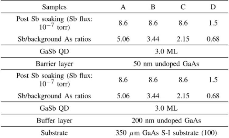
Four samples with bi-layer QDs structure investigated in this letter are grown on (100)-oriented semi-insulated GaAs substrate by used the Riber compact-21 solid-source MBE system. In this system, effusion cells with crackers and needle valves are adopted for both the As and Sb sources. To investigate the influence of Sb/background As ratio during the post-growth soaking procedure on the GaSb ring formation, samples with different ratio values are prepared. The sample structures are shown in Table I. The pre- and post- Sb soaking times adopted for the samples are 15 and 120 sec., respectively. For samples A, B and C, to prevent QR formation, the Sb needle valve is fully opened to reach a higher Sb beam equivalent flux pressure (BEP) 8.6 × 10⁻⁷ torr during the post Sb soaking procedure. Although the As shutter is closed during the post soaking procedure, by changing the needle valve of the As shutter, the Sb/background As BEP flux ratios would still change from 5.06, 3.44 to 2.14 for samples
1204 IEEE PHOTONICS TECHNOLOGY LETTERS, VOL. 24, NO. 14, JULY 15, 2012
TABLE I
WAFERSTRUCTURES OF THESAMPLESA, B, C,ANDD
Samples A B C D
Post Sb soaking (Sb flux:
10−7torr) 8.6 8.6 8.6 1.5 Sb/background As ratios 5.06 3.44 2.15 0.68
GaSb QD 3.0 ML
Barrier layer 50 nm undoped GaAs Post Sb soaking (Sb flux:
10−7torr) 8.6 8.6 8.6 1.5 Sb/background As ratios 5.06 3.44 2.15 0.68
GaSb QD 3.0 ML
Buffer layer 200 nm undoped GaAs Substrate 350µm GaAs S-I substrate (100)
A, B and C, respectively. With similar growth procedure, samples D is prepared with lower Sb BEP 1.5 × 10⁻⁷ torr during the post soaking procedure. The Sb/background As flux ratio for the sample is 0.68. For the EL observation of the QR structure, an additional sample with a single GaSb QR structures with the same growth conditions of sample D is prepared on a (100) n-type GaAs substrate. The single QR layer is inserted in the center of a 400 nm undoped GaAs layer cladding by 300 nm p-type (p= 2 × 1018cm−3) and 200 nm n-type (n= 2 × 1018 cm−3) GaAs layers.
III. RESULTS ANDDISCUSSION
The 1 × 1 µm2 AFM images of the samples A, B and C with different Sb/background As ratios and the scanning-tunneling microcopy (STM) images of a single GaSb dot/ring are shown in Fig. 1. As shown in the AFM images, QDs without any QRs are observed for sample A. It is shown that under high Sb/background As flux ratios, GaSb QD mor-phologies can be well maintained. However, with decreasing Sb/background As ratios as the case for samples B and C, QRs would gradually appear on the AFM images. The dots/rings densities for samples A, B and C are 3.27/0, 1.93/0.69 and 1.03/1.72 × 1010 cm−2, which would correspond to 100, 74 and 37% in percentage, respectively. The results suggest that even under high Sb irradiation and As shutter closed conditions, the background As would still induce ring for-mation given Sb/background As flux ratios lower than ∼5.0. Also observed in the figure are the reduced QD/QR height 5.2/-, 2.5/1.1 and 2.2/1.3 with decreasing Sb/background As ratios for samples A, B and C, respectively. The phenomenon indicates that the formation mechanism of the QRs is attributed to the Sb atoms repelled from the QD summits results from the As-for-Sb exchange and the large strain on the summits [8]. The similar diameters of the dot and the ring shown in the STM images have also confirmed the formation mechanism of GaSb QRs.
The 10 K PL spectrums of samples A, B and C are shown in Fig. 2. As shown in the figure, the PL intensities would increase with decreasing Sb/background As flux ratios. The results suggest that with decreasing Sb/background As ratios, the severe As-for-Sb exchange may result in a less
250 nm Sample A Sample B Sample C 250 nm 250 nm 25 nm Dot Ring
Fig. 1. The 1× 1 µm2AFM images of the samples A, B, and C, and the STM images of a single GaSb dot/ring.
1.00 1.05 1.10 1.15 1.20 1.25 P L In te ns ity (a .u.) Energy (eV) 10 K Sample A Sample B Sample C
Fig. 2. The 10 K PL spectrums of samples A, B, and C.
abrupt GaSb/GaAs interfaces. In this case, more electron-hole wave function overlapping would be obtained for the type-II nano-structures such that the optical recombination probability would increase [9]. Also observed in the figure is the PL peak red shift instead of blue shift. Due to decreasing QD/QR heights are observed with decreasing Sb/background As flux ratios, the PL peak red shift is in contrary with the theoretical prediction of blue shift with reduced nano-structure sizes. Due to high Sb flux is adopted during the post soaking procedure for the three samples, it is possible that the excess Sb atoms would incorporate into the top capping GaAs layers. In this case, GaSb/GaAsSb instead of GaSb/GaAs interfaces are obtained between the GaSb QRs and GaAs layers. Therefore, with decreasing Sb/background As flux ratios, the Sb compositions in the barrier layers would decrease, which would result in the conduction band edge lowering in the GaAsSb barrier layers. The results would be a PL peak red shift with decreasing Sb/background As flux ratios.
To further investigate the influence of high background As pressure on the structure, sample D with lower Sb BEP 1.5 × 10⁻⁷ torr to achieve a even lower Sb/background As flux ratio 0.68 is prepared. The 1 × 1µm2 AFM image of sample D is shown in Fig. 3(a). As shown in the figure, all the GaSb QDs have been transformed into QRs. The results have demonstrated that given much lower Sb/background As flux ratios, the background As is already sufficient to convert all the GaSb QDs into QRs even if the As shutter is closed. The 10 K PL spectrums of samples A, C and D are shown
LIN et al.: ROOM-TEMPERATURE ELECTRO-LUMINESCENCE OF TYPE-II GaSb/GaAs QUANTUM RINGS 1205 250 nm Sample D (a) 0.96 1.02 1.08 1.14 1.20 1.26 1.32 10 K Sample A Sample C Sample D PL Intensity (a. u.) Energy ( eV ) (b)
Fig. 3. (a) The 1 × 1 µm2 AFM image of sample D and (b) 10 K PL spectrums of samples A, C, and D.
in Fig. 3(b). As shown in the figure, increasing PL intensities with decreasing Sb/background As flux ratios are observed. Compared with sample A, the PL intensity of sample D is
∼20 times higher. Since severe As-for-Sb exchange and QR
formation are observed with decreasing Sb/background As flux ratios, there are two possible mechanisms responsible for the PL intensity enhancement of GaSb QRs. One is the less abrupt GaSb/GaAs interfaces resulted from the severe As-for-Sb exchange as observed for samples D with low Sb/background As flux ratios such that electron-hole wave function overlapping would increase. The other is the more surrounding electron shells over the GaSb QRs such that compared with QDs, higher optical recombination rate would be observed for GaSb QRs [10].
Since enhanced PL intensity is observed for the QR struc-ture as the case of sample D, a GaSb QR PIN diode with the same growth conditions of sample D is prepared to demon-strate its possible application in light-emitting devices. The room-temperature EL spectrum under 0.7 mA and 100 MHz pulsed injection current of the device is shown in Fig. 4. As shown in the figure, a significant EL spectrum with peak at ∼1.05 eV is observed for the device, which is close to the value observed from the PL spectrum of sample D. The results suggest that high optical recombination probability can be observed for this structure. The EL peaks observed at different injection currents are shown in the insert figure of Fig. 4. A linear dependence of the EL peak with the third root of the injection currents is observed, which has confirmed the origin of the luminescence to be from the type-II GaSb/GaAs QR structures [11]. 0.4 0.6 0.8 1.0 1.2 1.4 1.6 1.02 1.03 1.04 1.05 1.06 1.07 1.08 EL Peak Energy ( eV ) Current1/3 (mA1/3 ) 0.9 1.0 1.1 1.2 1.3 1.4 1.5 300 K 0.7 mA E L In te ns it y (a .u .) Photon Energy ( eV )
Fig. 4. Room-temperature EL spectrum of the GaAs PIN diode with a single GaSb QR layer under a 0.7-mA injection current. Inset: linear dependence of EL peaks with the third root of the injection currents.
IV. CONCLUSION
In conclusion, the influence of Sb/background As flux ratios on GaSb nano-structures is investigated in this letter. Ring for-mation and enhanced PL intensities are observed with decreas-ing Sb/background As flux ratios. Room-temperature EL of a single GaSb QR layer embedded in a GaAs PIN diode is also demonstrated. The results have indicated different research directions for GaSb nano-structures in device applications. Since enhanced luminescence is observed for GaSb QRs, the structures are more advantageous in the application of optical devices like LEDs and laser diodes. As for the applications of GaSb QDs in electronic devices, high Sb/background As flux ratios should be adopted to prevent QR formations.
REFERENCES
[1] F. Hatami, et al., “Radiative recombination in type-II GaSb/GaAs quantum dots,” Appl. Phys. Lett., vol. 67, no. 5, pp. 656–658, 1995.
[2] S. Y. Lin, et al., “Room-temperature operation type-II GaSb/GaAs quantum-dot infrared light-emitting diode,” Appl. Phys. Lett., vol. 96, no. 12, pp. 123503–123505, 2010.
[3] C. C. Tseng, W. H. Lin, S. Y. Wu, S. H. Chen, and S. Y. Lin, “The transition mechanisms of type-II GaSb/GaAs quantum-dot infrared light-emitting diodes,” J. Cryst. Growth, vol. 323, no. 1, pp. 466–469, 2011. [4] W. H. Lin, et al., “Wavelength-tunable InGaAs-capped quantum-dot infrared photodetectors for multi-color detection,” Infr. Phys. Technol., vol. 54, no. 3, pp. 220–222, 2011.
[5] M. Geller, C. Kapteyn, L. Müller-Kirsch, R. Heitz, and D. Bimberg, “450 meV hole localization in GaSb/GaAs quantum dots,” Appl. Phys.
Lett., vol. 82, no. 16, pp. 2706–2708, 2003.
[6] R. Timm, et al., “Self-organized formation of GaSb/GaAs quantum rings,” Phys. Rev. Lett., vol. 101, no. 25, pp. 256101–256104, 2008. [7] K. Suzuki, R. A. Hogg, K. Tachibana, and Y. Arakawa, “Density
control of GaSb/GaAs self-assembled quantum dots (∼25 nm) grown by molecular beam epitaxy,” Jpn. J. Appl. Phys., vol. 37, no. 2B, pp. L203–205, 1998.
[8] C. C. Tseng, et al., “Influence of as on the morphologies and optical characteristics of GaSb/GaAs quantum dots,” IEEE J. Quantum
Elec-tron., vol. 47, no. 3, pp. 335–339, Mar. 2011.
[9] T. Kawazu and H. Sakaki, “Effects of Sb/As intermixing on optical properties of GaSb type-II quantum dots in GaAs grown by droplet epitaxy,” Appl. Phys. Lett., vol. 97, no. 26, pp. 261906–261908, 2010. [10] S. Kobayashi, C. Jiang, T. Kawazu, and H. Sakaki, “Self-assembled
growth of GaSb type II quantum ring structures,” Jpn. J. Appl. Phys., vol. 43, no. 5B, pp. L662–L664, 2004.
[11] D. Alonso-Álvarez, B. Alén, J. M. García, and J. M. Ripalda, “Optical investigation of type II GaSb/GaAs self-assembled quantum dots,” Appl.