國 立 交 通 大 學
顯示科技研究所
碩 士 論 文
低溫鈍化技術於多功能薄膜之研究與應用
Application of low temperature passivation for
muti-funtional thin film
研 究 生 : 鄭 逸 立
指導教授 : 劉 柏 村 博士
低溫鈍化技術於多功能薄膜之研究與應用
Application of low temperature passivation for
muti-funtional thin film
研 究 生:鄭 逸 立 Student:Yi-Li Cheng
指導教授:劉 柏 村 博士 Advisor:Dr. Po-Tsun Liu
國 立 交 通 大 學
顯 示 科 技 研 究 所
碩 士 論 文
A Thesis
Submitted to Department of Photonics and Display Institute College of Electrical and Computer Engineering
National Chiao Tung University in Partial Fulfillment of the Requirements
for the Degree of Master
in Photonics June 2008
Hsinchu, Taiwan, Republic of China
低溫鈍化技術於多功能薄膜之研究與應用
研究生:鄭 逸 立 指導教授:劉 柏 村 博士
國 立 交 通 大 學
光電工程學系 顯示科技研究所
摘要
在此論文裡,我們研究了介電常數材料在超臨界二氧化碳流體混合水的熱處 理下其電性的改變。首先,在室溫下,利用電子束蒸渡系統成長極薄的氧化矽薄 膜,厚度約為 7 奈米,為了取代傳統的高溫退火製程,能在未來於玻璃基本上運 用。使用了溫度約 150°C 超臨界流體混合水的技術,為了驗證超臨界流體混合水 能有效的使水分子進入到氧化矽,進而減少薄膜的缺陷密度,我們經由紅外線光 譜儀、熱脫附常壓游離質譜儀與 X 射線光電子能譜來做材料分析,結果均顯示於 氧化矽薄膜內氧的含量增加,而厚度為 7 奈米氧化矽薄膜在閘極電壓 3 伏特的操 作下,其單位面積漏電流約為 2×10⁻⁷ A/cm2,並且得到較高的崩潰電壓,崩潰電壓 約為 6 伏特,傳導機制亦由原本未經過處理的量子穿隧效應轉換為熱放射效應, 以上主要的原因是由於氧化矽薄膜的缺陷密度減少。 除此之外,我們發現在超臨界二氧化碳流體混合水處理過後的薄膜擁有非揮 發性電阻式記憶體的特性。並且量測了其儲存的時間,可靠度,提出了相關的物 理模型去解釋其儲存的成因。藉由薄膜內部處理過後剩餘的缺陷,施加足夠的偏 壓下,使其缺陷內部電子發生局部穿隧的情形,進而改變能帶。產生了電阻的改 變,達到記憶體的特性。 由這些結果均顯示,藉由超臨界流體混合水的技術,能減少薄膜的缺陷密度。 並且也能在低溫下製造出記憶體。可預期的,若超臨界流體的特殊特性整合在介 電常數材料、薄膜電晶體、太陽能電池與記憶體製程上,將具有其優勢。Application of low temperature
passivation for muti-funtional thin film
Student:Yi-Li Cheng Advisor:Dr. Po-Tsun Liu
Department of Photonics and Display Institute
National Chiao Tung University
Abstract
In this study, supercritical fluids (SCF) technology is employed originally to effectively improve the properties of low-temperature-deposited silicon oxide dielectric films. In this work, 7 nm ultra-thin Silicon Oxide (SiOx) films are fabricated by e-gun
method at room temperature, and replacing the conventional high temperature annealing with supercritical fluids treatment at 150 °C. The supercritical fluids act a transporter to deliver H2O molecule into the SiOx films for repairing defect states. After this proposed
process, the absorption peaks of Si-O bonding apparently raise and the quantity of oxygen in SiOx film increases from FTIR and TDS measurement, individually. The
leakage current density of 7 nm SiOx film is cut down to 2×10 -7
A/cm2 at |Vg| = 3 V, and the conduction mechanism is transferred from quantum tunneling to thermal emission because of the significantly reducing the defects in the SiOx film. Moreover, the higher
breakdown voltage is obtained, reaching |Vg| = 6 V.
Additionally, the RRAM characteristics was found in SiOx film treated by
supercritical fluid,and retention,endurance were measured.when less trap was in treated film,the bias was applied enough on film,that made tunning effect happened inside.The resistence changed was by binding energy .
誌 謝
這兩年以來受到許多人幫助及教導。首先要感謝我的論文指導教授劉柏村博 士,帶我知道研究的領域及待人接物的處理。以及感謝中山物研教授張鼎張博士 對實驗的方向及內容有許多的協助,誠摯的感謝老師的幫助。以及諸位口試委員 得指導讓實驗的內容更為完善。 並且感謝蔡志宗學長在超臨界流體技術中帶領我一窺奧秘,以及論文中多所 協助及指導。此外楊柏宇學長、周誼明學長、高逸侑學長對實驗機台及內容的教 導也是由衷的感謝。還有要感謝陳緯仁學長、吳興華學長、鄒一德學長、陳世青 學長、葉炳宏學長、曹書瑋學長、馮立偉學長、弘偉學長,盧皓彥學長感謝學長 們平日對我的照顧以及研究上的建議。也要感謝實驗室一起工作的同學-郭豫 杰、竹立煒、林威廷、陳巍方、王超駿、張繼聖、蔡尚祐、陳思維…等,以及學 弟-王信淵、張耿維…等,因為有了你們在這兩年的過程中多了許多歡樂。還有 NDL 及奈米中心許多的工程人員在這兩年的過程中感謝諸位的協助,尤其奈米中心 的林先生感謝你在製程上許多建議及協助。 最後感謝我的父母親,鄭金漳先生以及呂秋菊女士。如果沒有您們在我的背 後提供需多協助及幫忙,將不能心無旁誤的把心力用在實驗上面。 鄭逸立 2008 年 6 月Contents
Chapter 1 Introduction
1.1 Supercritical Fluid Technology --- 1
1.2 General Background --- 2
1.2.1 Low temperature Oxide dielectric film --- 2
1.2.2 Nonvolatile resistive switching memory --- 3
1.3 Motivatio --- 4
Chapter 2 Application of Supercritical Fluid Technology on Silicon-Oxide
Dielectric Thin Film
2.1 Fabrication of Metal-Insulator-Silicon (MIS) and Experiment Process - 5 2.2 Analysis of Material and Discussion --- 62.2.1 Fourier Trans-form Infrared Spectroscopy (FTIR) Analysis --- 6
2.2.2 Thermal Desorption System – Atmospheric Pressure Ionization Mass Spectrometer (TDS-APIMS) Analysis --- 7
2.2.3 X-ray Photoelectron Spectroscopy (XPS) Analysis --- 7
2.2.4 Auger Electron Spectroscopy (AES) Analysis --- 9
2.3 Analysis of Electrical Characteristics and Discussion --- 10
2.3.1 The current density-electric field (J-E) characteristics --- 10
2.3.2 Conduction Mechanism --- 10
2.3.3 The capacitance-voltage (C-V) characteristics --- 14
2.3.4 Breakdown voltage measurement and gate bias stress --- 15
2.4 Summary --- 17
Chapter 3 Application of Supercritical Fluid Technology on
Resisitive
Random Access Memory
3.1 Fabrication of Non-volatile Memories and Experiment Process --- 183.2.1 The current density-electric field (J-E) characteristics --- 20
3.2.2 Retention --- 22
3.2.3 Endurance --- 22
3.2.4 Basic Program/Erase Mechanisms --- 23
3.3 Summary --- 24
Chapter 4 Conclusion --- 26
References
Table Captions
Chapter 1
Table 1-1 Critical temperature and pressure for some common fluids. --- 28Table 1-2 Comparison of physical properties of CO2. --- 28
Chapter 2
Table 2-1 Summary of binding energies for ultra thin SiOx films. --- 41Table 2-2 Summary of binding energies for ultra thin SiOx films O 1s after various post-treatments, including SCCO2-only, H2O vapor and 3000psi-SCCO2 treatment. --- 42
Table 2-3 The extracted parameters from C-V curves of SiOx films after different treatment. --- 42
Figure Captions
Chapter 1
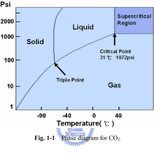
Fig. 1-1 Phase diagram for CO2. --- 27
Fig.1-2 Density-pressure-temperature surface for pure CO2. --- 27
Chaprer 2
Fig. 2-1 The supercritical fluid system. --- 29 Fig. 2-2 The experiment processes of thin SiOx film with various treatments. --- 30
Fig. 2-3 The FTIR spectra of SiOx films after various post-treatments, including
SCCO2-only, H2O vapor and 3000psi-SCCO2 treatment, and the un-treated
SiOx film is taken as background. --- 31
Fig. 2-4 The transporting mechanism for SCCO2 fluids taking H2O molecule into SiOx
film.. --- 32 Fig. 2-5 The thermal desorption spectroscopy (TDS) measurement, (a) m/e
(mass-to-charge ratio) = 18 peak that is attributed to H2O, (b) m/e = 32 peak
that is attributed to O2. --- 33
Fig. 2-6 The X-ray photoemission spectra of SiOx films Si 2p after various
post-treatments, including (a) SCCO2-only, (b) H2O vapor and (c)
3000psi-SCCO2 treatment. --- 34
Fig. 2-7 The X-ray photoemission spectra of SiOx films O 1s after various
post-treatments, including (a) SCCO2-only, (b) H2O vapor and (c)
3000psi-SCCO2 treatment. --- 35
Fig. 2-8 Auger electron spectroscopy: (a) SCCO2-only treatment (b) H2O vapor
Fig. 2-9 Conduction mechanism for Al/SiOx/Si MIS structure. --- 37
Fig. 2-10 The leakage current densities of SiOx films after different
treatments.(Thenegative bias is applied on gate electrode) --- 37 Fig. 2-11 (a) Curve of ln (J/E) versus reciprocal of electric field (1/E) for the
SCCO2-only treated SiOx film, and a schematic energy band diagram
accounting for trap-assisted tunneling shown in the inset. (b) Leakage current density versus the square root of electric field (E1/2) plot for the 3000 psi-SCCO2 treated SiOx film. The inset shows the energy band diagram
of Schottky-type conduction mechanism. --- 38 Fig. 2-12 The leakage current densities of SiOx films after different treatments (The
positive bias is applied on gate electrode). Inset plots the energy band diagram of leakage current.--- 39 Fig. 2-13 The capacitance-voltage characteristics of SiOx films after different t
reatment, measuring at 1M Hz with gate bias swing. --- 39 Fig. 2-14 The breakdown characteristic curves of SiOx films after various treatments
at negative gate bias region.. --- 40 Fig. 2-15 The variation of leakage current of different-treated SiOx films as a function
of stress time at a high electric field = 3.8 MV/cm. --- 41
Chapter 3
Fig. 3-1 shows the current density (J) of SiOx film treated by 3000 psi SCCO2 fluid
as a function of bias voltage. --- 43 Fig. 3-2 A linear dependence indicates the trap-assisted tunneling dominates current
t ransport mechanism while applying larger negative bias than –0.8 V -- 43 Fig. 3-3 The current characteristic curves of SiOx film treated by H2O vapor --- 44
Fig. 3-4 the P-F emission dominates the conduction mechanism while applying larger
negative bias than –1 V --- 44
Fig. 3-5 displays the current characteristic curves of SiOx film treated by 3000 psi SCCO2 fluid mixed with ethyl alcohol and H2O. --- 45
Fig. 3-6 The plot of ln (J/E) versus square root of applied electric field (E1/2) ---- 45
Fig. 3-7 The retention properties reated at H2O vapor --- 46
Fig. 3-8 The retention properties treated at SCCO2-col--- 46
Fig. 3-9 Endurance for SCCO2 co-solvent treatment embedded in SiOx film--- 47
Fig. 3-10 the SET and RESET voltage for samples --- 47
Fig. 3-11 show the retention characteristics of two resistance states at room temperature for the SiOx films--- 48
Fig. 3-12 movement of carrier between trap states in SiOx gap, and a possible mechanism. --- 48
Chapter 1
Introduction
1.1 Supercritical Fluid Technology
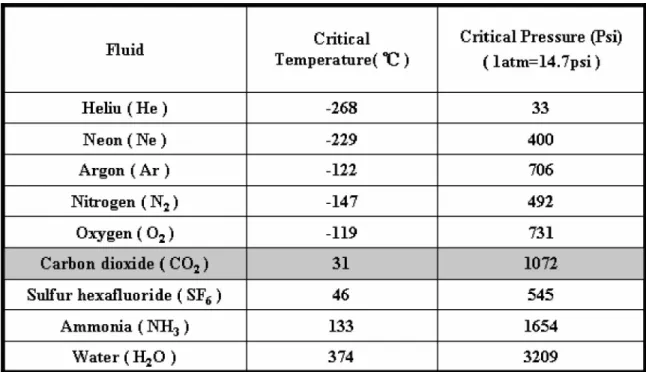
Supercritical fluids are compounds above their critical temperatures and pressure, as shown in Fig 1-1 [1, 2]. The attractiveness of supercritical fluids for commercial applications is their unique combination of liquid-like and gas-like properties. The Table 1-1 shows critical temperature and pressure for some common fluids. CO2-based
supercritical fluids are particularly attractive because CO2 is non-toxic, non-flammable,
and inexpensive. Besides, its critical conditions are easily achievable with existing process equipment (31 °C, 1072 psi =72.8 atm).
Figure 1-2 shows the density-pressure-temperature surface for pure CO2. It can
be discovered that relatively small changes in temperature or pressure near the critical point, resulting in large changes in density. Table 1-2 shows the comparison of several physical properties of typical liquid, vapor, and supercritical fluid state for CO2. It
could be seen that supercritical CO2 (SCCO2) fluids possesses liquid-like density, so
that SCCO2 fluids are analogous with light hydrocarbon to dissolve most solutes and
own exceptional transport capability [3, 4]. On the other hand, SCCO2 fluids hold
gas-like characteristic due to their viscosity and surface tension are extremely low, it allows SCCO2 fluids to keep fine diffusion capability and enter the nano-scale pores or
spaces without damage. These properties are the reasons for SCCO2 fluids to employ
in many commercial applications, including the extraction of caffeine from coffee, fats from foods, and essential oils from plants for using in perfumes. Furthermore, in last years, many records are investigated with SCCO2 fluids to apply in semiconductor
fabrication, such as cleaning wafer and stripping photoresist, by means of its high mass transfer rates and infiltration capabilities [4-6].
1.2 General Background
1.2.1 Low temperature Oxide dielectric films
In the recent years, Low-temperature polycrystalline silicon (LTPS) thin-film transistors have been widely studied because of their potential applications in high-performance displays Together with improvements in display technology, the low-temperature polysilicon (LTPS) TFT LCD is expected to be one of the most promising displays for digital tools such as Liquid crystal display and PDA.
SiOx thin film is known to have excellent properties such as hardness, wear-resistance, anti-corrosion and also optical, dielectric properties, so it is widely applied as the gate dielectric of transistor and the tunneling oxide of non-volatile memory. [7-9] The total does radiation hardess of the gate insulator used in MOS devices is strogly determined by the details of the oxide growth and annealing process. The development of low cost, rugged plastic and glass displays could lead to a dramatic increase in both the variety and utility of military and consumer display products. the added feature of flexibility may lead to the creationof entirely new display markets. The primary advantages of plastic and glass substrates with respect to silicon are a reduction in theweight of the display, flexibility, and a reduction in display breakage, both during fabrication and use Additionally. A growing demand for new applications of thin film microelectronicsin portable lightweight systems has resulted in a need for reduced maximum processing temperatures during fabrication of integrated circuits. For example, in the flat panel display industry researchers are continually lowering processing temperatures required to form the polycrystalline
1.2.2 Nonvolatile resistive switching memory
Since the first observation of bistable resistance states in the 1960’s, reversible and reproducible resistance switching phenomena caused by applied electric field have been investigated widely to be used as resistive random access memories (RRAM). Recently, numerous metal oxides and perovskite oxides including Nb2O5, TiO2, and Nb-doped SrTiO3 have been reported for RRAM applications. Nevertheless, there is only few studies mention the process of resistance memory at low temperature. The binary oxide MIM memory devices were discovered decades ago [10]. This device had not been a serious contender for large scale memory array application. After the publication of electric-pulse-induced reversible (EPIR) resistance non-volatile memory by Liu et al in 2000 the ternary MIM memory, which we referred as RRAM, devices have attracted considerable interest. Resisitive RAM (RRAM) development is generally based on using an electrical pulse to change the resistance across a thin film of either a simple binary metal oxide or a more complex perovskite oxide. It has been the focus for reearch at several device manufacturers and some startups because it promises high density, low cost and low power consumption, along with non-volatility. It has the classic profile of the much-sought-after universal memory that could combine the speed of SRAM with density of DRAM and the nonvolatility of flash memory.
1.3 Motivation
In recent years, many reports interests in the formation of SiOx film at low
temperature (≦ 200 °C) for fabricating electron devices on flexible plastic substrates. [11-13] Among various deposition methods, the physical vapor deposition (PVD) is favorable as a result of the advantages of simple process, low cost, and conformity with low-temperature fabrication. Nevertheless, a high temperature annealing or plasma treatment is generally taken as post-treatment to passivate the traps in PVD-deposited film for improving the dielectric characteristics. Due to the limit of glass transition temperatures (Tg), these high temperature post-treatments are
unsuitable to plastic substrates,6 and a low temperature treatment to passivate traps is required.
the SCCO2 fluid is proposed to fabricate the resistance memory at 150 °C, so it
would be applicable to product RRAM on the substrates with low glass transition temperatures (Tg). The supercritical fluid technology is generally used for the impurity
extraction, dehydration and drying of materials with a fine structure. It also had employed SCCO2 fluid to deliver oxidant into metal oxide film for terminating electric
defects by the gas-like and liquid-like properties. According to the mechanisms of bistable resistance states are possibly dominated by some kind of charge trap, the we would employ SCCO2 technology to fabricate a resistance memory by varying the trap
density in SiOx film. The experimental works will focus on the effect of passivating
traps by SCCO2 treatment and investigate the influence of varying trap density on
Chapter 2
Application of Supercritical Fluid Technology
on Silicon-Oxide Dielectric Thin Film
2.1 Fabrication of
Silicon-Oxide
and Experiment Process
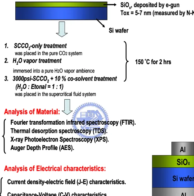
The e-gun system was used to deposit SiOx films on p-type (100) silicon wafer
under 2 ×10⁻⁶ torr at room temperature, and the average thickness of SiOx films
measured by ellipsometer system is 5-7 nm. For enhancing the quality of these ultra-thin SiOx films, three different post-treatments were applied individually. First
method, labeled as “H2O vapor treatment”, is immersing the SiOx film into a pure H2O
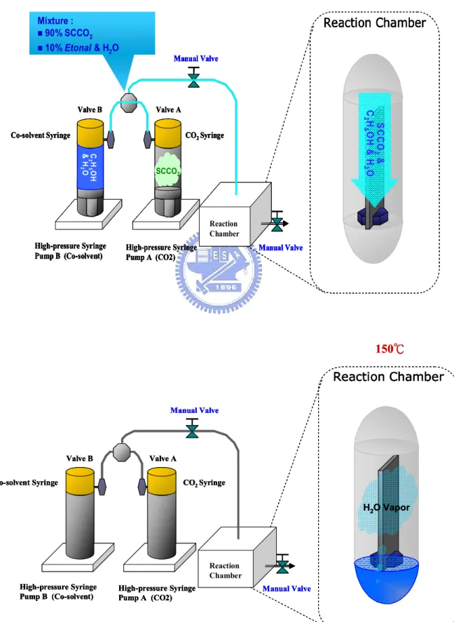
vapor ambience at 150 °C for 2 hrs, in a stainless steel chamber. Second method, labeled as “3000 psi-SCCO2 treatment”, is placing the SiOx film in supercritical fluid
system at 150 °C for 2 hrs, where was full of 3000 psi-SCCO2 fluids mixed with 8
vol.% ethyl alcohol and 2 vol.% pure H2O. The ethyl alcohol acts surfactant between
nonpolar SCCO2 fluids and polar H2O molecules to making the uniform distribution of
H2O molecules in SCCO2 fluids, and the SCCO2 fluids thereby could transport H2O
molecules efficiently into SiOx layer to react with traps. In comparison with 3000
psi-SCCO2 treatment, the third method is treating SiOx film with 3000 psi pure SCCO2
fluids but no co-solvent was added, and labeled as “SCCO2-only”. The supercritical
fluid system is shown in Fig. 2-1.Afterward, the Al metal was thermally evaporated on the top surface of these treated SiOx films and the backside of silicon wafer as
electrodes to shape the metal insulator semiconductor (MIS) structure. The Fourier transformation infrared spectroscopy (FTIR) was applied to determine the evolution of chemical functional bonding after different treatment. The atomic content of SiOx film
was detected from Auger electron spectroscopy (AES) analysis, and the electrical behaviors of SiOx film were measured by HP 4156-A semiconductor analyzer and
Agilent 4284A CV meter. The experiment processes of thin SiOx film with various
treatments are exhibited in Fig. 2-2.
2.2 Analysis of Material and Discussion
2.2.1 Fourier Trans-form Infrared Spectroscopy (FTIR) Analysis
The FTIR spectra of SiOx films after different treatments are shown in Fig. 2-3,
and the un-treated SiOx film is taken as background. For SCCO2-only treated SiOx film,
there is no IR absorption peak appears in the wavenumber of 400-1500 cm−1, i.e. the SCCO2 fluid wouldn’t affect the functional structure of SiOx. In the case of H2O-vapor
treated SiOx film, however, vibration bands for Si–O stretching at 1080 cm−1, Si=O
stretching at 1230 cm−1, Si–O rocking at 440 cm−1, and S-H bending at 610 cm-1 increase clearly. [14]The raise of IR absorption peak indicates that the H2O molecules
could infiltrate into SiOx film and modify the quality of SiOx film during H2O-vapor
process. Because the main variation occurs in S-O bonding, it is believed that the H2O
molecule is operative oxidant to react with Si dangling bond, and this agrees with prior literatures. [15~16] The same IR absorption peaks are also observed for 3000-psi SCCO2 treated SiOx film, and the higher absorption peaks express that SCCO2 fluid
added with co-solvent (8 vol.% ethyl alcohol and 2 vol.% H2O) is a more operative
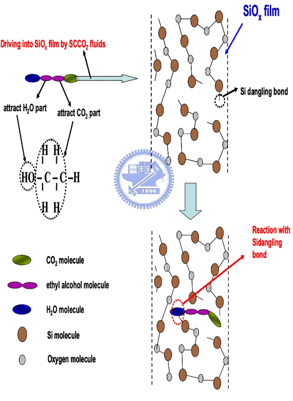
method than H2O-vapor to enhance the quality of SiOx films. Therefore, the SCCO2
fluids mixed with co-solvent would completely infiltrate in into SiOx films as the pressure increasing in 3000psi, and the best improvement for SiOx films is achieved because of advancing the reaction probability between H2O molecule and Si dangling
bonds. , and the transporting mechanism for SCCO2 fluids taking H2O molecule into
2.2.2 Thermal Desorption System – Atmospheric Pressure Ionization Mass Spectrometer (TDS-APIMS) Analysis
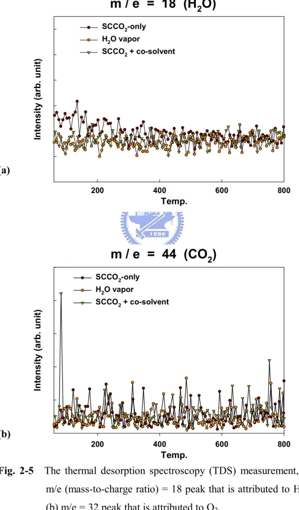
The TDS measurement, as shown in the Fig. 2-5, was carried out upon heating these treated SiOx films from 50 to 800 °C at a heating rate of 10 °C/min in vacuum
(10−5 Pa.). In Fig. 2-5 (a), m/e (mass-to-charge ratio) = 18 peak that is attributed to H2Owas monitored to evaluate the content of residual moisture in SiOx films. It is
clearly found the same H2O content is detected in the SCCO2-col, H2O-vapor and
3000 psi-SCCO2-treated SiOx film, certainly consistent with the FTIR observation.
From Fig. 2-5 (b), m/e (mass-to- charge ratio) = 44 peak that is attributed to CO2, the
residual CO2 in SiOx is equal the same after 3000 psi-SCCO2 , H2O-vapor and pure
SCCO2 treatment. This is result from SCCO2-col, , H2O-vapor and pure SCCO2
treatment mean that no residual moisture and CO2 in the SiOx film. Therefore
different Electrical Characteristics were not induced by residual moisture and CO2.
2.2.3 X-ray Photoelectron Spectroscopy (XPS) Analysis
XPS involves measuring the photoelectron spectra obtained when a sample surface is irradiated with x-rays. The kinetic energy (peak position) of the photoelectrons can be written as
-E - -q h
EK B s
where h is the x-ray energy, EB is the binding energy (the difference between
the Fermi level and the energy level being measured), is the work function of the s electron spectrometer, q is the electronic charge, and is the surface potential.
We have also performed XPS measurements using an Al Kα X-ray source (1486.6 eV photons) to determine the bonding environments of the Si and O atoms. the XPS spectra for Si 2p level that were calibrated from C 1s peak at 284.5 eV. Each spectrum was represented the result at different post-treatments, including SCCO2-only,
H2O vapor and 3000psi-SCCO2 treatment. The first group labeled as pure SCCO2
treatment, was designed as the control sample, and was only is treating SiOx film with
3000 psi pure SCCO2 fluids but no co-solvent was added,s. The second group labeled
as H2O vapor treatment, was immersed into a pure H2O vapor ambience at 150 °C for
2 hrs in a pressure-proof stainless steel chamber with a volume of 30cm3. The third group marked as 3000psi-SCCO2 treatment, was placed in the supercritical fluid
system at 150°C for 2 hrs, where was injected with 3000psi of SCCO2 fluids mixed
with 5 vol.% of ethyl alcohol and 5 vol.% of pure H2O. As shown in Figure 2-6 , the
Si2p peak, which have binding energies of 103.9 and 99 eV, respectively related to Si-O bonding and Si=Si in SiOx. However, the binding energy of Si2p peak shown in
Figure 2-6 varied from 103.8 eV for pure SCCO2 fluids sample to 104.1 eV for
3000psi-SCCO2 treatment sample. The origins of binding energy shift (ΔBE) are
suggested as a number of factors such as charge transfer effect, presence of electric field, environmental charge density, and hybridization. Among these, charge transfer is regarded as a dominant mechanism causing a binding energy shift. According to the charge transfer mechanism, removing an electron from the valence orbital generates the increment in core electron’s potential and finally leads a chemical binding energy shift [17]. Therefore, it is considered that the Si2Ppeaks shift originated from the
enhanced charge transfer with different post-treatments, i.e., the larger portion of Si atoms was fully oxidized with 3000psi-SCCO2 treatment. Figure 2-7 shows the O 1s
core level peaks also demonstrated binding energy shift with changing of different post-treatments. Each peak can be split into two sub-peaks by Gaussian fitting which represent the O-Si bonding at ~533 eV [18,19]. The peak intensity of O-Si bond for different treatments is not the same, meaning that these post-treatments would make different influence on the thickness and quality of the interfacial SiOx film. For the
H20 vapor SiOx film, however, the peak intensity of Si-O bands raises apparently in
comparison with the pure SCCO2 fluids -treated SiOx film. This is believed well that
the H2O vapor would permeate into SiOx film and makes reaction with Si dangling
deposited SiOx film could be thereby passivated by H2O vapor molecules. Furthermore,
with SCCO2 treatment, obvious increase in the intensity of Si-O bonding is observed in
the XPS. It indicates that the best transport efficiency of H2O molecules into SiOx film
is achieved by the SCCO2 fluids, potentially modifying the dielectric properties of SiOx
film, and the transporting mechanism for SCCO2 fluids taking H2O molecule into SiOx
film is shown in Fig. 2-4. Summary of binding energies for SiOx films are shown in
Table 2-1 and Table 2-2.
2.2.4 Auger Electron Spectroscopy (AES) Analysis
In order to analyze the composition of the silicon oxide film after various post-treatments, including pure SCCO2 fluids, H2O vapor and 3000 psi-SCCO2
treatment, we performed the Auger electron spectroscopy analysis. The first group labeled as pure SCCO2 fluids treatment, was designed as the control sample, and was
only treated in pure SCCO2 fluid at 150 °C for 2 hrs. The second group labeled as H2O
vapor treatment, was immersed into a pure H2O vapor ambience at 150 °C for 2 hrs in
a pressure-proof stainless steel chamber with a volume of 30cm3. The third group marked as 3000psi-SCCO2 treatment, was placed in the supercritical fluid system at
150°C for 2 hrs, where was injected with 3000psi of SCCO2 fluids mixed with 5 vol.%
of propyl alcohol and 5 vol.% of pure H2O. The ethyl alcohol plays a role of surfactant
between nopolar-SCCO2 fluids and polar-H2O molecules, so that the H2O molecule
uniformly distributes in SCCO2 fluids and be delivered into the SiOx film for
passivating defects. As shown in Figure 2-8, the pure SCCO2 fluids-treated and H2O
vapor-treated films has oxygen composition lower than that of the silicon oxide film after 3000 psi-SCCO2 treatment. The ethyl alcohol plays a role of surfactant between
nopolar-SCCO2 fluids and polar-H2O molecules, so that the H2O molecule uniformly
distributes in SCCO2 fluids and be delivered into the SiOx film for passivating defects.
2.3.1 The current density-electric field (J-E) characteristics
The plot of leakage current density of SiOx films versus electric field is displayed
in Fig2-10. to realize the influence of different treatment on dielectric characteristics. Among various post-treatments, the pure SCCO2 fluids SiOx film exhibits the most
serious leakage current, inferentially due to its poor dielectric characteristics with numerous traps inside the SiOx film. The improvement of electrical characteristics is
observed by using H2O vapor process, however, a high leakage current density still
appears at larger applied voltages. It could be inferred reasonably dependent on the defect passivation efficiency. The most indicating that H2O vapor can passivate the
traps (or defects) and alter dielectric properties of the low-temperature-deposited SiOx
film. After H2O vapor treatment, effective improvement of electrical characteristic is
obtained by the 3000 psi-SCCO2 treatment, exhibiting the lowest leakage current
density among all samples. Low leakage current density (less than 10-7 A/cm2). is kept constantly, even biased at an electric field of 3 MV/cm. The electrical performance agrees with FTIR analysis, in which 3000 psi-SCCO2 treatment modified SiOx
dielectrics even effectively.
2.3.2 Conduction Mechanism
There may be different conduction mechanisms in the insulator thin film, including Schottky-Richardson emission [23], Frenkel-Poole emission [23,24], Fowler-Nordheim tunneling [23,24], and trap assisted tunneling [25,26] illustrated in Fig 2-9. The Schottky-Richardson emission generated by the thermionic effect is caused by the electron transport across the potential energy barrier via field-assisted lowering at a metal-insulator interface. The leakage current governed by the Schottky-Richardson emission is as following:
A T exp E k T J 12 SR B SR 2 * SR
where
12 0 3SR q 4
, q is the electronic charge, A is the effective * Richardson constant, is the contact potential barrier,SR E is the applied electric field, is the permittivity in vacuum, 0 is the high frequency relative dielectric constant, Tis the absolute temperature, and k is the Boltzmann constant. We can B find the slope of the leakage current equation.
k T
T k E JSR SR 12 B ln A*T2 SR B ln T k SolpeSR BThe Frenkel-Poole emission is due to field-enhanced thermal excitation of trapped electrons in the insulator into the conduction band. The leakage current equation is:
J exp E k T J 12 FP B FP FP 0
where J0 0E is the low-field current density, is the low-field 0 conductivity,
120 3
FP q , q is the electronic charge, FP is the contact potential barrier,E is the applied electric field, is the permittivity in vacuum, 0 is the high frequency relative dielectric constant, Tis the absolute temperature, and
B
k is the Boltzmann constant. We can find the slope of the leakage current equation.
ln J k T
T k E J ln FP FP 12 B 0 FP B T k SolpeFP BThe Fowler-Nordheim tunneling is the flow of electrons through a triangular potential barrier. Tunneling is a quantum mechanical process similar to throwing a ball against a wall often results that the ball goes through the wall without damaging the wall or the ball. It also loses no energy during the tunnel event. The probability of this event happening, however, is extremely low, but an electron incident on a barrier typically several nm thick has a high probability of transmission. The Fowler-Nordheim tunneling current IFN is given by the expression [27]:
FN ox
ox FN G FN A A exp B I 2 where the A is the gate area, G is the oxide electric field, and ox AFN and BFN are usually considered to be constant. AFN and BFN are given as the following:
ox
B 6 B ox 3 FN q m m 8 h 1.54 10 m m A
3
12 B ox 7 2 1 3 B ox FN 8 2m 3eh 6.83 10 m m B where m is the effective electron mass in the oxide, m is the free electron mass, ox q
is the electronic charge, and is the barrier height at the silicon-oxide interface B given in units of eV in the expression for BFN. is actually an effective barrier B height that take into account barrier height lowering and quantization of electrons at the semiconductor surface. Rearranging IFN formula gives by:
FN
FN ox 2 ox FN 2 ox G FN A ln J ln A B I ln A plot of ln
JFN ox2
versus
1 ox
should be a straight line if the conduction through the oxide is pure Fowler-Nordheim conduction [27].In the trap assisted tunneling model, it is assumed that electrons first tunnel through the SiOX interfacial layer (direct-tunneling). Then, electrons tunnel through
traps located below the conduction band of the high-k thin film and leak to substrate finally [25]. The equation of leakage current density is [26]:
ox
oxexp E
E
J
From the equations as shown above, leakage current behaviors of insulate films can be investigated further on the leakage current density J electric field E
characteristics such as J vs. E12 plots.
The plot of the nature log of leakage current density versus the square root of the applied electric field was observed. It is found that the leakage current density is linearly related to square root of the applied electric field. The linear variations of the current correspond either to Schottky-Richardson emission or to Frenkel-Poole
conduction mechanism. For trap states with coulomb potentials, the expression is virtually identical to that of the Schottky-Richardson emission. The barrier height, however, is the depth of the trap potential well, and the quantity FP is larger than in the case of Schottky-Richardson emission by a factor of 2.
Leakage conduction mechanism is also investigated to support the comments on the electrical improvement of SiOx film. Fig. 2-11(a) plots ln (J/E) versus reciprocal of
electric field variation for the pure SCCO2 fluids treated SiOx film, and a schematic
energy band diagram accounting for leakage transport mechanism shown in the inset. A good linear fitting explains Fowler-Nordheim (F-N) tunneling [28] occurs in the electric fields higher than 1.2 MV/cm. Also, it is consistent with the electrical behavior of pure SCCO2 fluids treated SiOx film in Fig. 2-10 that leakage current density sharply
increases, while gate bias voltage larger than 1.2 MV/cm. This could be attributed to the trap-assisted tunneling due to numerous traps inside the 150°C- pure SCCO2 fluids
treated SiOx film [29]. For the 3000 psi-SCCO2 treated SiOx film, a plot of leakage
current density versus the square root of the applied field (E1/2) gives a good representation of the leakage behavior at high electric fields, as shown in Fig. 2-11(b). The leakage current density of the 3000 psi-SCCO2 treated SiOx is linearly related to
the square root of the applied electric field, demonstrating Schottky-Richardson emission transport mechanism [30]. The Schottky-type conduction can be verified by comparing the theoretical value of
120 3
SR q 4
with the calculated one obtained from the slope of the experimental curve ln J versus E1/2 [31], where q is the electronic charge, the dielectric constant of free space, 0 is the high frequency relative dielectric constant. The Schottky emission generated by the thermionic effect is caused by electron transport across the potential energy barrier via field-assisted lowering at a metal-insulator interface, shown in the insert of Fig. 2-11(b), and independent of traps. From the slope of ln J versus E1/2, the calculated value of relative dielectric constant ( ) is 3.5, and which is close to the determined value of 3.8 in capacitance-voltage (C-V) measurement (referring to table 2-3). This also proves, for 3000spi-SCCO2 treated SiOx film, the conduction mechanism is really Schottky
emission, but not trap-dependent Poole-Frenkel emission [31]. Additionally, the evolution of conduction mechanisms from trap-assisted tunneling to Schottky emission can confirm these defects inside low-temperature-deposited SiOx film is minimized
effectively by implementing the proposed SCCO2 technology. The leakage current
densities of SiOx films after different treatments are shown as a function of applied
positive gate bias voltage in Fig. 2-12, and the lower leakage current still could be acquired after 3000 psi-SCCO2 and H2O vapor treatment, especially treated with
SCCO2 fluids. This could be attributed to the influence of traps in the interface
between parasitical SiOx and Si wafer. Generally, in positive gate bias, the sources of
electron are (1) the interface states, (2) defects in depletion region, (3) back electrode of substrate, [33] and the later two source are negligible due to the p-type signal-crystal Si wafer is used in this work. For pure SCCO2 fluids treated SiOx film,
the great quantity of interface states still exist which generate electron-hole pair and lead to higher leakage current, as described in the inset of Fig. 2-12 After 3000 psi-SCCO2 treatment, the interface states were deactivated, hence the leakage current
is reduced. The reduction of interface states would be proved in capacitance-voltage measurement. [36]
2.3.3 The capacitance-voltage (C-V) characteristics
The capacitance-voltage (C-V) characteristics are also generally used to judge the quality of dielectric films. Figure 2-13 shows capacitance-voltage characteristics of SiOx films after different treatment, measuring at 1M Hz with gate bias swing from
negative voltage to positive voltage (forward) and from positive voltage to negative voltage (reverse). The slope of C-V curve in transient region, i.e. from Cmax to Cmin, is
relative to the interface states, for example, the sharp slope indicates fewer defects exist in the interface between SiOx and Si wafer. In Fig. 2-13, the pure SCCO2 fluids
-treated SiOx film presents the worst C-V curve and lower capacitance. This expresses
the lower dielectric constant, as shown in table 2-3, could be referred to the influence of defects in SiOx film. With H2O vapor treatment, the sharper C-V curve and higher
capacitance are obtained, and it could be attributed to the reduction of defects in SiOx
film and the interface. Furthermore, the best improvement is achieved by 3000 psi-SCCO2 treatment. This exhibits that the SCCO2 treatment possesses excellent
ability to passivate the defects, including Si dangling bonds and interface states.
Besides, from Fig. 2-13, the shift of C-V curve under forward and reverse swing is also appears in pure SCCO2 fluids and H2O vapor-treated SiOx films. It is resulted
from the trapped carrier in defects of SiOx films, and that is not expected for gate
insulator of transistors. Under negative gate bias, the electric inject from Al gate into SiOx films and trapped by defects, leading to the larger gate bias is required for
inducing electron-inversion layer. For describing clear, These results conform to the tendency in current-voltage characteristics and again verify that the SCCO2 technology
could effectively deactivate defects in SiOx films.The main reason could be referred to
the positively charged Si dangling bonds are passivated as a matter of fact, upon reducing the oxide thickness, it is difficult to calculate the density of interface states by using the high-low frequency method because of the substantially increased gate leakage current.
2.3.4 Breakdown voltage measurement and gate bias stress
Figure 2-14 show the breakdown characteristic curves of SiOx films after
various treatments at negative gate bias region, individually. The breakdown voltage is mainly relative to the qualities of dielectric films and the density of defects in the dielectric films. A large number of traps lead to the trap-assisted tunneling early occurs and a high leakage current appears at small electric field, such that the lower breakdown voltages of dielectric films comes up. In Fig. 2-15, whether at negative gate bias, the pure SCCO2 fluids -treated SiOx film presents the worst performance in
breakdown voltage are gradually achieved via H2O vapor and 3000 psi-SCCO2
treatment. This result exhibits clearly that the density of defects in SiOx films are
effectively reduced, and the breakdown voltage of 5~7nm SiOx film thereby could be
substantially ameliorated from 1 V to 10 V at negative gate bias. It also indicates that the SCCO2 fluids technology is greatly useful to enhance the low-temperature
deposited SiOx films by passivating defects, and allows the treated SiOx film holding
good reliability as the gate dielectric.
Another important property of dielectric films is the reliability under gate bias stress. Due to the gate dielectric is stressed at a high field when the transistors are operating, so that it is demanded for gate dielectric to have excellent resistance to the impairment under long time stress at operating electric field. During high electric field stress, the carriers of leakage current and high electric field would impact the weak bonding, leading to more defects, higher leakage current and the degradation of transistor [32]. Therefore, the reliability of dielectric under gate bias stress would judge whether agrees with the application of gate dielectric. Figure 2-15 shows the variation of leakage current of different-treated SiOx films as a function of stress time
at a high electric field = 3.8 MV/cm, where I0 is the initial leakage density. As well as
the tendency of the measurement of breakdown voltage, the pure SCCO2 fluids
-treated SiOx film behaves the most rises in the degree of leakage current as the stress time increasing, because of the great amount of defects and weak bonding. However, after treating with 3000 psi-SCCO2 process, the e-gun-deposited SiOx film performs a
fine reliability under high electric field stress, hence it is extremely suitable for the application of gate dielectric.
2.4 Summary
we have well improved the dielectric characteristics of e-gun deposited SiOx films
at 150 °C. From experimental results, the H2O molecule is operative to react with Si
dangling bonds, and the amount of S-O bonding in e-gun deposited SiOx film increased
obviously after H2O vapor treatment. The preliminary improvement on electrical
properties of SiOx film was achieved due to the passivation of traps. A further study
also demonstrated that SCCO2 process mixed with co-solvent is optimum method to
improve the dielectric characteristics of SiOx film. In virtue of the gas-like and
liquid-like properties, it is allowed for SCCO2 fluid to transport H2O molecules
efficiently into SiOx film and more of traps thereby were terminated. Additionally, the
hysteresis-free in C-V curve was obtained, and it perhaps was a result of the removal of ion charges by the proposed SCCO2 process.
Chapter 3
Application of Supercritical Fluid Technology
on Resistive Random Access Memory
3.1 Fabrication of Non-volatile Memories and Experiment Process
Since the first observation of bistable resistance states in the 1960’s, reversible and reproducible resistance switching phenomena caused by applied electric field have been investigated widely to be used as resistive random access memories (RRAM). Recently, numerous metal oxides and perovskite oxides including Nb2O5, TiO2, and
Nb-doped SrTiO3 have been reported for RRAM applications. Nevertheless, there is
only few studies mention the process of resistance memory at low temperature. the SCCO2 fluid is proposed to fabricate the resistance memory at 150 °C, so it would be
applicable to product RRAM on the substrates with low glass transition temperatures (Tg). The supercritical fluid technology is generally used for the impurity extraction,
dehydration and drying of materials with a fine structure. It also had employed SCCO2
fluid to deliver oxidant into metal oxide film for terminating electric defects by the gas-like and liquid-like properties. According to the mechanisms of bistable resistance states are possibly dominated by some kind of charge trap, the we would employ SCCO2 technology to fabricate a resistance memory by varying the trap density in SiOx
film. The experimental works will focus on the effect of passivating traps by SCCO2
treatment and investigate the influence of varying trap density on resistance switching phenomena.
Using the e-gun evaporation deposition method, the average thickness of 5-7 nm SiOx films using pure SiO2 target were directly deposited on p-type (100) silicon
substrates having a resistivity of 1–10 Ωcm. During the deposition process, the chamber pressure and the substrate temperature were maintained at 2 × 10⁻⁶ torr and 25 °C, respectively. These SiOx films were split into three groups and treated with
different methods. The first group was placed in supercritical fluid system at 150 °C for 2 hrs, where was full of 3000 psi-SCCO2 fluid, and taken as the control
sample.Because the un-treated SiOx simple and pure 3000 psi-SCCO2 fluid were the same in current density-electric field characteristics.The second group was immersed into a pure H2O vapor ambience at 150 °C for 2 hrs, in a pressure-proof stainless steel
chamber. The third method was treated by 3000 psi-SCCO2 fluid mixed with 8 vol.% ethyl alcohol and 2 vol.% H2O, where the H2O is applied as oxidant to passivate
electric defects in SiOx film.The ethyl alcohol acted as a role of surfactant between
nonpolar SCCO2 fluid and polar H2O molecule for making the uniform distribution of
H2O molecule in SCCO2 fluids, so that the H2O molecules could be effectively
delivered into SiOx layer by SCCO2 fluids. After different treatments, the circle-shaped
electrode of Al were thermally evaporated onto the surface of treated SiOx films
through a shadow mask to from the metal insulator semiconductor (MIS) structure, and the bottom electrode of Al were deposited onto the backside of p-type silicon substrates. The current-voltage (I-V) characteristics of MIS structure were measured by HP 4156-A semiconductor analyzer.
3.2 Analysis of Characteristics and Discussion
3.2.1 The current density-electric field (J-E) characteristicsFigure 3-1 shows the current density (J) of SiOx film treated by 3000 psi SCCO2
fluid as a function of bias voltage, the bias was applied on top electrode with grounded bottom electrode. In negative bias region, the plot of ln (J/E2) versus reciprocal of electric field (1/E) is displayed in top right inset of Fig. 3-2. A linear dependence indicates the trap-assisted tunneling dominates current transport mechanism while applying larger negative bias than –0.8 V, as the schematic band diagram in bottom left inset of Fig. 3-1. Due to a large number of traps is present in the e-gun deposited SiOx
film, the high leakage current reaching about 10-1 A/cm2 is observed at the bias of –2.5 V. In positive bias region, the electrons are generated mainly from (1) the interface states, (2) traps in depletion region, (3) bottom electrode of substrate. In this work, the generation of electrons from the bottom electrode of substrate or the traps in depletion region is negligible because of using p-type single-crystal Si as substrate. The saturate-like leakage current is caused from the interface states between SiOx and Si
substrate (as illustrated in bottom right inset of Fig. 3-1) and limited by the amount of interface states or the carrier generation rate, so the leakage current is lower than that under positive bias voltage. From these electrical behaviors, it is revealed that the pure CO2 molecule is almost ineffective to passivate the traps originated from deposition
process.
The current characteristic curves of SiOx film treated by H2O vapor is shown in
Fig. 3-3, and it exhibits initially a high resistance state. Compared to the SiOx film
treatment. For further realize the reduction of leakage current, the leakage current density of high resistance state in negative bias region is analyzed according to Poole-Frenkel (P-F) emission, as shown in Fig. 3-4. The P-F emission is owing to field enhanced thermal excitation of trapped electrons in insulator onto the conduction band, and a schematic band diagram of P-F emission is drew in inset of Fig. 3-4. The linear trend in Fig. 3-4 expresses that the P-F emission dominates the conduction mechanism while applying larger negative bias than –1 V. The conversion of conduction mechanism from trap-assisted tunneling to P-F emission indicates parts of traps in e-gun deposited SiOx layer were passivated by H2O molecule during H2O vapor
process. Therefore, the lower leakage current is obtained in either negative bias or positive bias region. More interestingly, the H2O vapor treated SiOx film was found to
exhibit a resistance switching of high resistance state (RH) and low resistance state (RL),
and that was controllable by applied bias voltage. The voltages that switches the resistance state are about 1.8 V (from RH to RL) and –1.6 (from RL to RH), respectively.
The maximum resistance ratio of two resistance states (RH/RL) is over 102 times at
reading voltage (Vread) of 1 V. This phenomenon never occurs for the SiOx film treated
by pure SCCO2 fluid.
Figure 3-5 displays the current characteristic curves of SiOx film treated by 3000
psi SCCO2 fluid mixed with ethyl alcohol and H2O. Fig. 3-6 shows the plot of ln (J/E)
versus square root of applied electric field (E1/2) for the high resistance state in negative bias region. The current transport mechanism is dominated by Schottky-Richardson emission under low electric field and then dominated by P-F emission while applying larger negative bias than –2.4 V, as the schematic band diagram in inset of Fig. 3-6. The Schottky-Richardson emission, which is independent of traps, is caused by electron exciting thermally across the potential energy barrier via
field assisted lowering at a metal–insulator interface. Under this treatment, the SCCO2
fluid is a superior transporter to deliver H2O molecule effectively into SiOx layer, so
that more of traps were passivated by H2O molecule and the leakage current was
suppressed further. Although the occurrence of P-F emission under high electric field indicates a few of traps remain in SiOx film, the proposed SCCO2 treatment is
sufficient still to improve the quality of e-gun deposited SiOx film. In addition, after
this treatment, the SiOx film performs a resistance switching behavior with higher bias
voltage of switching resistance state.
3.2.2 Retention
Retention describes the ability to the NVM to store and recover information after a number of program cycles at a specified temperature. In any nonvolatile memory technology, it is essential to retain data for over ten years. This means the loss of charge stored in the storage medium must be as minimal as possible. For example, in modern Flash cells, FG capacitance is approximately 1 fF. A loss of only 1 fC can cause a 1V threshold voltage shift. If we consider the constraints on data retention in ten years, this means that a loss of less than five electrons per day can be tolerated [34]. Possible causes of charge loss are: (1) by tunneling or thermionic emission mechanisms; (2) defects in the tunnel oxide; and (3) detrapping of charge from insulating layers surrounding the storage medium; (4) mobile ion contamination. Further, the retention capability of Flash memories has to be checked by using accelerated tests that usually adopt screening electric fields and hostile environments at high temperature.But in this RRAM ,the current density was main electric characteristics The retention measurements are performed at room temperature by operating a 1 V gate voltage stress , The retention properties of different treated at H2O vapor and SCCO2-col
demonstrated in Fig.3-7 and 3-8, respectively. This measurement is carried out using gate voltage stress.
3.2.3 Endurance
The term “endurance” refers to the ability of the nonvolatile memory to withstand repeated program cycles and still meet the specifications in the data sheet. In a conventional Flash memory the maximum number of erase/program cycles that the device must sustain is 105.Endurance characteristics for SCCO2 co-solvent treatment embedded in SiOx film are shown in Fig. 3-9. Pulses (VG - = ± 4 V, ) were applied to
evaluate endurance characteristics for the P/E operations.
3.2.4 Basic Program/Erase Mechanisms.
There were many references to express resistance transformation.The insulator silicon oxide to fabricate RRam mechanisms were introduced.(rederence paper ) . the resistance of which is determined by the level and duration of the ion current above the electrodeposition threshold.During the reverse bias process ,the ion current flows in the opposite direction until the previously electrodeposited metal has been oxidized and returned to its original position o the oxidizable electrode. The resistance thereby increases until the device is returned to its original high resistance state. The sample with ahigh dielectric constant means that it owns high charge storagecapability. Because the electron transfer processes always accompanythe charge storage, the influence of dielectric constant becomes more important in MIM systems. Fig.3-10 illustrates howthe internal field affects the SET and RESET voltage for samples of various oxygen flow ratios. [35] If we pour the same voltage in two different permittivity samples, the real voltage in those samples will be different. For high
permittivity sample, it can storage more charge in the interface and those charge form an opposite voltage in the insulator. Therefore, the real voltage in the sample was below the applied voltage. Similarly, there are few opposite voltage forms in the insulator of low permittivity sample. This might be explained due to the fact that the samples with few ratios needed more voltage to switch the state.
Figure 3-11 and 3-12 show the retention characteristics of two resistance states at room temperature for the SiOx films treated by H2O vapor and SCCO2 fluid (mixed
with ethyl alcohol and H2O), respectively. The we think that the resistance change is
possibly resulted from the movement of carrier between trap states in SiOx gap, and a
possible mechanism is shown in Fig. 3-12. As applying certain positive bias enough to make the tunneling of electrons in SiOx gap, the energy band diagram would twist and
lead to the resistance state transform from RH to RL. And the resistance state would
return from RL to RH while applying certain negative bias enough to make these
electrons tunneling back. If there are numerous traps exist in SiOx gap, such as the
pure SCCO2 fluid treated SiOx, these electrons could tunnel back without applying bias
and result in no resistance state change. In other words, if there are only a few of traps exist in SiOx gap, it would be required to apply higher bias voltage for shifting
electrons, and excellent retention is also expected. Therefore, in contract to H2O
treated SiOx film, the SiOx film treated by SCCO2 fluid mixed with ethyl alcohol and
H2O performs a higher bias voltage of switching resistance state and a longer retention
time.
3.3 Summary
In summary, the preliminary improvement in properties of SiOx films is obtained
after H2O vapor treatment because of passivating traps by H2O molecule. A further
treatment of SCCO2 fluid mixed ethyl alcohol and H2O, because the SCCO2 fluid could
effectively carry H2O molecules into SiOx film to terminate traps. On the other hand, it
is found that the reduction of traps in SiOx gap will induce a reversible resistance
switching. The resistance change is possibly resulted from the carrier tunneling between internal states in SiOx gap, so the number of traps would influence the bias
voltage of switching resistance state and the retention time.
The further suppression of leakage current expresses that more of traps were terminated after the treatment of SCCO2 fluid mixed with ethyl alcohol and H2O. The
higher bias voltage of switching the resistance state than that with H2O vapor
treatment is ascribed speculatively to the influence of trap density in SiOx gap. The we
think that the resistance change is possibly resulted from the movement of carrier between trap states in SiOx gap.
Chapter 4
Conclusion
In this study, the dielectric characteristics of e-gun deposited SiOx films at 150 °C.
is improved from experimental results, the H2O molecule is operative to react with Si
dangling bonds, and the amount of S-O bonding in e-gun deposited SiOx film increased
obviously after H2O vapor treatment. The preliminary improvement on electrical
properties of SiOx film was achieved due to the passivation of traps. A further study
also demonstrated that SCCO2 process mixed with co-solvent is optimum method to
improve the dielectric characteristics of SiOx film. In virtue of the gas-like and
liquid-like properties, it is allowed for SCCO2 fluid to transport H2O molecules
efficiently into SiOx film and more of traps thereby were terminated. Additionally, the
hysteresis-free in C-V curve was obtained, and it perhaps was a result of the removal of ion charges by the proposed SCCO2 process.
On the other hand, it is found that the reduction of traps in SiOx gap will induce a
reversible resistance switching. The resistance change is possibly resulted from the carrier tunneling between internal states in SiOx gap, so the number of traps would
influence the bias voltage of switching resistance state and the retention time .The further suppression of leakage current expresses that more of traps were terminated after the treatment of SCCO2 fluid mixed with ethyl alcohol and H2O.The higher bias
voltage of switching the resistance state than that with H2O vapor treatment is ascribed
speculatively to the influence of trap density in SiOx gap. The we think that the
resistance change is possibly resulted from the movement of carrier between trap states in SiOx gap.
Fig. 1-1 Phase diagram for CO2.
Table 1-1 Critical temperature and pressure for some common fluids.
Reaction Chamber
High-pressure Syringe Pump B (Co-solvent)
Co-solvent Syringe CO2 Syringe
Reaction Chamber Manual Valve Manual Valve High-pressure Syringe Pump A (CO2) Valve B Valve A Mixture : 90% SCCO2 10% Etonal & H2O S C C O 2 & C 2H 5O H & H 2O SCCO2 C 2H 5O H & H 2O 150℃ Reaction Chamber Reaction Chamber Reaction Chamber High-pressure Syringe Pump B (Co-solvent)
Co-solvent Syringe CO2 Syringe
Reaction Chamber Manual Valve Manual Valve High-pressure Syringe Pump A (CO2) Valve B Valve A Mixture : 90% SCCO2 10% Etonal & H2O S C C O 2 & C 2H 5O H & H 2O SCCO2 C 2H 5O H & H 2O 150℃ High-pressure Syringe Pump B (Co-solvent)
Co-solvent Syringe CO2 Syringe
Reaction Chamber Manual Valve Manual Valve High-pressure Syringe Pump A (CO2) Valve B Valve A High-pressure Syringe Pump B (Co-solvent)
Co-solvent Syringe CO2 Syringe
Reaction Chamber Manual Valve Manual Valve High-pressure Syringe Pump A (CO2) Valve B Valve A Mixture : 90% SCCO2 10% Etonal & H2O Mixture : 90% SCCO2 10% Etonal & H2O S C C O 2 & C 2H 5O H & H 2O S C C O 2 & C 2H 5O H & H 2O SCCO2 C 2H 5O H & H 2O SCCO2 SCCO2 SCCO2 C 2H 5O H & H 2O 150℃
Fig. 2-1 The supercritical fluid system.
High-pressure Syringe Pump B (Co-solvent)
Co-solvent Syringe CO2 Syringe
Reaction Chamber Manual Valve Manual Valve High-pressure Syringe Pump A (CO2) Valve B Valve A Reaction Chamber H2O Vapor 150℃
( b ) H
2O-Vapor Treatment Process
High-pressure Syringe Pump B (Co-solvent)
Co-solvent Syringe CO2 Syringe
Reaction Chamber Manual Valve Manual Valve High-pressure Syringe Pump A (CO2) Valve B Valve A High-pressure Syringe Pump B (Co-solvent)
Co-solvent Syringe CO2 Syringe
Reaction Chamber Manual Valve Manual Valve High-pressure Syringe Pump A (CO2) Valve B Valve A Reaction Chamber Reaction Chamber Reaction Chamber H2O Vapor H2O Vapor 150℃