Ultrafast carrier dynamics in Cu(In,Ga)Se
2
thin
films probed by femtosecond pump-probe
spectroscopy
Shih-Chen Chen,1 Yu-Kuang Liao,1,4 Hsueh-Ju Chen,1 Chia-Hsiang Chen,3 Chih-Huang Lai,3 Yu-Lun Chueh,3 Hao-Chung Kuo,2 Kaung-Hsiung Wu,1,* Jenh-Yih Juang,1 Shun-Jen Cheng,1 Tung-Po Hsieh,4 and Takayoshi Kobayashi1
1Department of Electro-Physics, National Chiao-Tung University, Hsinchu, Taiwan
2Department of Photonics and Institute of Electro-Optical Engineering, National Chiao-Tung University, Hsinchu,
Taiwan
3Department of Materials Science and Engineering, National Tsing Hua University, Hsinchu, Taiwan 4Compound Semiconductor Solar Cell Department, Next Generation Solar Cell Division, Green Energy and
Environment Research Laboratories, Industrial Technology Research Institute, Hsinchu, Taiwan
Abstract: Ultrafast carrier dynamics in Cu(In,Ga)Se2 films are investigated using femtosecond pump-probe spectroscopy. Samples prepared by direct sputtering and co-evaporation processes, which exhibited remarkably different crystalline structures and free carrier densities, were found to result in substantially different carrier relaxation and recombination mechanisms. For the sputtered CIGS films, electron-electron scattering and Auger recombination was observed, whereas for the co-evaporated CIGS films, bandgap renormalization accompanied by band filling effect and hot phonon relaxation was observed. The lifetime of defect-related recombination in the co-evaporated CIGS films is much longer than that in the direct-sputtered CIGS films, reflecting a better quality with higher energy conversion efficiency of the former.
©2012 Optical Society of America
OCIS codes: (040.5350) Photovoltaic; (300.6530) Spectroscopy, ultrafast.
References and links
1. P. Jackson, D. Hariskos, E. Lotter, S. Paetel, R. Wuerz, R. Menner, W. Wischmann, and M. Powalla, “New world record efficiency for Cu(In,Ga)Se2 thin-film solar cells beyond 20%,” Prog. Photovolt. Res. Appl. 19(7), 894–897 (2011).
2. M. Ganchev, J. Kois, M. Kaelin, S. Bereznev, E. Tzvetkova, O. Volobujeva, N. Stratieva, and A. Tiwari, “Preparation of Cu(In,Ga)Se2 layers by selenization of electrodeposited Cu–In–Ga precursors,” Thin Solid Films
511–512, 325–327 (2006).
3. G. M. Hanket, W. N. Shafarman, B. E. McCandless, and R. W. Birkmire, “Incongruent reaction of Cu–(InGa) intermetallic precursors in H2Se and H2S,” J. Appl. Phys. 102(7), 074922 (2007).
4. V. Alberts, J. Titus, and R. W. Birkmire, “Material and device properties of single-phase Cu(In,Ga)(Se,S)2 alloys prepared by selenizationy/sulfurization of metallic alloys,” Thin Solid Films 451–452, 207–211 (2004). 5. S. Chaisitsak, A. Yamada, and M. Konagai, “Preferred orientation control of Cu(In1-xGax)Se2 (x ≈ 0.28) thin films
and its influence on solar cell characteristics,” Jpn. J. Appl. Phys. 41(Part 1, No. 2A), 507–513 (2002). 6. C. H. Liu, C. H. Chen, S. Y. Chen, Y. T. Yen, W. C. Kuo, Y. K. Liao, J. Y. Juang, H. C. Kuo, C. H. Lai, L. J.
Chen, and Y. L. Chueh, “Large scale single-crystal Cu(In,Ga)Se2 nanotip arrays for high efficiency solar cell,” Nano Lett. 11(10), 4443–4448 (2011).
7. M. Nishitani, T. Negami, N. Kohara, and T. Wada, “Analysis of transient photocurrents in Cu(In,Ga)Se2 thin film solar cells,” J. Appl. Phys. 82(7), 3572–3575 (1997).
8. B. Ohnesorge, R. Weigand, G. Bacher, A. Forchel, W. Riedl, and F. H. Karg, “Minority-carrier lifetime and efficiency of Cu(In,Ga)Se2 solar cells,” Appl. Phys. Lett. 73(9), 1224–1226 (1998).
9. A. Othonos, “Probing ultrafast carrier and phonon dynamics in semiconductors,” J. Appl. Phys. 83(4), 1789– 1830 (1998).
10. T. R. Tsai, C. F. Chang, and S. Gwo, “Ultrafast hot electron relaxation time anomaly in InN epitaxial films,” Appl. Phys. Lett. 90(25), 252111 (2007).
11. J. A. Kash, “Carrier-carrier scattering: An experimental comparison of bulk GaAs and GaAs/AlxGa1-xAs quantum wells,” Phys. Rev. B Condens. Matter 48(24), 18336–18339 (1993).
12. D. W. Snoke, “Density dependence of electron scattering at low density,” Phys. Rev. B Condens. Matter 50(16), 11583–11591 (1994).
13. A. Haug, “Carrier density dependence of Auger recombination,” Solid-State Electron. 21(11-12), 1281–1284 (1978).
14. T. Korn, A. Franke-Wiekhorst, S. Schnüll, and I. Wilke, “Characterization of nanometer As-clusters in low-temperature grown GaAs by transient reflectivity measurements,” J. Appl. Phys. 91(4), 2333–2336 (2002). 15. R. Ascázubi, I. Wilke, S. Cho, H. Lu, and W. J. Schaff, “Ultrafast recombination in Si-doped InN,” Appl. Phys.
Lett. 88(11), 112111 (2006).
1. Introduction
Cu(In,Ga)Se2 (CIGS) is commonly regarded as one of the most promising materials for low-cost and high efficiency solar cell [1]. Further improvement of the light-to-electricity efficiency of large-area thin films is undoubtedly an important step towards realizing the tremendous application potential of CIGS-based solar cells. Currently, CIGS films have been fabricated by non-vacuum processes (electrochemical deposition [2] and ink printing, both with selenization) and vacuum processes (co-evaporation, sputtering with/without post-selenization [3,4]). In order to boost the efficiency of CIGS thin films, the influences of deposition conditions practiced in various preparation processes on controlling the bandgap structure [3], defects, carrier concentration, film orientation [5], composition [5], and nanostructure [6] are under extensive investigations. Previous studies using transient photocurrent and time-resolved photoluminescence measurements have revealed that the efficiency of CIGS thin films is related to the lifetime of radiative recombination within the absorption layer [7,8], which can substantially affect the minority-carrier lifetime and hence the device performance. Therefore, it is essential to identify the defects related to the recombination traps and the mechanisms of the carrier relaxation processes in CIGS thin films. However, the above mentioned measurements only revealed the carrier lifetimes in the order of ns to µs [7,8], which are corresponding to the radiative recombination process, while the much faster carrier dynamics related to non-radiative recombination processes that limit the efficiency of the devices are rarely investigated and the associated lifetimes remain largely unknown.
Femtosecond pump-probe spectroscopy is a powerful tool for investigating the dynamics of nonequilibrium carriers in semiconductors. Ultrafast relaxation processes on the time scales of femtoseconds to picoseconds can be directly measured using this technique. In this letter, we report the study of ultrafast carrier relaxation dynamics in CIGS thin films by femtosecond optical pump-optical probe (OPOP) reflectivity measurements. The lifetimes for various relaxation and recombination processes were calculated by fitting the experimental curves. We found that the carrier relaxation and recombination mechanisms and their related lifetimes are significantly different in the samples prepared by various processes. These results provide important information for improving the efficiency of CIGS solar cells as well as in optimizing the film deposition conditions.
2. Experiments
The CIGS thin films investigated in this study were prepared by direct sputtering without post-selenization (sputtered CIGS) and conventional three-stage co-evaporation (co-evaporated CIGS) processes. A post-treatment utilizing KCN solution was performed to remove the Cu segregation and secondary phases in both samples.
For OPOP measurements, a commercial cavity-dumped Ti:sapphire laser system providing short pulses (~100 fs) with repetition rate of 5 MHz and wavelength of 800 nm (hv = 1.55 eV) was used. The power of the pump beam was varied from 10 to 60 mW and was focused at a diameter of about 35 µm. Thus, the corresponding pump fluence was ranging from 0.21 to 1.25 mJ/cm2 while the probe fluence was fixed at 20 µJ/cm2. The pump pulses were modulated at 2 KHz with chopper. A mechanical delay stage was used to vary the time delay
between the pump and probe pulses. The transient reflectivity change was measured as a function of the
detected and fed into a
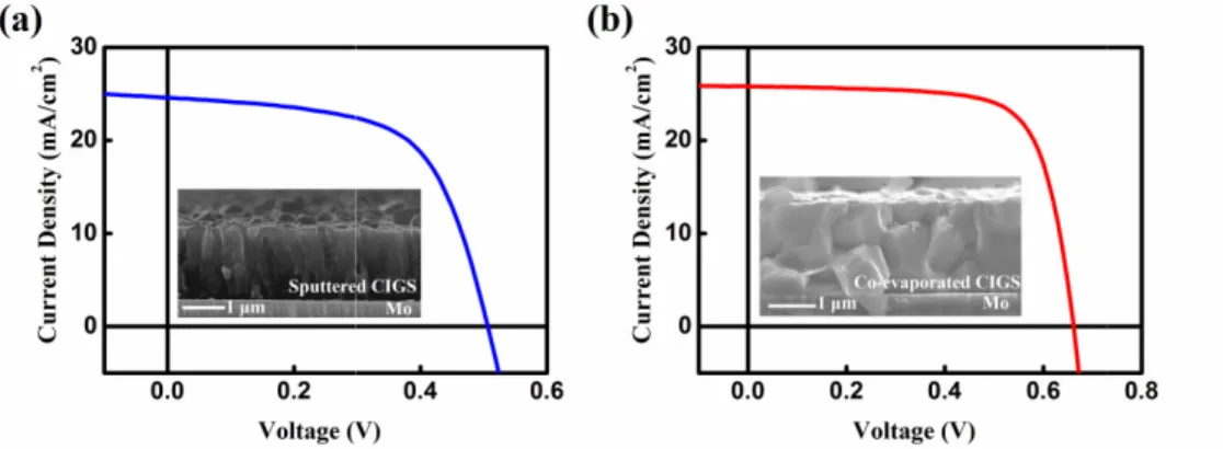
lock-3. I-V characteristics and SEM images Figures 1(a) and 1(b) show the typical I evaporated CIGS samples, res
voltage), JSC (short-circuit current density), filling factor (FF), and solar efficiency ( sputtered and co-evaporated CIGS samples are 0.50 V and 0.66 V, 24.58 mA/cm
mA/cm2, 62% and 72%, and 7.61% and 12.35%, respectively. The results are summarized in Table 1. A lower VOC for the sputtered CIGS is attributed to a smaller bandgap comparing to that of the co-evaporated CIGS, which has been confirmed by photoluminescence spectra (n shown here). Therefore, it was anticipated that the sputtered CIGS films should exhibit a higher JSC than the co-evaporated CIGS films. Nevertheless, an opposite trend was observed. Namely, the JSC of the sputtered CIGS is slightly lower than that of th
One of the possible reasons might be due to a higher defect concentration in the p of the sputtered CIGS that suppresses the
of both CIGS absorption layers. It is evident th
morphologies, with a columnar structure for the sputtered CIGS thin film while that for the co-evaporated CIGS films exhibits a coaxial grain structure. We suspect that columnar grain boundaries of the former m
addition, the lower FF exhibited in the sputtered CIGS comparing to that of the co
CIGS reflects a higher shunt leakage, which is also attributable to the columnar grain structure of the former. It appears that the columnar grain structure may have resulted in a higher concentration of recombination centers for the sputtered CIGS solar cells, which, in turn, yields a lower efficiency of 7.61% as compared to 12.35% obtained for the co
CIGS solar cells.
Fig. 1. I-V characteristics of CIGS solar cells prepared by (a) direct sputtering and (b) co evaporation processes. Insets show the corresponding SEM images of the two samples.
Table 1. The photovoltaic parameters for direct spu
Sputtered Co-evaporated
4. Optical pump-optical probe measurements
In order to further elucidate the possible influences of the grain structure on the microscopic carrier dynamics in these CIGS films, we have carried out systematic OPOP investigations. between the pump and probe pulses. The transient reflectivity change ∆R/R of the probe beam was measured as a function of the pump-probe delay time. The small reflected signals were
-in amplifier. V characteristics and SEM images
show the typical I-V characteristics (IVCs) of the sputtered and co evaporated CIGS samples, respectively. From the IVCs, the obtained VOC (open
circuit current density), filling factor (FF), and solar efficiency (
evaporated CIGS samples are 0.50 V and 0.66 V, 24.58 mA/cm2 and 25.81 and 72%, and 7.61% and 12.35%, respectively. The results are summarized in for the sputtered CIGS is attributed to a smaller bandgap comparing to evaporated CIGS, which has been confirmed by photoluminescence spectra (n shown here). Therefore, it was anticipated that the sputtered CIGS films should exhibit a
evaporated CIGS films. Nevertheless, an opposite trend was observed. of the sputtered CIGS is slightly lower than that of the co-evaporated CIGS. One of the possible reasons might be due to a higher defect concentration in the p-n junction of the sputtered CIGS that suppresses the JSC. The insets show the corresponding SEM images of both CIGS absorption layers. It is evident that the two films display very different grain morphologies, with a columnar structure for the sputtered CIGS thin film while that for the evaporated CIGS films exhibits a coaxial grain structure. We suspect that columnar grain boundaries of the former may have played an important role in suppressing the addition, the lower FF exhibited in the sputtered CIGS comparing to that of the co-evaporated CIGS reflects a higher shunt leakage, which is also attributable to the columnar grain structure e former. It appears that the columnar grain structure may have resulted in a higher concentration of recombination centers for the sputtered CIGS solar cells, which, in turn, yields a lower efficiency of 7.61% as compared to 12.35% obtained for the co-eva
V characteristics of CIGS solar cells prepared by (a) direct sputtering and (b) co-evaporation processes. Insets show the corresponding SEM images of the two samples.
Table 1. The photovoltaic parameters for direct sputtered and co-evaporated CIGS samples
Voc (V) Jsc (mA/cm2) FF (%) η (%)
0.50 24.58 62 7.61
0.66 25.81 72 12.35
optical probe measurements
In order to further elucidate the possible influences of the grain structure on the microscopic carrier dynamics in these CIGS films, we have carried out systematic OPOP investigations. of the probe beam probe delay time. The small reflected signals were
V characteristics (IVCs) of the sputtered and co-(open-circuit
η) for the and 25.81 and 72%, and 7.61% and 12.35%, respectively. The results are summarized in for the sputtered CIGS is attributed to a smaller bandgap comparing to evaporated CIGS, which has been confirmed by photoluminescence spectra (not shown here). Therefore, it was anticipated that the sputtered CIGS films should exhibit a evaporated CIGS films. Nevertheless, an opposite trend was observed. evaporated CIGS. n junction . The insets show the corresponding SEM images at the two films display very different grain morphologies, with a columnar structure for the sputtered CIGS thin film while that for the evaporated CIGS films exhibits a coaxial grain structure. We suspect that columnar grain ay have played an important role in suppressing the JSC. In evaporated CIGS reflects a higher shunt leakage, which is also attributable to the columnar grain structure e former. It appears that the columnar grain structure may have resulted in a higher concentration of recombination centers for the sputtered CIGS solar cells, which, in turn, evaporated
-In order to further elucidate the possible influences of the grain structure on the microscopic carrier dynamics in these CIGS films, we have carried out systematic OPOP investigations.
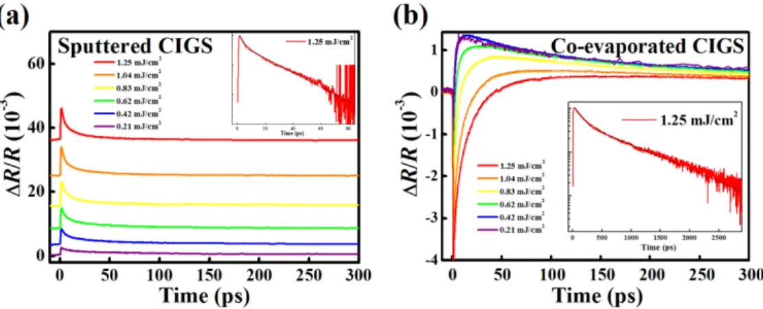
Figures 2(a) and 2(b) show the ∆R/R curves as a function of delay time measured at various pump fluences for sputtered and co-evaporated CIGS samples, respectively. Each ∆R/R curve displayed in Fig. 2(a) can be fitted by a bi-exponential decay while the ∆R/R curves displayed in Fig. 2(b) can be fitted by three exponential decays, including the quick rise of ∆R/R from negative to positive can be fitted by an exponential decay and the sequentially slow decay can be fitted by a bi-exponential decay. We will discuss the dominant relaxation and recombination processes for each sample from the distribution of ∆R/R curves and the fitting results of the carrier-density and pump-fluence dependences of magnitudes and relaxation time constants. As has been pointed out by A. Othonos [9], when the semiconductor is exposed to an ultrafast optical pulse with above band gap photon energy, many processes occur, including the generation of large nonequilibrium carrier densities, elevated carrier temperature, changes in the crystalline structure and band structure. This in turn will affect various macroscopic parameters such as the changes of dielectric constant, reflectivity, and transmission of the material. Moreover, the temporal and spatial evolutions of carrier relaxation and recombination processes are also very complicated. Therefore, the carrier-density, pump-fluence, probe-wavelength, and temperature dependences of the pump-probe results should be accurately analyzed to correctly delineate the mechanisms of ultrafast carrier dynamics prevailing in semiconductors.
Fig. 2. (a) Reflectivity transient for the direct sputtered CIGS films. The inset shows the semi-log plot of the ∆R/R curve for a pump fluence of 1.25 mJ/cm2. The curves were fitted with a biexponential decay function, [A1exp(-t/τfast) + A2exp(-t/τslow)]. Where τfast is the characteristic cooling time of photoexcited hot carriers and τslow is related to carrier recombination. (b) The reflectivity transient for the co-evaporated CIGS films. The negative reflectivity in short delay time is due to the bandgap renormalization effect. The subsequent positive reflectivity transient decay fitted with a biexponential decay is originated from the fast process of the hot phonon relaxation, while the following slow process is due to the defect-related non-radiative recombination.
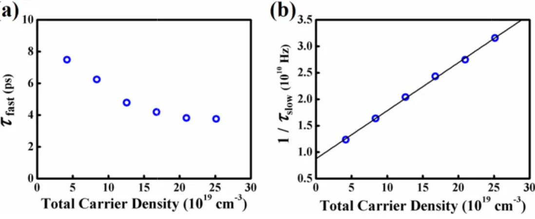
In order to discuss the mechanism of the fast relaxation process for the sputtered CIGS, the fast relaxation time (τfast) versus total carrier density was plotted and displayed in Fig. 3(a). Here we assume that the total carrier density is approximately equal to the photoexcited carrier density since the sputtered CIGS has a carrier density in the range of 1018 ~1019 cm−3 measured by Hall effect measurement, which is smaller than that of photoexcited carriers. For example, a total carrier density of 4.19 × 1019 cm−3
could be generated under a pump fluence of 0.21 mJ/cm2. As shown in Fig. 3(a), τfast decreases from ~7.49 to ~3.76 ps as the total carrier density increases from ~4.19 × 1019 cm−3 to ~2.51 × 1020 cm−3 and reaches the plateau value of ~3.76 ps at the total carrier density larger than ~1.50 × 1020 cm−3
. One of the hot carrier relaxation channels at high electron concentration is that the hot electron energy loss through LO phonon emissions, which is called the hot phonon effect and the screening effect [9]. In this case, the electron relaxation time increases as the excitation density increases.
However, our measurement results obviously do not follow this expectation. This anomalous carrier density dependence is similar to those results reported by Tsai et al. [
hot electron relaxation process in InN and GaAs has been attributed to electron
scattering [11,12]. Therefore, we may conclude that the dominant fast electron relaxation process in the sputtered CIGS films is the electron
In order to interpret the slow relaxation process in the sputtered CIGS, the dependence of slow relaxation rate, 1/τslow, as a function of the total carrier density is shown in
perfect linear fit (solid line) to the data can be obtained using an equation with B0 = 8.74 × 10⁹ s
−1 and
that two recombination mechanisms are involved in the slow relaxation process. The linear carrier density dependence of the recombination rate for the later term
recombination process in degenerated carrier s
suggests the Auger recombination lifetime, which is the order of picosecond magnitudes. It is much faster than the radiative recombination lifetime in the order of
resolved photoluminescence measurements. Another term total carrier density, is associated with the defect
The defect-related non-radiative recombination lifetime,
called Shockley-Read-Hall mechanism at room temperature with
Ndef is the density of defects, carriers [14]. The defect-related non ps.
Fig. 3. (a) The extracted carrier cooling lifetime (
carrier densities in the direct sputtered CIGS film. (b) The 1/ component in the biexponential
sputtered CIGS thin films. In contrast, as shown in
CIGS films, which with much lower free carrier density in the range of
significantly different from those exhibited in sputtered CIGS films. Instead of displaying a steep increase upon pumping (
rapid drop in the initial stage, followed by a quic time. The temporal evolution of
dominated by effects of bandgap renormalization and band filling [ (within 1 ps), the band filling
dominated by the bandgap renormalization effect since the sample carrier density is much lower than that of photoexcited carriers, resulting in an abrupt decrease in
fact that the amplitude of the negative
suggesting a stronger bandgap renormalization effect resulted from a higher photoexcited carrier density at a higher pump fluence. As the carriers cool down and relax to
However, our measurement results obviously do not follow this expectation. This anomalous dence is similar to those results reported by Tsai et al. [10], wherein the hot electron relaxation process in InN and GaAs has been attributed to electron
]. Therefore, we may conclude that the dominant fast electron relaxation rocess in the sputtered CIGS films is the electron-electron scattering.
In order to interpret the slow relaxation process in the sputtered CIGS, the dependence of , as a function of the total carrier density is shown in Fig. 3( perfect linear fit (solid line) to the data can be obtained using an equation1 /
τ
slow = 0+ 2and B2 = 9.09 × 10 −11
cm3 s−1, respectively [10]. This result reveals that two recombination mechanisms are involved in the slow relaxation process. The linear carrier density dependence of the recombination rate for the later term B2n, is due to the Auger recombination process in degenerated carrier system and can be written as 1/τAug [13
suggests the Auger recombination lifetime, which is the order of picosecond magnitudes. It is much faster than the radiative recombination lifetime in the order of µs measured by time
ce measurements. Another term B0, which is independent of the total carrier density, is associated with the defect-related non-radiative recombination process. radiative recombination lifetime, τn, is typically dominated by a so Hall mechanism at room temperature with τn = 1/(Ndefσdefvth
is the density of defects, σdef is their cross section, and vth is the thermal velocity of the related non-radiative recombination lifetime (τn) for this case is ~114
Fig. 3. (a) The extracted carrier cooling lifetime (τfast) in a short delay time under different carrier densities in the direct sputtered CIGS film. (b) The 1/τslow extracted from the slower component in the biexponential decay function used to fit the reflectivity transient of the direct sputtered CIGS thin films.
In contrast, as shown in Fig. 2(b), the carrier relaxation behavior for the co-evaporated CIGS films, which with much lower free carrier density in the range of 1015 ~1016
significantly different from those exhibited in sputtered CIGS films. Instead of displaying a steep increase upon pumping (Fig. 2(a)), each ∆R/R curve displayed in Fig. 2(b) exhibits a rapid drop in the initial stage, followed by a quick rise and then decays slowly with delay time. The temporal evolution of ∆R/R indicates that the carrier relaxation might have been dominated by effects of bandgap renormalization and band filling [15]. At a short delay time (within 1 ps), the band filling is still far from being saturated and the transient reflectance is dominated by the bandgap renormalization effect since the sample carrier density is much lower than that of photoexcited carriers, resulting in an abrupt decrease in ∆R/R signal. The that the amplitude of the negative ∆R/R signal increases with increasing pump fluence, suggesting a stronger bandgap renormalization effect resulted from a higher photoexcited carrier density at a higher pump fluence. As the carriers cool down and relax toward the band However, our measurement results obviously do not follow this expectation. This anomalous ], wherein the hot electron relaxation process in InN and GaAs has been attributed to electron-electron ]. Therefore, we may conclude that the dominant fast electron relaxation In order to interpret the slow relaxation process in the sputtered CIGS, the dependence of Fig. 3(b). A
slow =B0+B n2
]. This result reveals that two recombination mechanisms are involved in the slow relaxation process. The linear , is due to the Auger 13]. The B2 suggests the Auger recombination lifetime, which is the order of picosecond magnitudes. It is
s measured by time-, which is independent of the radiative recombination process. , is typically dominated by a
so-th). Where is the thermal velocity of the ) for this case is ~114
) in a short delay time under different extracted from the slower decay function used to fit the reflectivity transient of the direct
evaporated 16
cm−3, is significantly different from those exhibited in sputtered CIGS films. Instead of displaying a exhibits a k rise and then decays slowly with delay indicates that the carrier relaxation might have been ]. At a short delay time is still far from being saturated and the transient reflectance is dominated by the bandgap renormalization effect since the sample carrier density is much signal. The signal increases with increasing pump fluence, suggesting a stronger bandgap renormalization effect resulted from a higher photoexcited ward the band
edge, the change in absorption by band filling takes over the bandgap renormalization and leads to a sudden increase in reflectivity [
τfast was extracted by fitting the amplitude (A1 < 0), as shown in
evaporated CIGS films is proportional to total carrier density, indicating that the dominant carrier relaxation in this case is
process [9]. Note that the carrier cooling mechanism in the co
different from that in the sputtered CIGS films. The cooling process in the co
CIGS film has eventually brought the amplitude of transient reflectivity back to positive, followed by a biexponational decay (see
relaxation and a defect-related non
analyses, it was observed that the hot phonon relaxation time was increased from 87 ps to 442 ps when the pump fluence was increased from 0.21 mJ/cm
understood as followings. Higher pump fluence is expected to result in a h
temperature, thereby transferring more energy to phonon. As a result, it would take longer time for the phonons to relax back to thermal equilibrium [
biexponential decay is the defect
relaxation time constant, τn, which is largely independent of the total carrier density. Indeed, a constant value of ~750 ps for
densities [15], as shown in
obtained in sputtered CIGS films, which is 114 ps, indicating that the defect recombination rate in the co
sputtered CIGS films. Moreover, no Auger recombination was observed in the co CIGS films, presumably due to a much lower carrier density in the co
Both are consistent with the notion that the columnar grain structure in the sputtered CIGS films is more defective and, hence, exhibits deteriorated conversion efficiency.
Fig. 4. (a) The extracted carrier cooling lifetime ( carrier densities in the co
(τn) as function of the total carrier density for the co 5. Conclusion
In conclusion, the photovoltaic performance of Cu(In,Ga)Se
sputtering and co-evaporation processes were compared, revealing the crucial role played by the resultant film microstructures. Systematic investigations of the ultrafast carrier dynamics in respective films were performed by
measurements. The results demonstrate that the dominant carrier relaxation mechanism strongly depends on the carrier and defect densities in the samples while both can vary dramatically with different depos
edge, the change in absorption by band filling takes over the bandgap renormalization and leads to a sudden increase in reflectivity [15]. To further shed light on band filling effect, the was extracted by fitting the ∆R/R signal to function A1exp(-t/τfast) with a negative
< 0), as shown in Fig. 4(a). It is evident that, the extracted τfast
evaporated CIGS films is proportional to total carrier density, indicating that the dominant carrier relaxation in this case is due to the electron-phonon scattering during the band filling ]. Note that the carrier cooling mechanism in the co-evaporated CIGS films is different from that in the sputtered CIGS films. The cooling process in the co-evaporated ventually brought the amplitude of transient reflectivity back to positive, followed by a biexponational decay (see Fig. 2 inset), which can be attributed to a hot phonon
related non-radiative recombination. By carrying out the fitt analyses, it was observed that the hot phonon relaxation time was increased from 87 ps to 442 ps when the pump fluence was increased from 0.21 mJ/cm2 to 1.25 mJ/cm2. This can be understood as followings. Higher pump fluence is expected to result in a higher electron temperature, thereby transferring more energy to phonon. As a result, it would take longer time for the phonons to relax back to thermal equilibrium [9]. Another contribution to the biexponential decay is the defect-related non-radiative recombination characterized by a , which is largely independent of the total carrier density. Indeed, a constant value of ~750 ps for τn was obtained for the co-evaporated CIGS films at all carrier ], as shown in Fig. 4(b). It is noted that this value is much longer than that obtained in sputtered CIGS films, which is 114 ps, indicating that the defect recombination rate in the co-evaporated CIGS films is significantly lower than that in
reover, no Auger recombination was observed in the co-evaporated CIGS films, presumably due to a much lower carrier density in the co-evaporated CIGS film. Both are consistent with the notion that the columnar grain structure in the sputtered CIGS
more defective and, hence, exhibits deteriorated conversion efficiency.
Fig. 4. (a) The extracted carrier cooling lifetime (τfast) in a short delay time under different carrier densities in the co-evaporated CIGS films. (b) The defect-related recombination lifetime
) as function of the total carrier density for the co-evaporated CIGS films.
In conclusion, the photovoltaic performance of Cu(In,Ga)Se2 thin films prepared by direct evaporation processes were compared, revealing the crucial role played by the resultant film microstructures. Systematic investigations of the ultrafast carrier dynamics in respective films were performed by femtosecond time-resolve pump-probe reflectivity measurements. The results demonstrate that the dominant carrier relaxation mechanism strongly depends on the carrier and defect densities in the samples while both can vary dramatically with different deposition processes. For the direct-sputtered CIGS films, the fast edge, the change in absorption by band filling takes over the bandgap renormalization and ]. To further shed light on band filling effect, the ) with a negative from co-evaporated CIGS films is proportional to total carrier density, indicating that the dominant
phonon scattering during the band filling evaporated CIGS films is evaporated ventually brought the amplitude of transient reflectivity back to positive, inset), which can be attributed to a hot phonon radiative recombination. By carrying out the fitting analyses, it was observed that the hot phonon relaxation time was increased from 87 ps to 442 . This can be igher electron temperature, thereby transferring more energy to phonon. As a result, it would take longer ]. Another contribution to the ombination characterized by a , which is largely independent of the total carrier density. Indeed, a evaporated CIGS films at all carrier . It is noted that this value is much longer than that obtained in sputtered CIGS films, which is 114 ps, indicating that the defect-related evaporated CIGS films is significantly lower than that in evaporated evaporated CIGS film. Both are consistent with the notion that the columnar grain structure in the sputtered CIGS
) in a short delay time under different ion lifetime
thin films prepared by direct evaporation processes were compared, revealing the crucial role played by the resultant film microstructures. Systematic investigations of the ultrafast carrier dynamics probe reflectivity measurements. The results demonstrate that the dominant carrier relaxation mechanism strongly depends on the carrier and defect densities in the samples while both can vary sputtered CIGS films, the fast
relaxation time decreases with the increasing carrier density, which can be attributed to the electron-electron scattering dominated hot carrier relaxation. In contrast, for the co-evaporated CIGS films, the fast dynamics of carrier relaxation is dominated by electron-phonon scattering. On the other hand, the carrier density independent defect-related recombination rate in the co-evaporated CIGS film (τn ~750 ps) is much slower than that obtained from the sputtered CIGS film (τn ~114 ps) and no Auger recombination was observed in the former. These results indicate viable ways for further improving the photovoltaic efficiency of the CIGS-based solar cells as well as optimizing thin film deposition conditions.
Acknowledgments
This research was supported by the National Science Council of Taiwan through grant No. NSC 98-2112-M-009-006-MY3 and National Tsing Hua University through grant No. 100N2024E1. KHW, TK, and JYJ are supported in part by MOE-ATU program operated at NCTU. The authors would also like to thank Compound Semiconductor Solar Cell Department, Next Generation solar cell Division, Green Energy and Environment Research Laboratories, Industrial Technology Research Institute of Taiwan for technical supports.