A Switchable Digital–Analog Low-Dropout
Regulator for Analog Dynamic
Voltage Scaling Technique
Wei-Chung Chen, Student Member, IEEE, Su-Yi Ping, Tzu-Chi Huang, Yu-Huei Lee, Student Member, IEEE,
Ke-Horng Chen, Senior Member, IEEE, and Chin-Long Wey, Fellow, IEEE
Abstract—Dual dynamic voltage scaling (DVS) techniques em-ployed in single-inductor dual-output (SIDO) converters are used to improve the efficiency of the system-on-a-chip (SoC). One DVS technique for digital circuits is controlled by the SoC processor. This paper presents the analog DVS (ADVS) technique for analog circuits to scale voltage across the power MOSFET of the switch-able digital–analog (D/A) low-dropout (LDO) regulator which is the post-regulator cascaded in series with the SIDO converter. The ADVS determines the tradeoff between voltage suppression and ef-ficiency. Furthermore, because of the digital operation of the D/A LDO regulator, the quiescent current is further reduced at light loads while the load current requirement is minimized. In addi-tion, the limitation of the capacitor-free LDO is significantly re-duced by a few microamperes. The test chip was fabricated using a 40-nm CMOS process. Experimental results demonstrated switch-able D/A LDO regulator operation with peak efficiency at 96.7% in analog operation and a 5-mV output voltage ripple at 120-mA load resulting from the advantage of ripple suppression. The power ef-ficiency could be sustained at a value over 92.57% even when the load current decreased to 1 A.
Index Terms—Asynchronous digital low-dropout (LDO) regu-lator, bidirectional asynchronous signal pipeline, dynamic voltage scaling (DVS), hybrid operation, million instructions per second performance, power conversion efficiency, power module, ripple-based control, switching regulator.
I. INTRODUCTION
P
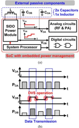
OWER management is an essential system-on-a-chip (SoC) design issue that requires distributive voltage and current levels for distinct subcircuits. SoC power manage-ment requires area efficiency. The single-inductor dual-output (SIDO) converter shown in Fig. 1(a) can power both analog and digital circuits in the SoC by employing two distinct output voltages with only one off-chip inductor [1]–[3] to effectively reduce the print circuit board (PCB) area. Specifically, the volume and cost of manufacturing portable electronics can be reduced.Manuscript received July 25, 2013; revised October 16, 2013; accepted De-cember 23, 2013. Date of publication January 16, 2014; date of current version March 05, 2014. This paper was approved by Associate Editor Gyu-Hyeong Cho.
The authors are with the Institute of Electrical Control Engineering, National Chiao Tung University, Hsinchu 30010, Taiwan (e-mail: khchen@cn.nctu. edu.tw; khchen@faculty.nctu.edu.tw).
Color versions of one or more of the figures in this paper are available online at http://ieeexplore.ieee.org.
Digital Object Identifier 10.1109/JSSC.2013.2297395
Fig. 1. (a) The SoC merges with the integration of SIDO power module, which provides two distinct supply voltages, and , to digital and analog cir-cuits, respectively. (b) Scalable voltage at the corresponding to the SoC operation compared with the fix voltage at the .
Power reduction ability is another necessary feature of power management. Dynamic voltage scaling (DVS) is the most efficient technique for power reduction. Moreover, the system processor can send the voltage indication signal to the SIDO converter to adjust one of two output voltages as one DVS-based power management. The DVS function is generally implemented in digital blocks because digital circuit power consumption is also optimized by the different operation instructions or tasks in SoC [4]–[9].
As shown in Fig. 1(b), if the SoC enters into the data trans-mission operation, the increase of meets the SoC speed requirement. The decrease of also conserves power when the data transmission ends. Comparatively, analog circuits cannot use the similar DVS technique in digital circuits be-cause the supplying voltage for analog circuits should be kept 0018-9200 © 2013 IEEE. Personal use is permitted, but republication/redistribution requires IEEE permission.
CHEN et al.: SWITCHABLE DIGITAL–ANALOG LDO REGULATOR FOR ANALOG DVS TECHNIQUE 741
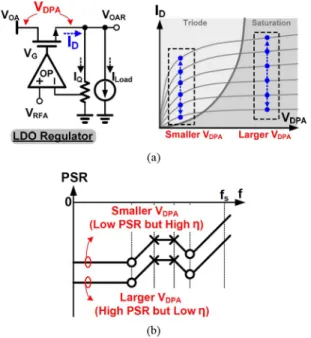
Fig. 2. (a) The dropout voltage of the LDO regulator. (b) The relation-ship between the dropout voltage and the PSRR.
constant to maintain some important performance. In addition, the switching voltage ripple at the will degrade accuracy and power supply rejection ratio (PSRR). Consequently, one low-dropout (LDO) regulator cascaded in series with the SIDO converter is needed to supply voltage to analog circuits with voltage ripples smaller than those at the . Moreover, the improved voltage ripple suppression results in a larger dropout voltage across the pass transistor of the analog LDO regulator because the dropout voltage is considered as a buffer between input supply voltage and output voltage. Fig. 2 illustrates the relationship between dropout voltage and the current across and through the power MOSFET of the analog LDO regulator, respectively.
When the analog LDO regulator operates with smaller dropout voltage, power supply rejection (PSR) negatively escalates alongside the acquisition of higher power efficiency. This condition occurs because the power MOSFET in the triode region rather than the voltage control current source in the deep saturation region exhibits a resistive characteristic. By contrast, larger dropout voltage across the power MOSFET can help improve PSR while simultaneously deteriorating power efficiency. The power MOSDET dissipates large power loss. The new definition of analog-DVS (ADVS) technique for analog circuits is to dynamically scale the dropout voltage according to the loading condition and to maintain constant for analog circuits. In other words, the proposed ADVS technique determines the tradeoff between efficiency and output voltage ripple without affecting the performance of analog circuits in the SoC [10].
Moreover, the LDO regulator design that meets the area effi-ciency demand as a cascading regulator in series with the SIDO converter may require capacitor-free architecture. Thus, sim-ilar to the illustration in Fig. 1, three external passive compo-nents, two capacitors and one inductor, are retained. The em-bedded capacitor-less LDO regulator in the SoC has the
advan-Fig. 3. Analysis of capacitor-free LDO regulator. (a) Frequency response at heavy loads. (b) Frequency response at light loads.
Fig. 4. Unstable phenomena of LDO regulator caused by load current limita-tion in case of heavy-to-light load change of capacitor-free design.
tage of removing the external output capacitor. However, the high quiescent current drastically deteriorates power efficiency compared with the LDO design with the dominant pole compen-sation. The capacitor-free LDO regulator also encounters ob-stacles in stability and restrictions in driving capability. In re-sponse to the disadvantages in the capacitor-free LDO design, the system should dissipate a minimum load current to ensure the stability of light load condition. Generally, 50 to 100 A are required at light loads and further decrease power efficiency.
In this paper, the LDO regulator is cascaded in series with one of the two SIDO converter outputs and designed as a switchable digital–analog (D/A) LDO regulator that supplies analog circuits in the SoC. The advantages are as follows. In the analog operation of the D/A LDO regulator, adjusting the dropout voltage corresponding to the loading condition provides the function of ADVS. Proper dropout voltage is obtained to achieve a regulated output voltage with ripple suppression and power loss reduction. By contrast, digital operation of the D/A LDO regulator reduces the minimum load current requirement to a value near zero [11]. Meanwhile, the dropout voltage is continuously minimized for power optimiza-tion. Therefore, the proposed switchable D/A LDO regulator ensures high efficiency over a wide load range and employs the ADVS technique to supply analog circuits.
In this paper, power management using the dual DVS func-tions for the SoC improves performance in both digital and
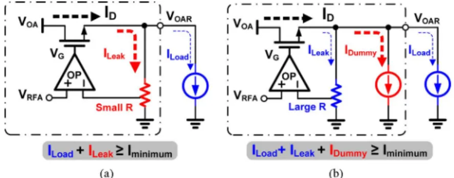
Fig. 5. Conventional solution for alleviating minimum load limitation in the capacitor-free LDO regulator. (a) With an increased quiescent current. (b) With an extra dummy load current.
analog blocks. This paper is organized as follows. The anal-ysis of the analog capacitor-free LDO regulator is discussed in Section II. ADVS function operations with the switchable D/A LDO regulator are examined in Section III. Circuit im-plementations are presented in Section IV. Experimental re-sults are reported in Section V. Finally, conclusions are given in Section VI.
II. ANALYSIS OFANALOGCAPACITOR-FREELDO REGULATOR The analog LDO regulator with Miller compensation is called capacitor-less design. This design has only one small output ca-pacitor to prevent large dip voltage in case of load changes. Thus, the capacitor-less design is more suitable for SoC integra-tion because of the absence of a large output capacitor [12]–[17]. A small integrated output capacitor removes the need for an extra pin for the output capacitor and, thus, has the advantage of reducing volume and cost. However, the bottleneck of the ca-pacitor-free LDO regulator refers to the minimum load current ( ) requirement used to avoid unstable occurrences at light loads. The minimum load current requirement seriously degrades power conversion efficiency at light loads or no load condition.
As shown in Fig. 3, the bandwidth (BW) of the capacitor-free LDO regulator is almost constant over a wide load current range. On-chip Miller compensation generates low-frequency pole and zero, and , respectively. In addition, the high-fre-quency nondominant poles and are located at the gate of the power MOSFET and the output node, respectively. The is dependent on the load current. More specifically, the moves toward lower frequencies because of increased equivalent output resistance resulting from the decreased load current. Once the approaches the , the increasing damping factor seriously deteriorates system stability. From the perspective of the S-domain, the complex poles generate when two non-dominant poles collide with each other and split out of real axis. Even at ultralight loads, the complex poles move to the right half plane (RHP) and cause an unstable oscillation. As shown in Fig. 4, an unexpected phenomenon occurs in cases of different load transient step variations. Output voltage ringing and long settling time ( ) during the transient period are caused by insufficient PM, which result from the complex poles in the capacitor-free LDO regulator.
Even though several techniques in previous literatures pro-pose a decrease in the minimum load current, the minimum load
Fig. 6. Structure of the proposed SIDO power module for dual DVS functions.
current retains tens or hundreds of microamperes [13], [18]. Therefore, efficiency is restricted because of increased leakage current ( ) or dummy load current ( ) payments to meet minimum load current requirements, as shown in Fig. 5 [19]–[22]. Although the ultralight load demands when the SoC system enters into standby mode, the squandered current through power MOSFET remains large and results in substan-tial power loss, as indicated in Fig. 5. The situation shortens the battery usage time for portable devices. Furthermore, without the assistance of an output capacitor in case of load transient periods, good transient response requires a large amount of quiescent current to achieve low impedance and a high slew rate (SR). Thus, current efficiency is poor at light loads if the minimum load current requirement does not decrease.
In order to extend load current to be lower than the min-imum load current defined by conventional capacitor-free LDO regulator, the D/A LDO regulator is switched from the analog operation to the digital operation. Thus, the digitally operating LDO regulator confirms stability under a no-load condition while consuming only 50 nA of quiescent current on the con-troller and only 0.5 A of current on the resistor divider. By contrast, the current flowing through the resistor divider and quiescent current are equal to tens or hundreds of microamperes in the prior arts. In other words, the digital operation in the D/A switchable LDO regulator breaks through the limitations of the minimum load current. In turn, high current efficiency is achieved over a wide load current range with a compact-size solution for SoC power management.
CHEN et al.: SWITCHABLE DIGITAL–ANALOG LDO REGULATOR FOR ANALOG DVS TECHNIQUE 743
Fig. 7. – characteristic of the switchable function in analog operation and digital operation.
III. OPERATION OF THEADVS FUNCTIONWITH THE SWITCHABLED/A LDO REGULATOR
With regard to power management using the dual DVS tech-nique in the SoC, the proposed SIDO power module shown in Fig. 6 has two outputs. One output is for digital circuits and the other, with the switchable D/A LDO regulator, is for analog circuits in the SoC. With only one off-chip inductor, the power stage of the SIDO converter is composed of four power switches from to . These switches transfer the energy from the input battery to both outputs and . The directly supplies digital circuits in the SoC. In DVS operation, the DVS indicator receives the control signal from the system pro-cessor to generate the reference voltage for the . By contrast, the switchable D/A LDO regulator is cascaded in se-ries with the of the SIDO converter to guarantee the supply quality for the analog circuits.
When the D/A LDO regulator is operated using the analog function, the load current condition at the is reflected to the reference adjuster of ADVS modulation to dynamically adjust the dropout voltage, which subsequently leads to voltage ripple suppression or power conservation. If the output load condition at the continuously decreases to an ultralight condition, the switchable D/A LDO regulator is switched to digital opera-tion. Thus, quiescent current decreases because of digital con-troller and dropout voltage is minimized to further enhance the power efficiency. The load-dependent technique indicates the switching procedure between analog and digital operations in the switchable D/A LDO regulator. Therefore, with the feed-back control loop in the SIDO power module, the ADVS and DVS functions are achieved at the and the , respec-tively. The SIDO controller uses the current-programmed con-trol scheme [3] to realize the energy delivery function at the power stage and ensure high power efficiency.
The concept of a switchable D/A LDO regulator is illustrated by the – characteristic in Fig. 7. According to the load
cur-Fig. 8. Operations of both the DVS function for digital circuits and the ADVS function for analog circuits in the proposed SIDO converter.
rent from the SoC power demand, the analog or the digital op-eration is activated to ensure voltage regulation and to achieve high power efficiency. Analog operation uses the ADVS func-tion that adjusts the adaptive dropout voltage through coopera-tion with the SIDO converter.
The – characteristic of power MOSFET is controlled by an error amplifier and shows the parabolic curve between the triode region and the saturation region according to
(1) Under the critical condition in which is equal to , the following equation shows that is proportional to the square of the drain current while neglecting channel length modu-lation parameter :
(2) Consequently, as the load decreases, a smaller dropout voltage is required to ensure proper functioning of the power MOSFET in the saturation region for good voltage ripple suppression. Therefore, small dropout voltage eliminates the superfluous conduction loss on the power MOSFET and en-hances conversion.
Fig. 9. Schematic of the switchable D/A LDO regulator.
At ultralight loads, the pole at the output moves toward the origin and stability decreases drastically. Without the help of the dummy load current, the power MOSFET is modulated by the digital controller rather than the analog controller (the error amplifier) to significantly decrease the quiescent current. Thus, the digital operation of the D/A LDO regulator breaks through the limitations of minimum load current for the capacitor-free LDO regulator. An advantage is that the digital controller fea-tures low quiescent current and further enhances power conver-sion efficiency.
The right-hand side of Fig. 7 illustrates the operating behavior of the power MOSFET in either analog or digital operation. In particular, the error amplifier controls to determine an adequate gate voltage level that corresponds to the load current condition. Moreover, because of the regulated output voltage of the D/A LDO regulator, the load current adjusts the dropout voltage to determine the adequate output voltage of the SIDO converter. When the load condition changes from heavy to light, the changes from to and ob-tains a smaller dropout voltage while simultaneously decreasing the gate voltage level from to for appropriate driving capability. If the load current decreases under certain value, the analog operation switches to digital operation.
During the digital operation, the transistor is divided into several parallel sub-MOSFET units (SMUs). Portions of SMUs are turned on and off by the digital controller according to load current. The number of turn-on SMUs is denoted as . When the load current decreases continuously, the value of shrinks
( in Fig. 7). Thus, the
switch-able D/A LDO regulator uses both analog and digital operation suitable to the demand for analog circuits in the SoC.
Fig. 8 illustrates the operations of both the DVS function for digital circuits and the ADVS function for analog circuits achieved via the switchable D/A LDO regulator. When the SoC enter into operating mode, the DVS function indicated by the system processor is activated to optimize the power consumption. The ADVS function also enables the dynamic adjustment of the dropout voltage of the LDO regulator to guarantee high power conversion efficiency. More specifically, the output voltage level of SIDO power module is adjusted according to the load current condition at the . Moreover, the switchable D/A LDO regulator using the digital operation
Fig. 10. Flowchart of the switchable technique.
once the SoC enters into silent or standby mode. Although the capability of ripple suppression decreases, dropout voltage is reduced to a relatively small value for energy-efficient operation.
IV. CIRCUITIMPLEMENTATION
A. Switchable Digital-or-Analog LDO Regulator
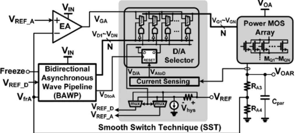
A schematic of the proposed switchable D/A LDO regulator is depicted in Fig. 9 and exhibits the digital and analog opera-tions. These two operations indicate that SMUs are controlled by the bidirectional asynchronous wave pipeline (BAWP) [23] and the error amplifier (EA) [24], respectively. In this case, the smooth switch technique (SST) decides whether digital or analog operation is to be used with respect to load current con-dition. This technique also ensures the continuous and smooth switching procedure between the digital and analog operations. The D/A selector is structured by an array of multiplexers and controlled by the load-dependent signals and . Pass transistors to are controlled by the gate control sig-nals to of the digital controller or the analog signal
CHEN et al.: SWITCHABLE DIGITAL–ANALOG LDO REGULATOR FOR ANALOG DVS TECHNIQUE 745
Fig. 11. Control mechanism of switchable technique between digital operation and analog operation. (a) Switch from digital operation to analog operation. (b) Switch from analog operation to digital operation.
Fig. 12. Schematic of the BAWP circuit in switchable D/A LDO regulator.
Once the analog operation is taken place, the EA generates the error signal that in turn guarantees the output voltage under different output load current conditions. Each gate voltage, from to , of the pass transistors are connected to the error signal when the switchable LDO regulator is in the analog operation. By contrast, the digital operation activates when the SoC enters into silent mode. At this period, the BAWP circuit generates thermometer control codes for each of the pass transistors. The digital control method releases the minimum load limitations at only several microamperes for the system
to effectively conserve power. Moreover, the freeze operation in the BAWP circuit reduces quiescent current to an ultra-low value for high efficiency. Consequently, the proposed switch-able D/A LDO regulator achieves ripple suppression and en-ergy-efficient operation in a distinct mode for high efficiency.
B. Smooth Switch Technique
The proposed switchable D/A LDO regulator indicates only one of two operations that can be enabled in case of load cur-rent change. The SST also ensures the continuous and smooth
takeover procedure between analog and digital operations to prevent undesirable oscillation that induces large output voltage ripples. The hysteresis window adjusts the reference volt-ages of the D/A LDO regulator during the switching dure. The flowchart in Fig. 10 describes the operation proce-dure during switching. When the LDO regulator switches from digital to analog operation during load current increases, the in-creasing value of becomes larger than the pre-defined and triggers the operation procedure by pulse signal . Thus, the EA is activated and the reference voltage of BAWP, , also changes from to the value of ’ - ’. The EA and the BAWP temporarily operate simultaneously. Meanwhile, the EA gradually dominates the control of SMUs when the feedback voltage is larger than . The EA and the BAWP represent the master and the slave, respectively. Finally, the switching procedure is complete when the EA leads the operation and disables the BAWP automatically with reg-ulated output voltage. By contrast, when the LDO regulator switches from analog to digital operation during load current decreases, the decreasing sensing current becomes smaller than the predefined and triggers the switching procedure by the pulse signal , as shown in Fig. 9. The following switching procedure is completed by the aforementioned oppo-site procedure.
The operation waveforms of the SST are shown in Fig. 11. The currents and flow through the SMUs and are controlled by the BAWP and EA, respectively. In cases of increasing load current, the digital operation switches to analog operation as illustrated in Fig. 11(a). At , the
increases with the rising number of turned-on sub-MOSFET units. At , if is larger than , the EA is enabled and the reference voltage of the BAWP, , changes from to the value of - . As a result, the EA and the BAWP function in a master–slave relationship. During this pe-riod, the EA controls the remaining switched-off SMUs and the subsequently increases to regulate the output voltage . Once the feedback voltage increases to a value higher than the at , the is reduced to zero and the BAWP is automatically disabled. Finally, after the recovers at , the switching procedure is complete. The analog operation takes over and enables only the EA. The BAWP shuts down to work in a single loop control.
The analog operation can be switched back to the digital op-eration if the load current decreases to a low enough value, as shown in Fig. 11(b). At , the continuously de-creases and is controlled by the EA. At , once the con-dition of is smaller than , the BAWP is enabled and the reference voltage of EA, , changes from to the value of ’ - ’. Thus, the gradually increases while the is reduced to zero. The switching procedure is complete when the recovers at .
According to the load condition, SMUs are controlled by the analog or digital controller determined by the SST. Ten percent of SMUs are driven by the digital controller at light loads. Ninety percent of SMUs are turned off. During the D/A switching procedure in case of light-to-heavy load changing, the analog controller controls a portion of the power MOS units while the digital controller controls other portions. The analog
Fig. 13. Reference adjuster of ADVS modulation.
Fig. 14. Simulated performance of the switchable D/A LDO regulator.
Fig. 15. Measured load transient with the distinct operation modes in SoC.
controller controls all power MOSFET units at the end of the load change. Finally, none of SMUs are controlled by the digital controller. Consequently, the energy delivered to the output is continuous to retain low output voltage variation. By reflecting the variation of output voltage through the feedback network, the condition of or implies which con-troller is suitable for use. Thus, SMUs are adequately controlled even if the loading condition changes faster than the switching time. Upon setting the reference voltage to – , the sta-bility is confirmed if a moderate or long period is used as the hysteresis window.
C. Bidirectional Asynchronous Wave Pipeline
The BAWP circuit, as illustrated in Fig. 12, generates the control signals for the pass transistors to guarantee the digital operation in the switchable D/A LDO regulator. The digital
CHEN et al.: SWITCHABLE DIGITAL–ANALOG LDO REGULATOR FOR ANALOG DVS TECHNIQUE 747
TABLE I
DESIGNSPECIFICATIONS OFPROPOSEDPOWERMODULE
Fig. 16. Measured digital operation in the switchable D/A LDO regulator.
Fig. 17. Measured analog operation in the switchable D/A LDO regulator.
control unit (DCU) is used to realize the asynchronous oper-ation. The advantage of this condition lies in clock-free op-eration and the reduction of power loss caused by periodical switching. In addition, the header reflector (HR) and the ter-minal reflector (TR) are adopted to ensure correct function in light of the asynchronous operation scheme. The freeze signal interrupts the asynchronous operation once the digital LDO en-ters into static operation. Therefore, current consumption is also minimized and power efficiency is enhanced.
Fig. 18. Measured digital operation in the switchable D/A LDO regulator at ultralight loads.
Fig. 19. Measured voltage ripple on the for analog subcircuits in SoC.
Fig. 20. Measured power efficiency.
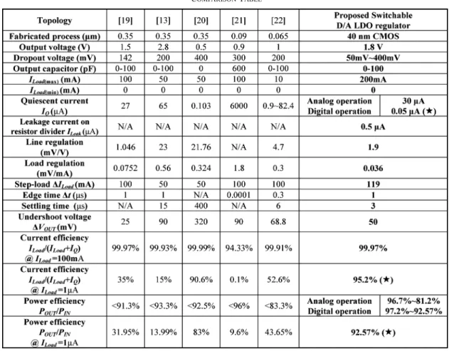
TABLE II COMPARISONTABLE
D. Reference Adjuster of Analog Dynamic Voltage Scaling Modulation
A schematic of the reference adjuster of ADVS modulation is presented in Fig. 13. The current flowing through the pass transistors must be monitored to dynamically adjust the dropout voltage for the analog LDO regulator. The load sensing im-plementation obtains the supply current information through the load sensing circuit. The load current is replicated to the sensed current , to generate the reference voltage by the resistor . Therefore, the load current condition properly modulates the output voltage level of in the SIDO con-verter to guarantee the optimal dropout voltage in the switchable D/A LDO regulator with an analog operation. Furthermore, the minimized indicating voltage also ensures the smallest dropout voltage in the analog LDO regulator.
V. EXPERIMENTALRESULTS
The proposed SIDO converter with the switchable D/A LDO regulator was fabricated using a 40-nm CMOS process. The off-chip inductor for the SIDO power module has a value of 4.7 H and the output capacitors at both and have a value of 4.7 F. The input voltage ranges from 2.7 to 4.2 V. The nominal voltage at the output of the switchable D/A LDO regu-lator is 1.8 V. Fig. 14 illustrates the simulation performance of the switchable D/A LDO regulator. The ADVS works in analog operation at heavy loads and in digital operation at light loads.
Thus, the switchable D/A LDO regulator enhances power con-version efficiency compared with the performance of converters without the ADVS.
Fig. 15 shows the measured load transient response with dis-tinct SoC operation modes. The switchable D/A LDO regulator operates by the digital controller during standby with 1-mA load current. The regulator also operates by the analog controller to suppress the voltage ripple during data transmission opera-tions with 120-mA load current. The detailed design specifica-tions are listed in Table I. If the maximum output capacitance at is 100 pF during the analog operation, the load current can be decreased to 100 A. For safety operation, the opera-tion is switched to digital control when the load current is less than 500 A. Thus, the system is stable even when the load de-creases to 10 A. Fig. 16 presents the measured digital opera-tion in the switchable D/A LDO regulator. The dropout voltage is reduced to 50 mV to minimize energy consumption on the pass transistors. Fig. 17 shows the measured analog operation in switchable D/A LDO regulator with dropout voltage of 240 mV to suppress switching voltage ripples. This condition enhances the supply quality and ensures the operation for noise-sensitive analog subcircuits in the SoC.
Fig. 18 demonstrates the stable system in digital operation even at an ultralight load current of 1 A. Meanwhile, the SIDO converter operates in skip mode to conserve power. Fig. 19 shows the measured the dropout voltage and output voltage rip-ples on the . A 5-mV output voltage ripple is achieved from a 120-mA load current because of the advantage of ripple
CHEN et al.: SWITCHABLE DIGITAL–ANALOG LDO REGULATOR FOR ANALOG DVS TECHNIQUE 749
suppression by the analog operation while LDO voltage is also achieved at ultralight loads for power conservation. The mea-sured power efficiency of switchable D/A LDO is shown in Fig. 20 and indicates the peak efficiency at 96.7% during analog operation. A value higher than 92.57% is retained even when the load current is reduced to 1 A because of digital operation. Fig. 21 shows a chip micrograph with an active silicon area of 2 mm .
Even though prior literature largely emphasized no-load op-eration and adequate performance via high LDO current effi-ciency, as defined by , at values close to 99.9% during heavy loads. There was a need to adequately pro-long battery usage time because portable devices spend much more time in standby mode than in active mode. For complete analysis, power efficiency, defined as and related to quiescent current and dropout voltage at ultralight loads, is eval-uated in comparison with efficiency performance. The compar-ison results on the performance of different LDOs are summa-rized in Table II. Other works consume extra power to increase system stability thereby causing poor power and current effi-ciency at ultralight loads, although they can perform good power and current efficiency at heavy loads. With the D/A switchable technique, the proposed design effectively conserves power at ultralight loads to further extend the battery usage time.
VI. CONCLUSION
This paper presents a SIDO converter with a switchable D/A LDO regulator for improving supply quality. The proposed ADVS function dynamically adjusts the dropout voltage to achieve the tradeoff of ripple suppression function and high efficiency operation. The regulator can switch to digital op-eration once an ultralight load condition occurs. Specifically, the limitations of the minimum load current requirement for the capacitor-free LDO are significantly reduced to several microamperes, and the quiescent current is further reduced to nanoamperes at light loads for power conservation. Further-more, the proposed SST decides a digital or analog operation with respect to the load current condition. The SST ensures the continuous and smooth switching procedure between digital and analog operations. Experimental results demonstrate that the switchable LDO regulator operation exhibits a peak effi-ciency of 96.7% in analog operation and 5-mV output voltage ripple at a load of 120 mA. The efficiency can be maintained at a value over 92.57% even when the load current is at 1 A.
REFERENCES
[1] H.-P. Le, C.-S. Chae, K.-C. Lee, S.-W. Wang, G.-H. Cho, and G.-H. Cho, “A single-inductor switching DC-DC converter with five outputs and ordered power-distributive control,” IEEE J. Solid-State Circuits, vol. 42, no. 12, pp. 2076–2714, Dec. 2007.
[2] Y.-H. Lee, Y.-Y. Yang, S.-J. Wang, K.-H. Chen, Y.-H. Lin, Y.-K. Chen, and C.-C. Huang, “Interleaving energy-conservation mode (IECM) control in single-inductor dual-output (SIDO) step-down converters with 91% peak efficiency,” IEEE J. Solid-State Circuits, vol. 46, no. 4, pp. 904–915, Apr. 2011.
[3] Y.-H. Lee, T.-C. Huang, Y.-Y. Yang, W.-S. Chou, K.-H. Chen, C.-C. Huang, and Y.-H. Lin, “Minimized transient and steady-state cross reg-ulation in 55-nm CMOS single-inductor dual-output (SIDO) step-down DC-DC converter,” IEEE J. Solid-State Circuits, vol. 46, no. 11, pp. 2488–2499, Nov. 2011.
[4] M. E. Sinangil, N. Verma, and A. P. Chandrakasan, “A reconfigurable 8T ultra-dynamic voltage scalable (U-DVS) SRAM in 65 nm CMOS,” IEEE J. Solid-State Circuits, vol. 44, no. 11, pp. 3163–3173, Nov. 2009. [5] Y.-H. Lee, C.-C. Chiu, S.-Y. Peng, K.-H. Chen, Y.-H. Lin, C.-C. Lee, C.-C. Huang, and T.-Y. Tsai, “A near-optimum dynamic voltage scaling (DVS) in 65-nm energy-efficient power management with frequency-based control (FBC) for SoC system,” IEEE J. Solid-State Circuits, vol. 47, no. 11, pp. 2563–2575, Nov. 2012.
[6] W.-S. Chou, T.-C. Huang, Y.-H. Lee, Y.-Y. Yang, Y.-P. Su, K. –H. Chen, C.-C. Huang, Y.-H. Lin, C.-C. Lee, K.-A. Wen, Y.-C. Hsu, Y.-C. Peng, and F.-L. Hsueh, “An embedded dynamic voltage scaling (DVS) system through 55 nm single-inductor dual-output (SIDO) switching converter for 12-bit video digital-to-analog converter,” IEEE J. Solid-State Circuits, vol. 47, no. 7, pp. 1568–1584, Jul. 2012.
[7] Y.-H. Lee, Y.-Y. Yang, K.-H. Chen, Y.-H. Lin, S.-J. Wang, K.-L. Zheng, P.-F. Chen, C.-Y. Hsieh, Y.-Z. Ke, Y.-K. Chen, and C.-C. Huang, “A DVS embedded power management for high efficiency integrated SoC in UWB system,” IEEE J. Solid-State Circuits, vol. 45, no. 11, pp. 2227–2238, Nov. 2010.
[8] S. Das, D. Roberts, S. Lee, S. Pant, D. Blaauw, T. Austin, K. Flautner, and T. Mudge, “A self-tuning DVS processor using delay-error detec-tion and correcdetec-tion,” IEEE J. Solid-State Circuits, vol. 41, no. 4, pp. 792–804, Apr. 2006.
[9] S. Xiao, W. Qiu, G. Miller, T. X. Wu, and I. Batarseh, “An active com-pensator scheme for dynamic voltage scaling of voltage regulators,” IEEE Trans. Power Electron., vol. 24, no. 1, pp. 307–311, Jan. 2009. [10] Y.-H. Lee, W.-C. Chen, C.-C. Chiu, S.-Y. Peng, K.-Y. Chu, K.-H.
Chen, Y.-H. Lin, C.-C. Huang, and C.-C. Lee, “A single-inductor dual-output (SIDO) converter with switchable digital-or-analog low-dropout regulator for ripple suppression and high efficiency operation,” in Proc. IEEE Asian Solid-State Circuits Conf., Nov. 2012, pp. 235–238.
[11] K. Hirairi, Y. Okuma, H. Fuketa, T. Yasufuku, M. Takamiya, M. No-mura, H. Shinohara, and T. Sakurai, “13% power reduction in 16 b integer unit in 40 nm CMOS by adaptive power supply voltage control with parity-based error prediction and detection (PEPD) and fully inte-grated digital LDO,” in IEEE Int. Solid-State Circuits Conf. Dig. Tech. Papers, 2012, pp. 486–487.
[12] Y.-H. Lin, K.-L. Zheng, and K.-H. Chen, “Power MOSFET array for smooth pole tracking in LDO regulator compensation,” IEEE Trans. Power Electron., vol. 23, no. 5, pp. 2421–2427, Sep. 2008.
[13] R. J. Milliken, J. Silva-Martínez, and E. Sanchez-Sinencio, “Full on-chip CMOS low-dropout voltage regulator,” IEEE Trans. Circuits Syst. I, Reg. Papers, vol. 54, no. 9, pp. 1879–1890, Sep. 2007. [14] M. Al-Shyoukh, H. Lee, and R. Perez, “A transient-enhanced
low-qui-escent current low-dropout regulator with buffer impedance attenua-tion,” IEEE J. Solid-State Circuits, vol. 42, no. 8, pp. 1732–1742, Aug. 2007.
[15] P. Y. Or and K. N. Leung, “An output-capacitorless low-dropout regu-lator with direct voltage-spike detection,” IEEE J. Solid-State Circuits, vol. 45, no. 2, pp. 458–466, Feb. 2010.
[16] J. Guo and K. N. Leung, “A 6- W chip-area-efficient output-capacitor-less LDO in 90-nm CMOS technology,” IEEE J. Solid-State Circuits, vol. 45, no. 9, pp. 1896–1905, Sep. 2010.
[17] R. G. Carvajal, J. Ramirez-Angulo, A. J. Lopez-Martin, A. Torralba, J. A. G. Galan, A. Carlosena, and F. M. Chavero, “The flipped voltage fol-lower: A useful cell for low-voltage low-power circuit design,” IEEE Trans. Circuits Syst. I, Reg. Papers, vol. 52, no. 7, pp. 1276–1291, Jul. 2005.
[18] K. Wong and D. Evans, “A 150 mA low noise, high PSRR low-dropout linear regulator in 0.13 m technology for RF SoC applications,” in Proc. IEEE Eur. Solid-State Circuits Conf., 2006, pp. 532–535. [19] C.-M. Chen, T.-W. Tsai, and C.-C. Hung, “Fast transient low-dropout
voltage regulator with hybrid dynamic biasing technique for SoC ap-plication,” IEEE Trans. Very Large Scale Integr. (VLSI) Syst., vol. 21, no. 9, pp. 1742–1747, Sep. 2013.
[20] Y. S. Hwang, M. S. Lin, B. H. Hwang, and J. J. Chen, “A 0.35 m CMOS sub-1 V low-quiescent-current low-dropout regulator,” in Proc. Asian Solid-State Circuits Conf., 2008, pp. 153–156.
[21] P. Hazucha, T. Karnik, B. A. Bradley, C. Parsons, D. Finan, and S. Borkar, “Area-efficient linear regulator with ultra-fast load regulation,” IEEE J. Solid-State Circuits, vol. 40, no. 4, pp. 933–940, Apr. 2005. [22] S. S. Chong and P. K. Chan, “A 0.9- A quiescent current
output-ca-pacitorless LDO regulator with adaptive power transistors in 65-nm CMOS,” IEEE Trans. Circuits Syst. I, Reg. Papers, vol. 60, no. 4, pp. 1072–1081, Apr. 2013.
[23] Y.-H. Lee, S.-Y. Peng, A. C.-H. Wu, C.-C. Chiu, Y.-Y. Yang, M.-H. Huang, K.-H. Chen, Y.-H. Lin, S.-W. Wang, C.-Y. Yeh, C.-C. Huang, and C.-C. Lee, “A 50 nA quiescent current asynchronous digital-LDO with PLL-modulated fast-DVS power management in 40 nm CMOS for 5.6 times MIPS performance,” in Proc. IEEE Symp. VLSI Circuits, 2012, pp. 178–179.
[24] Y.-H. Lee and K.-H. Chen, “A 65 nm sub-1 V multi-stage low-dropout (LDO) regulator design for SoC systems,” in Proc. IEEE Midwest Symp. Circuits and Syst., 2010, pp. 584–587.
Wei-Chung Chen (S’12) was born in Yunlin,
Taiwan. He received the B.S. degree in electrical engineering from National Sun Yat-sen University, Kaohsiung, Taiwan, in 2010, and the M.S. degree from National Chiao Tung University in 2012. He is currently pursuing the Ph.D. degree in the Institute of Electrical and Computer Engineering, National Chiao Tung University, Hsinchu, Taiwan.
He is a member of the Mixed-Signal and Power Management IC Laboratory, Institute of Electrical and Computer Engineering, National Chiao Tung University, Hsinchu, Taiwan. His research interests include the power manage-ment IC design, analog integrated circuits, and mixed-signal IC design.
Yi-Ping Su was born in Taipei, Taiwan. She received
the B.S. degree in electrical engineering from Na-tional Sun Yat-Sen University, Kaohsiung, Taiwan, in 2009. She is currently working toward the Ph.D. degree at the Institute of Electrical Engineering, Na-tional Chiao Tung University, Hsinchu, Taiwan.
She is a Member in the Mixed Signal and Power Management IC Laboratory, Institute of Electrical Engineering, National Chiao Tung University, Hsinchu, Taiwan. Her current research interests include power management and analog integrated circuits design.
Tzu-Chi Huang was born in Hsinchu, Taiwan, in
1983. He received the B.S. and M.S. degrees in elec-trical engineering from National Cheng Kung Uni-versity, Tainan, Taiwan. He is currently working to-ward the Ph.D. degree at the Institute of Electrical Control Engineering, National Chiao Tung Univer-sity, Hsinchu, Taiwan.
He is a member of the Mixed-Signal and Power Management IC Laboratory, National Chiao Tung University, Hsinchu, Taiwan. He is currently working on low-power energy-harvesting sys-tems and power-management circuit design. His research interests include power-management IC design, analog integrated circuits, and mixed-signal IC design.
Yu-Huei Lee (S’09) was born in Taipei, Taiwan. He
received the B.S. and M.S. degrees from National Chiao Tung University, Hsinchu, Taiwan, in 2007 and 2009, respectively, and the Ph.D. degree from the Institute of Electrical Control Engineering, National Chiao Tung University, in 2012.
He is a member of the Mixed Signal and Power IC Laboratory, Institute of Electrical Control Engi-neering, National Chiao Tung University, Hsinchu, Taiwan. His current research interests include power-management IC design, light-emitting diode driver IC design, and analog ICs.
Ke-Horng Chen (M’04–SM’09) received the B.S.,
M.S., and Ph.D. degrees in electrical engineering from National Taiwan University, Taipei, Taiwan, in 1994, 1996, and 2003, respectively.
From 1996 to 1998, he was a part-time IC De-signer with Philips, Taipei, Taiwan. From 1998 to 2000, he was an Application Engineer with Avanti, Ltd., Taiwan. From 2000 to 2003, he was a Project Manager with ACARD, Ltd., where he was engaged in designing power-management ICs. He is currently a Director of the Institute of Electrical Control Engineering and a Professor of the Department of Electrical Engineering, National Chiao Tung University, Hsinchu, Taiwan, where he organized a Mixed-Signal and Power Management IC Laboratory. He is the author or coauthor of more than 100 papers published in journals and conferences and holds several patents. He joined the Editorial Board of Analog Integrated Circuits and Signal Processing in 2013. His current research interests include power-management ICs, mixed-signal circuit designs, display algorithm and driver designs of liquid crystal display (LCD) TV, and red, green, and blue (RGB) color sequential backlight designs.
Dr. Chen has served as an associate editor of the IEEE TRANSACTIONS ON
POWERELECTRONICS, IEEE TRANSACTIONS ONCIRCUITS ANDSYSTEMS—I:
REGULAR PAPERS and the IEEE TRANSACTIONS ON CIRCUITS AND
SYSTEMS—II: EXPRESS BRIEFS. He is on the IEEE Circuits and Systems
(CAS) VLSI Systems and Applications Technical Committee, and the IEEE CAS Power and Energy Circuits and Systems Technical Committee. He joined the Society for Information Display (SID) and International Display Manufacturing Conference (IDMC) Technical Program Sub-committees. He is the Tutorial Co-Chair of the IEEE Asia–Pacific Conference on Circuits and Systems (2012 APCCAS). He is the Tack Chair of Integrated Power Electronics of the IEEE International Conference on Power Electronics and Drive Systems (PEDS) 2013. He is a Technical Program Co-Chair of IEEE International Future Energy Electronics Conference (IFEEC) 2013.
Chin-Long Wey (M’83–SM’97–F’11) received the
Ph.D. degree in electrical engineering from Texas Tech University, Lubbock, TX, USA, in 1983.
He is currently the University Distinguished Professor of Electrical Engineering at National Chiao Tung University (NCTU), Hsinchu, Taiwan. He was the Director General of the National Chip Implementation Center (CIC), Hsinchu, Taiwan, from 2007 to 2010, and the Dean of College of Elec-trical Engineering and Computer Science, National Central University (NCU), during 2003–2006. He came to NCU from Michigan State University, Lansing, MI, USA, where he was a tenured Full Professor of the Electrical and Computer Engineering Department from 1983 to 2003. In 2001, he started up a fab-less design house, JMicron Technology Corporation, Hsinchu, Taiwan, that develops and markets high-speed serial link products. His research interests include design, testing, and fault diagnosis of analog/mixed-signal VLSI circuits and systems, power electronics, power-management systems, and smart battery-management systems.