This content has been downloaded from IOPscience. Please scroll down to see the full text.
Download details:
IP Address: 140.113.38.11
This content was downloaded on 25/04/2014 at 14:49
Please note that terms and conditions apply.
Morphological control of CuPc and its application in organic solar cells
View the table of contents for this issue, or go to the journal homepage for more 2008 Nanotechnology 19 415603
(http://iopscience.iop.org/0957-4484/19/41/415603)
Nanotechnology 19 (2008) 415603 (8pp) doi:10.1088/0957-4484/19/41/415603
Morphological control of CuPc and its
application in organic solar cells
Yu-Sheng Hsiao
1, Wha-Tzong Whang
1,4, Shich-Chang Suen
1,
Jau-Ye Shiu
2and Chih-Ping Chen
31Department of Materials Science and Engineering, National Chiao Tung University,
HsinChu 300, Taiwan, Republic of China
2Center of Applied Sciences, Academia Sinica, Taipei 115, Taiwan, Republic of China 3Materials and Chemical Research Laboratories, Industrial Technology Research Institute,
HsinChu 300, Taiwan, Republic of China E-mail:[email protected]
Received 20 May 2008 Published 4 September 2008
Online atstacks.iop.org/Nano/19/415603 Abstract
We have prepared organic photovoltaic (OPV) cells possessing an ideal bulk heterojunction (BHJ) structure using the self-assembly of copper phthalocyanine (CuPc) as the donor material and fullerene (C60) as the acceptor. The variable self-assembly behavior of CuPc on a diverse
range of substrates (surface energies) allowed us to control the morphology of the interface and the degree of carrier transportation within the active layer. We observed rod-like CuPc
structures on indium–tin oxide (ITO),
poly(3,4-ethylenedioxythiophene)-poly(4-styrenesulfonate) (PEDOT:PSS) and Au substrates. Accordingly, the interfaces and continuing transport path between CuPc and fullerene domains could be greatly improved due to the ideal BHJ structure. In this paper, we discuss the mechanisms of producing CuPc rod-like films on ITO, PEDOT:PSS and Au. The OPV cell performance was greatly enhanced when a mixture of horizontal and vertical CuPc rods was present on the PEDOT:PSS surfaces, i.e. the power conversion efficiency was 50 times greater than that of the corresponding device featuring a planar CuPc structure.
1. Introduction
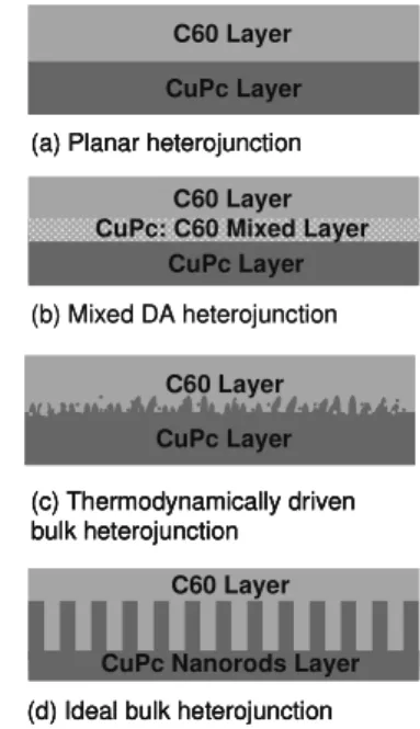
Over the past two decades, organic photovoltaics (OPVs) have received a tremendous amount of attention because of their potential application as green energy devices [1–3]. Indeed, the study of small-molecule solar cells is among the most developed fields of OPVs [4–13]. In conven-tional small-molecule PV systems, the properties of planar heterojunctions (HJs), mixed donor–acceptor (DA) HJs and thermodynamically driven HJs (figures 1(a)–(c)) have been discussed widely [3, 14–16]. In typical planar HJ (bilayer DA) devices, a large degree of photogeneration is sacrificed because of the limited exciton diffusion length (LD): hence, the overall power conversion efficiency (PCE) is limited. The exciton diffusion bottleneck has been overcome through the introduction of bulk HJs through co-deposition of the D and A materials; nevertheless, poor charge transport results in low PCE. Although annealing the DA mixture at high
4 Author to whom any correspondence should be addressed.
temperature to induce phase segregation in the solid state [3] and introducing a DA mixture between D and A layers have been applied successfully to achieve a large DA interface for exciton separation [14–16], the thermodynamically driven random distribution of D and A materials and the limited size of the interfaces for charge transfer can result in inefficient PCE in both of these cases.
Recently, Forrest et al used organic vapor phase deposition (OVPD) to grow copper phthalocyanine (CuPc) nanorods onto ITO substrates to form an OPV possessing an ideal BHJ structure [17–19]. This structure plays a significant role in determining the exciton diffusion efficiency, as illustrated in figure 1(d). The photovoltaic performance of such devices can be improved further when the well-controlled CuPc rods are aligned vertically between the two electrodes; in this case, the quality of the interfaces between the D and A layers could be greatly enhanced, thereby reducing the number of hopping events required for efficient charge transport. For example, a high photocurrent and a low recombination of carriers inside the active layer can be obtained when the diameter of the CuPc
Nanotechnology 19 (2008) 415603 Y-S Hsiao et al
Figure 1. Organic donor–acceptor heterojunctions: (a) planar,
(b) mixed DA, (c) thermodynamically driven bulk and (d) ideal bulk heterojunctions.
rods is controlled within the exciton diffusion length of CuPc (about 10± 3 nm) [4]. Nevertheless, the fabrication and well-defined vertical alignment of CuPc rods remain difficult tasks.
In a previous study, we measured the field emission properties of CuPc nanofibers formed through low-temperature self-assembly, controlling the deposition conditions using a thermal evaporator (TE) [20]. In contrast, other OVPD systems required a high evaporation temperature (>400◦C) and a carrier gas to fabricate the CuPc rod-like films [17–19]. Using these approaches, CuPc nanorods possessing small diameters (<50 nm) and high-quality vertical arrays (ideal BHJ structure) cannot be formed directly. In this paper, we present a simple method for constructing similar CuPc rod-like films using a commercially available TE. The surface energy of the substrate can be modified to control the morphology of the CuPc film at lower evaporation temperatures (<200◦C). Although a number of authors have reported various CuPc morphologies [21, 22], we currently do not have a full understanding of the mechanism of CuPc rod formation. In this study, we used scanning electron microscopy (SEM), grazing incident x-ray diffraction spectroscopy (GIXRD), high-resolution transmission electron microscopy (HRTEM), tapping-mode atomic force microscopy (AFM), x-ray photoelectron spectroscopy (XPS) and contact angle analysis to investigate the growth mechanisms of rod-like CuPc films on Au and PEDOT:PSS films. We obtained highly controllable rod-like CuPc films though the formation of intermolecularπ–π stacking interactions within a TE. We then utilized these morphologically controlled CuPc structures as ideal BHJ structures within OPV devices (figure 1(d)). Herein, we discuss the PV performance of four kinds of HJ structures: planar HJs (PHJ), horizontal rod-based BHJs (h-BHJ), a mixture of horizontal and vertical rod-based BHJs (m-BHJ), and vertical rod-based BHJs (v-BHJ).
2. Experimental details
The donor (D) material used in the devices was copper phthalo-cyanine (CuPc), obtained from Sigma-Aldrich (sublimation grade) without further purification; it was sublimed onto various anodes. The acceptor (A) material was fullerene (C60),
obtained from Sigma-Aldrich (sublimed, 99.9%) and used as received. 2,9-dimethyl-4,7-diphenyl-1,10-phenanthroline (BCP) was purchased from Sigma-Aldrich (99.5%) and used as a exciton blocking layer.
The small-molecule solar cells had the following device structure: anode/CuPc (200 A)/CuPc:C˚ 60 (100 A)/C˚ 60
(300 ˚A)/BCP (75 ˚A)/Al (1500 ˚A). The cells were fabricated on ITO glass (Sanyo) substrates, which were cleaned with organic solvents and a plasma cleaner prior to use. The CuPc films were grown through vacuum sublimation in a thermal evaporator at a base pressure of about 3× 10⁻⁶Torr. CuPc (C32H16CuN8) was sublimed onto various anodes,
including ITO, PEDOT:PSS-coated ITO (PITO) and Au-coated ITO (AITO), from a heated crucible (about 170◦C). The corresponding deposition rates, determined using a quartz crystal microbalance, were about 3 ˚A s−1; the morphologies of the CuPc films were controlled using various substrates at various substrate temperatures (Tsub).
A JEOL JSM-6500F SEM was used to investigate the thickness and morphology of the CuPc films and the cross section of the solar cell devices. The crystalline phase of CuPc films was characterized by GIXRD, using a BEDE D1 system and Cu Kα radiation. The incident angle of the x-ray beam was fixed at 0.5◦. Ultraviolet–visible (UV–vis) spectra were measured using a Perkin-Elmer Lambda 20 UV–vis spectrophotometer. The structures of the CuPc nanorods were imaged and analyzed using a JEOL-2010F high-resolution TEM equipped with an Oxford energy-dispersive spectrometer. Contact angles and surface energies were measured and calculated using the geometric mean approximation (GMA) from the FTA-200 dynamic contact analyzer and two standard liquids: H2O and CH2I2. All devices were treated at 150◦C
for 0.5 h. Current–voltage (I –V ) measurements of the OPV devices were conducted using a computer-controlled Keithley 2400 source measurement unit (SMU) equipped with a Peccell solar simulator (AM 1.5, 100 mW cm−2). The phase diagram of the PEDOT:PSS films was analyzed using a VEECO DICP-II AFM operated in the tapping mode (Si tips on Si cantilevers; spring constant: 2 N m−1; set point: about 0.8–0.9) in air. XPS data were obtained using a VG Scientific Microlab 350 spectrometer operated in the constant-analyzer energy mode (pass energy: 50 eV; excitation source: Mg Kα, 1253.6 eV). XPS measurements were performed at room temperature and at pressures of less than 10−10Torr.
3. Results and discussion
In a previous study [20], we found that the substrate temperature (Tsub) was an important factor controlling the
dimensions and densities of the resulting CuPc nanofibers. When Tsub increased from 100 to 200◦C, the two competitive
phenomena of absorption and desorption affected the 2
Figure 2. SEM images of TE-grown CuPc films on (a) ITO, (b) PITO, (c) AITO (top view) and (d) AITO (side view) substrates. The cartoon
images (a)-1–(c)-1 represent the morphologies in (a)–(c), respectively.
formation of the rod-like CuPc films on these substrates. For instance, we obtained longer, wider, lower density CuPc nanofibers on Au substrates when the value of Tsubwas 200◦C
and the heated crucible temperature was 170◦C, relative to those obtained when Tsubwas 100◦C. In this present study, we
selected a substrate temperature of 100◦C to obtain a higher fiber density of smaller-diameter CuPc nanorods. As use as OPV materials, vertically aligned rod-like structures should allow efficient hole carrier transport by reducing the number of hopping events between CuPc units; we expected high fiber densities and smaller diameters to provide larger interfaces for a high-throughput photocurrent after depositing C60. Figure2
presents top-view SEM images of the CuPc films formed on the ITO, PITO and AITO substrates. We observe that in-plane horizontal CuPc rods (diameter: about 50 nm) formed on ITO (figure 2(a)); a mixture of horizontal and vertical CuPc rods (diameter: about 50 nm) formed on PITO (figure 2(b)) and relatively well-defined vertically arrayed CuPc rods (diameter: < 50 nm) formed on AITO (figure2(c)). Figures1(a)-1–(c)-1 display cartoon representations of the morphologies of the CuPc films formed on the ITO, PITO and AITO substrates, respectively.
The dimensions of vertically arrayed CuPc rods can be optimized to provide improved OPV performance. In this study, we prepared rod-like CuPc films of various lengths by changing the deposition time. The heights of the surface-grown rod-like films were controlled using a quartz crystal microbalance; we chose values of 100, 200, 300 and 500 ˚A, respectively (figures 3(a)–(d)). On the AITO substrate, we observed similar thicknesses for the continuous CuPc films formed under the same conditions (cf figures 3(b) and (c)), suggesting that the growth mechanism may be divided into two steps. In the first step, CuPc tends to form a planar structure (about 40 nm); in the second step, CuPc rods of various lengths grow from the surface of this film. This growth mechanism presumes that the CuPc underlayer presents deposition sites for the formation of the resulting CuPc rods [23]. Figure3(d) reveals that a thicker CuPc continuous film (about 70 nm) formed in the first step and longer CuPc rods in the second. Although the diameters of the CuPc rods (about 25 nm)
Figure 3. SEM images of vertical rod-like CuPc films grown on Au
substrates at thicknesses (measured using a quartz crystal
microbalance) of (a) 100, (b) 200, (c) 300 and (d) 500 ˚A. (e) Cartoon representation of an ideal BHJ of CuPc films. All scale bars are 100 nm.
were independent of the deposition time, their lengths were controllable by changing the deposition time. Figure 3(e) provides a cartoon representation of the surface growth of the CuPc rods; the thickness of the film grown in the first step is represented by the letter T , and the length and diameter of the rods grown in the second step are represented by the letters L and D, respectively. When a thickness of 100 ˚A was selected from the quartz crystal microbalance, the value of L of the vertical CuPc rods was about 25–30 nm with an aspect ratio of about 1–1.2; T was too thin to identify (figure3(a)). The vertical CuPc rods in the 200 ˚A thick sample had rod
Nanotechnology 19 (2008) 415603 Y-S Hsiao et al
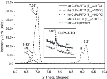
Figure 4. GIXRD spectra of CuPc powders and films deposited on
various substrates at various substrate temperatures: (a) AITO (Tsub= 25◦C), (b) AITO (Tsub= 100◦C), (c) PITO (Tsub= 100◦C),
(d) ITO (Tsub= 100◦C) and (e) CuPc powders.
dimensions ranging from 45 to 90 nm, with an aspect ratio in the range 1.8–3.6 and a value of T of about 35 nm (figure3(b)). In figure3(c), the value of L of the vertical CuPc rods (300 ˚A thick) was about 90–150 nm, with an aspect ratio of about 3.6–6 and a value of T of 35–40 nm. The value of L of the vertical CuPc rods (500 ˚A thick) was about 90–1000 nm with an aspect ratio of about 3.6–40 and a value of T of about 70 nm (figure 3(d)). Consequently, when a thicker CuPc layer was deposited, the length of the CuPc nanorods lacked uniformity and they were poorly vertically arrayed. To produce highly folded DA interfaces with higher exciton diffusion efficiency and fewer defects, we selected the CuPc rods of shorter length and higher vertically arrayed structure in figure3(b) to further investigate their potential PV cell applications.
The two principal phases of CuPc are the so-calledα and β phases [23]. The conductivity of theβ film (2 × 10⁻⁶S m−1) is much lower than that of theα film (2 × 10⁻⁴ S m−1) [24], presumably because the overlap in theπ–π stacking is higher in the α phase than in the β phase. After annealing or depositing at temperatures greater than 200◦C [25], the β-phase CuPc films reveal a 2θ peak at 7.02◦. Figure4presents GIXRD spectra of the CuPc powders and CuPc films formed on the various substrates at values of Tsub of 25 and 100◦C.
By controlling the surface energy of the ITO substrate and varying the value of Tsub, all of the CuPc films could be formed
in the α phase with a signal at a 2θ value at 6.83◦; such high-conductivityα-phase CuPc rod-like films are suitable for mediating exciton transport within OPV devices.
Figure 5(a) presents a top-view SEM image of an Au thin film (about 20 ˚A) on an ITO glass substrate; this film is composed of non-continuous Au nanoparticles (NPs). Figures 5(b)–(d) display TEM images of the CuPc rods deposited on the Au substrates at a value of Tsub of 100◦C;
figure 5(e) presents the corresponding EDX analysis. CuPc rods having a diameter of about 25 nm formed on top of the Au NPs, presumably through crystallization. In our previous study [20], we found that CuPc molecules deposited on either
Figure 5. (a) SEM (top view) image of a thin layer of Au on an ITO
substrate. (b)–(d) TEM images and (e) EDX analysis of CuPc rods deposited on the Au substrates at Tsub= 100◦C. (b) Bottom section
of CuPc rods. (c) CuPc rods. (d) HRTEM images of the upper section of CuPc rods.
Table 1. Effect of substrate on CuPc film morphology. (Note: ITO:
indium–tin oxide glass treated with a plasma cleaner. PITO: PEDOT:PSS films (about 50 nm) coated on ITO. AITO: Au layers (about 20 ˚A) deposited by TE on ITO.)
Substrate Surface energy (mJ m−2) Morphology of CuPc film (Tsub= 100◦C) Diameter of CuPc rods (nm) (Tsub= 100◦C)
ITO 62.62a Horizontal rodsc about 50c
PITO 74.28a Horizontal and
vertical rodsc
about 50c
AITO 39.40a Vertical rodsc about 25c
PEDOT 50.59b Vertical rodsd about 50c
PSS 74.29b Horizontal rodsd about 50c
aThis value was calculated using the geometric mean
approximation (GMA) from the measurements of the advancing contact of H2O and CH2I2.
bThis value was calculated using the equation γ = 0.75(Ecoh/V )2/3[28].
cThe morphology was identified from SEM results.
dThe morphology was presumed from surface energy differences
in the PEDOT:PSS film.
a continuous Au layer (about 250 ˚A) or an Au NP layer (about 20 ˚A) exhibited vertical rod-like structures when Tsub was
100◦C. Our present findings reveal that the surface energy and the temperature of the substrate are two major factors affecting the formation of the various CuPc morphologies (table 1). The variation in morphology that occurred upon increasing the temperature can be explained by considering the following equation [26]:
γ = γ0[1 − (T/T
c)]n (1)
where γ is the surface energy at temperature T and γ0 is
the surface energy at the critical temperature (Tc); the value
of n may be close to unity for anodes. As the temperature increases, substrates having a lower surface energy (e.g. the value ofγ0 for Au is 39.40 mJ m−2) would induce vertical
alignment of CuPc rods, whereas horizontal CuPc rods would grow on high-surface-energy surfaces (e.g. the value of γ0 4
Figure 6. AFM images (topographic (a) and phase (b)) of the PITO
surface. SEM images (top view (c) and estimate (d)) of CuPc rod-like film on the PITO. (e) S(2p) core level spectra of the PITO surface.
for ITO is 62.62 mJ m−2). Although the surface energy of PEDOT:PSS (about 74.28 mJ m−2) is higher than that of ITO, we obtained a mixture of horizontal and vertical CuPc rods. This random distribution of horizontal and vertical rods may have arisen from the inconsistent surface energy of PEDOT:PSS, which is composed of hydrophilic PSS components and hydrophobic PEDOT:PSS domains that undergo nanophase separation, as observed in AFM phase images [27]. To verify the origin of morphological variation of the sample formed on the PEDOT:PSS surface, we calculated the surface energies obtained from cohesive energy density (CED) and XPS analyses and examined AFM and SEM images to distinguish the factors affecting the growth of horizontal and vertical CuPc rods (figure6). The individual surface energies of PEDOT and PSS solid films can exhibit large variations; we estimated the surface energies (γ ) of PEDOT and PSS from the cohesive energy density (CED) values obtained using the empirical equation given by Zisman [28]:
γ = 0.75(CED)2/3 (2)
CED= Ecoh/Vmol. (3)
Table 2 lists the surface energies calculated using equations (2) and (3). The cohesive energies (Ecoh) and
molecular volumes (Vmol) of the various structural groups were
obtained from the literature [29]; the individual groups of PEDOT and PSS are also listed in table 2. Accordingly, we estimated the surface energies of PEDOT and PSS to be 50.59 and 74.29 mJ m−2, respectively, suggesting that out-of-plane CuPc rods would form on PEDOT domains (γ = 50.59 mJ m−2) and in-plane CuPc rods on PSS domains (γ = 74.29 mJ m−2). From contact angle analysis, we found that the surface energy of the PEDOT:PSS film was about 74.28 mJ m−2, close to the value calculated for PSS. This result indicates that traditional contact angle analysis cannot be used alone to determine the effect of the surface energy on the growth of CuPc nanorods. In addition, our findings suggest that variations in the surface energy on the PEDOT:PSS surface were probably responsible for the variations in the CuPc morphology. The topography and phase images of the PEDOT:PSS film (figures 6(a) and (b)) were similar to those reported by Crispin et al [27], with separated PEDOT:PSS and PSS domains. In the phase image, the hard domains appear as bright regions, which we attribute to PEDOT:PSS domains, whereas the dark regions denote the soft segments that belonged to excess PSS domains [27]. The main morphological feature of the PEDOT:PSS film is a homogeneous distribution of the two components on the nanoscale. Figure 6(c) displays a top-view SEM image of the rod-like CuPc film deposited on the PEDOT:PSS film. The distribution of vertical CuPc domains is similar to the distribution of PEDOT:PSS domains in the PSS matrix. Figure6(d) displays a cross-sectional image that we used to provide an estimate of the percentage of vertical CuPc rods (about 13–16%). The XPS analysis also indicates that the atomic percentage of PEDOT was about 15.8% (figure6(e)). The combined results from the AFM, XPS and surface energy analyses suggest that vertical CuPc rods prefer to grow on the surfaces of the PEDOT:PSS domains (PEDOT-rich domains), whereas CuPc tends to form horizontal-rod structures in the PSS domains (PSS-rich domains).
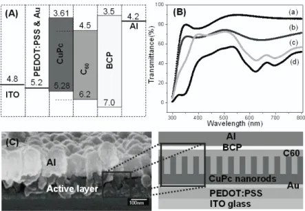
We fabricated OPV cells (glass/anode/CuPc/CuPc:C60/
C60/BCP/Al) [4] featuring ITO (work function(WF) = 4.8 eV),
PEDOT:PSS (WF = 5.2 eV) and Au (WF = 5.2 eV) as
anodes; figure7(A) provides a schematic energy level diagram. In an ideal photovoltaic device, the electrode must have high transparency and the active layer must exhibit high absorption of visible light. Figure 7(B) presents the transmittance behavior of the fully processed solar cells. The absorption of CuPc reaches its maximum at 620 nm; the transmittance of the pristine ITO glass at 620 nm was 83.5% (figure7(B)-a). After a thin Au film (about 20 ˚A) had been deposited, the transmittance at 620 nm of AITO decreased to 65% (figure7(B)-b). After the active layers had been deposited onto AITO (figures7 (B)-c and 7(B)-d), the transmittance in the range 350–800 nm decreased substantially. Figure7(C) presents the architecture and an SEM image of a typical OPV cell. The cross-sectional image of the device clearly reveals the individual layers. The thicknesses of the ITO, PEDOT and Al layers were 190, 50 and 120 nm, respectively. The thickness of the active layer
Nanotechnology 19 (2008) 415603 Y-S Hsiao et al
Figure 7. (A) Schematic representation of the energy levels of the devices. (B) UV–vis spectral transmittance of fully processed solar cells
incorporating various films: (a) ITO, (b) AITO, (c) rod-like CuPc (200 ˚A)/AITO, (d) C60(300 ˚A)/CuPc:C60(1:1) (100 ˚A)/rod-like CuPc
(200 ˚A)/AITO. (C) Cross-sectional image of the device having the structure AITO/CuPc (200 ˚A)/CuPc:C60(100 ˚A)/C60(300 ˚A)/BCP
(75 ˚A)/Al.
Table 2. Calculated values of surface energy for polymers [28,29].
Pristine PEDOT Pristine PSS
Group Ecoh(J mol−1) V (cm3mol−1) Group Ecoh(J mol−1) V (cm3mol−1)
–CH2– 2× (4940) 2× (16.1) –CH2– 1× (4940) 1× (16.1) –O– 2× (3350) 2× (3.8) 1× (3430) 1× (−1.0) Ring closure 5 1× (1050) 1× (16) 1× (31 940) 1× (52.4) Conjugation in ring (double bond) 2× (1670) 2× (−2.2) –SO−3 1× (18 840) 1× (27.6) –S– 1× (14 150) 1× (12.0) γ = 0.75(Ecoh/V )2/3 = 0.75(35 120/63.4)2/3 = 50.59(mJ m−2) γ = 0.75(Ecoh/V )2/3 = 0.75(95 630/97)2/3 = 74.29(mJ m−2) in this cell was about 120 nm; note, however, that it could be
controlled by changing the deposition time.
We conducted comparative experiments (figure8(A)) of OPV devices featuring the various HJ morphologies, including
PHJ (CuPc on ITO or PITO; Tsub = 25◦C), h-BHJ
(CuPc on ITO; Tsub = 100◦C), m-BHJ (CuPc on PITO;
Tsub = 100◦C) and v-BHJ (CuPc on AITO; Tsub =
100◦C). The CuPc morphology was affected by the substrate temperature, with higher values of Tsubdecreasing the surface
energy of a particular substrate, thereby resulting in rod-like films. We constructed the PHJ structure at a value of Tsub
of 25◦C; we obtained the rod-like structures at substrate
temperatures of 100◦C. Figure8(B) reveals the J –V curve characteristics of devices having the configuration anode/CuPc (200 ˚A)/CuPc:C60 (1:1) (100 ˚A)/C60 (300 ˚A)/BCP (75 ˚A)/Al
under illumination at 100 mW cm−2; these devices were all annealed at 150◦C for 30 min prior to testing. In the absence of thermal treatment, the variation of PCE values of devices based on rod-like structures (i.e. h-BHJ, m-BHJ and v-BHJ) was large from different batches. Because many defects existed at the interdigitated DA interfaces, their performance was sacrificed as a result of large interfacial resistances. Table 3 summarizes the performance of each device. The
PHJ devices (a) and (b), which we constructed on CuPc/ITO
Figure 8. (A) Cartoon representations of four types of DA interfaces
in solar cells. (B) J –V curves of devices possessing the configuration anode/CuPc (200 ˚A)/CuPc:C60(1:1) (100 ˚A)/C60(300 ˚A)/BCP
(75 ˚A)/Al under illumination (100 mW cm−2), featuring various CuPc morphologies formed under various annealing temperatures.
Table 3. Performance of CuPc films in photovoltaic cells.
All devices were measured under illumination of AM 1.5 (100 mW cm−2). (Note: PHJ: planar heterojunction structure.
h-BHJ: horizontal-rod-based bulk heterojunction structure. m-BHJ:
mixture of horizontal-and vertical-rod bulk heterojunction structure.
v-BHJ: vertical-rod-based bulk heterojunction structure.)
Device Anode Type of DA structure Jsc (mA cm−2) Voc (V) FF PCE (%) (a) ITO PHJ 0.149 0.338 0.207 0.0104 (b) PITO PHJ 0.0836 0.259 0.194 0.0042 (c) ITO h-BHJ 1.27 0.453 0.275 0.1580 (d) PITO m-BHJ 3.02 0.438 0.386 0.5090 (e) AITO v-BHJ 1.27 0.27 0.215 0.0737
and CuPc/PITO, respectively, performed poorly, as expected. Device (c) possessing the h-BHJ structure exhibited somewhat improved performance. The cell of device (d), incorporating the m-BHJ structure, exhibited the highest value of PCE (0.509%) among this series of devices. Notably, device (e), containing the ideal v-BHJ structure, performed poorly; its value of PCE was lower than that of device (d), primarily because of a remarkable decrease in current density, which we suspect was caused by the different UV–vis spectra of these devices, i.e. the absorption of visible light was reduced by the presence of the Au layer. Thus, although we managed to form the ideal BHJ structure on the Au substrate, there are
some problems that must be solved if it is to perform well in solar cells. Because device (e) exhibited a smaller open-circuit voltage than that of either device (c) or (d), one such issue may be current shunt paths between ITO and CuPc caused by the non-continuous Au NP films [18]. Another issue may be the formation of defects between the interdigitated DA interfaces during this TE process, which would obviously occur to a lesser degree in the h-BHJ and m-BHJ device structures [17]. Therefore, the best performing BHJ solar cell was the m-BHJ device, which we suspect contained a lower number of packing defects and a lower density of vertical CuPc nanorods in the active layer.
4. Conclusion
We have constructed low-molecular-weight organic solar cells using CuPc as the donor and C60as the acceptor and featuring
four types of CuPc morphology. The CuPc morphology could be controlled by varying the surface energy and temperature of the substrates. When using ITO, PITO and AITO as the substrates, the resulting CuPc morphologies were horizontal rods, a mixture of horizontal and vertical rods, and vertically aligned rods, respectively. Thus, substrates possessing lower surface energies (e.g. Au: γ0 = 39.40 mJ m−2) induced
vertical alignment of the CuPc rods, with horizontal CuPc rods forming on high-surface-energy surfaces (e.g. ITO:γ0 =
62.62 mJ m−2). A combination of AFM, XPS and surface energy analyses suggested that vertical CuPc rods preferred to grow on the PEDOT-rich domains of the PITO surface, whereas horizontal CuPc rods formed preferably on its PSS-rich domains. CuPc rods possessing controllable diameters (about 25 nm) and lengths (about 25–1000 nm) were obtained on AITO; they possessed an interdigitated DA structure similar to that of an ideal BHJ solar cell. After thermal annealing the devices at about 150◦C for 30 min, we observed (from GIXRD analysis) no changes in the crystal phases: the CuPc layers maintain the high conductivityα phase through the process. Thus, the values of PCE of CuPc/C60-based solar cells can be
enhanced as a result of the higher degree of folded interfaces upon changing the CuPc structure from planar to horizontal and vertical rods.
Acknowledgments
We thank the National Science Council (project NSC 96-2221-E-009-015) and the Ministry of Economic Affairs, Taiwan, for financial support.
References
[1] Nelson J 2001 Science293 1059
[2] Huynh W U, Dittmer J J and Alivisatos A P 2002 Science
295 2425
[3] Peumans P, Uchida S and Forrest S R 2003 Nature425 158
[4] Peumans P, Yakimov A and Forrest S R 2003 J. Appl. Phys.
93 3693
[5] Djara V and Bern`ede J C 2005 Thin Solid Films493 273
[6] Rand B P, Xue J, Uchida S and Forrest S R 2005 J. Appl. Phys.
Nanotechnology 19 (2008) 415603 Y-S Hsiao et al
[7] Suemori K, Matsumura Y, Yokoyama M and Hiramoto M 2006 Japan. J. Appl. Phys.45 L472
[8] Liu P, Li Q, Huang M, Pan W and Deng W 2006 Appl. Phys. Lett.89 213506
[9] Brovelli F, Rivas B L, Bern`ede J C, del Valle M A, D´ıaz F R and Berredjem Y 2007 Polym. Bull.58 521
[10] Cheynsa D, Gommans H, Odijk M, Poortmans J and Heremans P 2007 Sol. Energy Mater. Sol. Cells91 399
[11] Wong H L, Mak C S K, Chan W K and Djuriˇsic A B 2007 Appl. Phys. Lett.90 081107
[12] Chan M Y, Lai S L, Fung M K, Lee C S and Lee S T 2007 Appl. Phys. Lett.90 023504
[13] Rand B P and Burk D P 2007 Phys. Rev. B75 115327
[14] Peumans P and Forrest S R 2001 Appl. Phys. Lett.79 126
[15] Xue J, Rand B P, Uchida S and Forrest S R 2005 J. Appl. Phys.
98 124903
[16] Schultes S M, Sullivan P, Heutz S, Sanderson B M and Jones T S 2005 Mater. Sci. Eng. C25 858
[17] Yang F, Shtein M and Forrest S R 2005 J. Appl. Phys.
98 124906
[18] Yang F and Forrest S R 2006 Adv. Mater.18 2018
[19] Lunt R R, Benziger J B and Forrest S R 2007 Appl. Phys. Lett.
90 181932
[20] Suen S C, Whang W T, Hou F J and Dai B T 2006 Org. Electron.7 428
[21] Hersam M C, Guisinger N P and Lyding J W 2000 Nanotechnology11 70
[22] Tekiel A, Goryl M and Szymonski M 2007 Nanotechnology
18 475707
[23] Boguslavskii E G, Prokhorova S A and Nadolinnyi V A 2005 J. Struct. Chem.46 1014
[24] Lozzi L, Santucci S, La Rosa S, Delley B and Picozzi S 2004 J. Chem. Phys.121 1883
[25] Karan S and Mallik B 2007 Solid State Commun.143 289
[26] Adamson A W 1990 Physical Chemistry of Surfaces (New York: Wiley)
[27] Crispin X, Jakobsson F L E, Crispin A, Grim P C M, Andersson P, Volodin A, van Haesendonck C, Van der Auweraer M, Salaneck W R and Berggren M 2006 Chem. Mater.18 4354
[28] Zisman W A 1964 Contact angle, wettability and adhesion Advances in Chemistry Series vol 43 (Washington, DC: American Chemical Society)
[29] Van Krevelen D W 1976 Properties of Polymers (Amsterdam: Elsevier) chapters 4 and 8