Y.H. Chen, T.L. Shao, P.C. Liu, and Chih Chena)
National Chiao Tung University, Department of Material Science & Engineering, Hsin-chu 30050, Taiwan
T. Chou
Macronix International Corporation, Ltd., Hsin-chu, 30078, Taiwan
(Received 11 January 2005; accepted 12 May 2005)
Microstructural changes induced by electromigration were studied in eutectic SnAg solder bumps jointed to under-bump metallization (UBM) of Ti/Cr–Cu/Cu and pad metallization of Cu/Ni/Au. Intermetallic compounds (IMCs) and phase transformations were observed during a current stress of 1 × 10⁴A/cm2at 150 °C. On the cathode/ substrate side, some of the (Cuy,Ni1−y)6Sn5transformed into (Nix,Cu1−x)3Sn4due to depletion of Cu atoms caused by the electron flow. It is found that both the cathode/ chip and anode/chip ends could be failure sites. On the cathode/chip side, the UBM dissolved after current stressing for 22 h, and failure may occur due to depletion of solder. On the anode/chip side, a large amount of (Cuy,Ni1−y)6Sn5 or (Nix,Cu1−x)3Sn4 IMCs grew at the low-current-density area due to the migration of Ni and Cu atoms from the substrate side, which may be responsible for the electromigration failure at this end.
I. INTRODUCTION
Flip-chip technology has become one of the most im-portant packaging methods for integrated circuit (IC) packaging. One of its advantages is that a large number of tiny solder bumps can be fabricated into an area array on a chip as input/output (I/O) interconnections. To meet increasing performance requirements, the I/O number keeps increasing. Thus, the size of the bumps shrinks continuously, causing rapid increases in the current den-sity passing through the bumps. Therefore, electromigra-tion (EM) has become an important reliability issue for flip-chip packages.1,2
Furthermore, with increasing environmental concerns, the microelectronics industry is switching to lead-free solder alternatives. One of the most promising candidates is SnAg3.5 solder, because the manufacture of SnAg3.5 solder bumps on a wafer by electrical plating or printing technology is now commercially available. The intercon-nections are established when the solder reacts with the under-bump metallization (UBM) on the chip side and the pad metallization on the substrate side to form inter-metallic compounds (IMCs). However, Pb-free solders are known to have a high reaction rate with Cu or Ni UBM due to their high Sn content of Sn.3Because the
reliability and strength of the solder joint are highly re-lated to IMC formation at the joint, metallurgical reac-tions between solder and metallization layers become an important reliability issue, because the volume ratio of the IMCs to the solder increases as the dimension of the solder bumps decreases. Therefore, the influence of the IMCs on the solder joint reliability has become more critical than before.3
Previous studies on electromigration of flip-chip sol-der bumps focused mainly on eutectic SnPb solsol-ders.4–10 Mean time-to-failure was measured for the eutectic SnPb solder bumps.4A current-crowding effect on the cathode/ chip side was proposed to be responsible for the failure at the cathode/chip side of the SnPb bumps.7–9 Recently, research has focused on electromigration in Pb-free sol-der bumps.11–13For SnAg solder bumps, it was reported that electromigration failure may occur on the anode/chip side.14Chen et al. reported that current stress could en-hance growth or dissolution of the IMCs at the interfaces of Ni and Sn.15However, concerning SnAg3.5 flip-chip solder bumps on Ti/Cr–Cu/Cu UBM and Ni(P)/Au pads, little research has been made on the microstructure evo-lution due to electromigration. This paper investigates microstructural evolution during current stress and its influence on the failure mechanism of electromigration. II. EXPERIMENTAL
The flip-chip packages of SnAg3.5 solder bumps were prepared as follows: The chip size was 9.5 mm × 6.0 mm
a)
Address correspondence to this author. e-mail: [email protected]
with a 105-m UBM diameter. The UBM consisted of 0.7-m Cu, 0.3-m Cr–Cu, and 0.1-m Ti. SnAg3.5 solder paste was printed and deposited on the UBM pad of the chip. The chip was heated in a nitrogen atmosphere oven at the 250 °C peak temperature and remained above the liquidus temperature for approximately 60 s. The bumped die sample was then prepared after sawing.
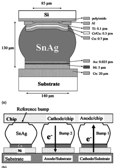
Afterward, the bumped die was mounted on a bisma-leimide triazine (BT) substrate, on which SnAg3.5 solder paste had been printed by metal stenciling on the metal-lized pads of the substrate. The flip-chip sample then was heated again in a nitrogen atmosphere oven at the 250 °C peak temperature for approximately 60 s. The flip-chip joints were formed after the second reflow, and the flip-chip package was then underfilled. The cross-sectional schematic diagram of the flip-chip sample is shown [Fig. 1(a)]. The metallized pad on the substrate consisted of 0.025-m Au, 5-m electroless Ni(P), and 20-m Cu.
Figure 1(b) shows the cross-sectional schematic image of an as-fabricated solder bump. SnAg bump pairs in the package were stressed by a direct current (dc) of 0.59 A at 150 °C, which corresponded to a current den-sity of 1 × 10⁴
A/cm2
. The cross-sectional schematic diagram of the stressing circuit is depicted in Fig. 1(b). The directions of electron flow during electromigration test are indicated by the arrows. In this paper, we denote the right bump as Bump 1, in which the electron flow goes from the substrate side to chip side, and the middle bump as Bump 2, in which the electrons migrate from the chip side to the substrate side. The direction of the elec-tron flow during the current stressing is indicated by the arrows in Fig. 1(b). The calculated current density was based on the contact opening of the chip side, which was 85m in diameter. The contact opening on the substrate side was 140m in diameter, resulting in a smaller current density than that in the chip side. In addition, the reference bump [Fig. 1(b)] went through a similar thermal history without current stress. Thus, it was used to differentiate the morphological change due to thermal aging only.
To observe the microstructure evolution of the eutectic SnAg bumps after current stressing, both cross-sectional and plane-view observations were made. To prepare the plane-view specimens for observation by scanning elec-tron microscope (SEM), samples were ground either from the substrate side or the chip side until there was about 10m of solder left. An etching solution consist-ing of glycerin, nitric acid, and acetic acid at a ratio of 1:1:1 was then used to selectively etch the tin. The reason that we mainly use the plane-view observation herein is stated below. The cross-sectional observation provides only a small portion of the contact opening (a line). How-ever, if we choose plane-view observation, we can ob-serve the IMC distribution in the entire contact opening (an area). Our 3-D simulation can then be used to corre-late the IMC formation and current-crowding effect in the entire contact opening. Therefore, in terms of IMC obser-vation in the contact opening, plane-view images can pro-vide more information than can cross-sectional ones. Thus, the morphology of the IMCs and the entire contact opening could be clearly observed after the selective etching. Mi-crostructure and composition were examined by a JEOL 6500 field emission scanning electron microscope (SEM) and energy-dispersive spectroscopy (EDS), respectively.
To prepare transmission electron microscope (TEM) specimens, a focused ion beam (FIB) was used to cut a thin slice at the failure site or other location of interest. Its dimensions were about 15m × 10 m × 0.1 m, which was prepared for observation in a Philips-Tecnai 20 TEM.
III. RESULTS
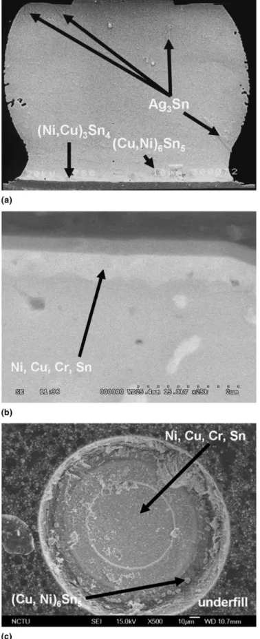
Figure 2(a) shows the cross-sectional SEM image of an as-fabricated SnAg bump. On the substrate side,
FIG. 1. Schematic diagrams of the bumps used in this study. (a) Cross-sectional view showing the structure of a SnAg bump. (b) Schematic diagram of the bumps during current stressing. Direc-tions of electron flow are indicated by arrows.
(Nix,Cu1−x)3Sn4IMCs are observed at the interface of the solder and the Ni metallization, in which the Cu concen-tration was about 10%. In addition, (Cuy,Ni1−y)6Sn5 IMCs with 20% of Ni were also found in the solder near the (Nix,Cu1−x)3Sn4IMCs. The Cu atoms may come from the UBM on the chip side during the second reflow proc-ess.16
On the chip side, sporadic (Cuy,Ni1−y)6Sn5 IMCs with 21% of Ni are found. However, most of the IMCs spalled into the solder, leaving a thin layer of Cr–Cu–Sn on the UBM [Fig. 2(b)]. To observe the contact opening of the chip side more clearly, plane-view observation was feasible after the selective removal of the SnAg solder [Fig. 2(c)]. The inner circle was the UBM that was con-nected to the Al trace in the Si chip. A few IMCs of (Cuy,Ni1−y)6Sn5were found on the periphery of the con-tact, and most of the IMCs in the center region of the contact spalled after the two reflows during the bump-fabrication process. The Ni atoms should come from the substrate side during the second reflow.17
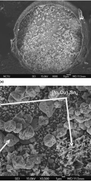
Figure 3(a) shows the plane-view SEM image of the contact opening of the substrate side after the removal of the SnAg solder, in which the morphology of the IMCs formed on the Ni metallization layer can be clearly seen. Figure 3(b) shows the magnified SEM image of the IMCs. Two kinds of IMCs were detected. One is needle-shaped (Nix,Cu1−x)3Sn4with dissolution of 10% of Cu, and the other is block-shaped (Cuy,Ni1−y)6Sn5with 20% of Cu, as indicated by the arrows in the figure. Because the Cu metallization on the BT substrate could not pen-etrate the Ni layer after one reflow, the Cu atoms should migrate from the Cu UBM on the chip side during the reflow for joining the flip-chip package.
Another flip-chip package was stressed by a high-density current for the investigation of microstructural changes. After the current stressing of 1 × 10⁴A/cm2at 150 °C for 20 h, the resistance of the circuit remained unchanged. Therefore, the bumps had not failed when the current was terminated. Figures 4(a) and 4(b) show the cross-sectional SEM images of Bump 1 and Bump 2, respectively. Some cracks were occasionally observed in the periphery of the UBM in the cross-sectioned samples. It is not clear to us how they formed. The cracks occurred at the periphery of the UBM, which was the low-current-density area. Therefore, they may not be attributable to electromigration damage. We speculated that they might be generated during grinding/polishing process. No ob-vious damage was found in either bump after the current stressing. The directions of the electron flow are indi-cated in the figures, in which the electrons drifted from the substrate end to the chip end for Bump 1 and from the chip end to the substrate end for Bump 2. It is in-triguing that a lot of IMCs piled up at the interface of the UBM and the solder, as indicated by one of the arrows in Fig. 4(a). Their composition was determined to be (Nix,Cu1−x)3Sn4with 10% of Cu by EDS. Compared with
FIG. 2. (a) Cross-sectional SEM image of an as-prepared SnAg solder bump. (b) Enlarged SEM image on the interface of the solder and the chip-side UBM in (a). (c) Plane-view SEM image of the chip side without current stressing, in which SnAg3.5 solder has been selec-tively removed, leaving the entire contact opening visible.
the microstructure before stressing in Fig. 2, the forma-tion of these IMCs was triggered by Ni migraforma-tion from the substrate end to the chip end by electromigration. On the other hand, there were no IMCs formed on the chip side of Bump 2, because the electrons migrated atoms from the chip end to the substrate end. Thus, no Ni atoms were detected on the chip end.
To observe the IMCs formed on the chip side more clearly, another flip-chip package was stressed under the same conditions. Afterward, it was ground and polished
from the substrate side, followed by selectively etching of the solder. Thus, the entire contact opening could be observed in plane-view SEM images. The plane-view SEM images of Bump 1 and Bump 2 are shown in Figs. 5(a) and 5(b), respectively. As seen in Fig. 5(a), many (Nix,Cu1−x)3Sn4IMCs with about 10% Cu were found on the contact opening. Occasionally, Ag signals were de-tected on some of the IMCs. Therefore, some Ag3Sn IMCs might have accumulated on these IMCs. For the cathode/chip side as seen in Fig. 5(b), no noticeable Cu– Ni–Sn IMCs were found. Both contacts show no obvious damage after the current stressing.
To investigate the failure mechanism of electromigra-tion for the SnAg bumps, another flip-chip package was stressed at 1 × 10⁴
A/cm2
at 150 °C until open failure
FIG. 3. (a) Plane-view SEM image of the substrate side without ther-mal annealing and current stressing, (b) enlarged image of (a) showing the IMCs formed in the substrate side.
FIG. 4. Cross-sectional SEM images of the chip side after current stress of 1 × 10⁴A/cm2for 20 h: (a) Bump 1; (b) Bump 2. Several (Nix,Cu1−x)3Sn4IMCs formed in the anode/chip side of Bump 1.
occurred. Afterward, the bumps were observed in plan-view SEM images of the chip side and of the board side. It is noteworthy that electromigration failure occurred predominantly at the cathode/chip end for SnPb solder bumps due to void formation at that end.4
Although Hop-kins et al. observed some voids formed on the anode/chip end in SnPb solder, no severe damage was formed in the anode/chip end.10
However, for SnAg solder bumps, we found that the failure may occur at either the cathode/ chip or the anode/chip end at the above stressing condi-tions. Figure 6(a) shows the plane-view SEM image of the failed anode/chip end, in which a large IMC formed at the contact opening, and the UBM was severely de-stroyed. The IMC was analyzed to be (Cuy,Ni1−y)6Sn5
with dissolution of 17% of Ni by SEM EDS. In contrast, the cathode/chip end appeared to be less damaged [Fig. 6(b)]. The IMCs in the contact opening were almost entirely depleted. In some cases, damage occurred in the cathode end or in both ends.14 Although the stressing current density was set to 1 × 10⁴A/cm2, which was the current density when the current distributed uniformly on the entire contact opening, our simulation results showed that the current density inside the solder near the entrance of the Al trace reached 1.8 × 10⁵A/cm2due to the serious current-crowding effect in the joint. Therefore, the current-crowding effect was responsible for the damage at the UBM on the cathode end.
On the other hand, there was no obvious damage found on either the cathode/substrate or anode/substrate ends
FIG. 5. Plane-view SEM images depicting the morphology of the contact openings after the stressing of 1 × 10⁴A/cm2at 150 °C for 20
h: (a) on the anode/chip side; (b) on the cathode/chip side. Dashed lines represent the location where the Al traces are connected to the contact openings.
FIG. 6. Plane-view SEM images on the chip side after stress with a current density of 1 × 10⁴A/cm2at 150 °C for 22 h: (a) anode/chip side; (b) cathode/chip side. A large IMC formed on the anode/chip side.
after the current stressing. This is mainly due to the larger contact opening and thick Cu conducting line on the substrate end, resulting in a smaller current density pass-ing through the contact openpass-ings in the substrate side. The calculated current density was based on the contact opening of the chip side, which was 85m in diameter, whereas the contact opening on the substrate side was 140m in diameter. Nevertheless, phase transformation took place during the current stressing. Figures 7(a) and 7(b) show the plane-view SEM images of the IMCs on the cathode/substrate and the anode/substrate end after the current stressing of 1 × 10⁴A/cm2at 150 °C for 24 h. Open failure occurred in these bump pairs. Compared with the IMCs in Fig. 3(b), most of the (Cuy,Ni1−y)6Sn5 IMCs were transformed into (Nix,Cu1−x)3Sn4. As indi-cated by the arrow in Fig. 7(a), the block-shaped IMCs
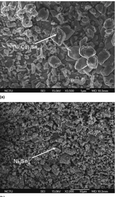
became (Nix,Cu1 − x)3Sn4. In some cases, a few (Cuy,Ni1−y)6Sn5 IMCs were detected inside the solder near the (Nix,Cu1−x)3Sn4 layer. On the anode/substrate end, the IMCs became either Ni3Sn4or (Nix,Cu1−x)3Sn4. In addition, numerous tiny particles were found to be deposited on the surface of the IMC. EDS analysis de-tected a few percent of Ag atoms, which were inferred to be Ag3Sn, that had migrated by electron flow from the solder to the interface of solder and the IMCs.
To separate the thermal effect on the formation of the IMCs during the current stressing, the microstructure of reference bumps was also examined. Figure 8(a) illus-trates the plane-view SEM image of a reference bump after the annealing at 150 °C for 22 h. Compared with the as-fabricated bump in Fig. 2(c), the Ni–Cu–Cr–Sn layer grew thicker after annealing. Figure 8(b) shows the mag-nified SEM image of part of the image in Fig. 8(a), showing the microstructure of the plate-shaped Ni–Cu– Cr–Sn layer, indicating that there are no large Cu–Ni–Sn IMCs formed after annealing. Thus it is believed that the formation of the large IMCs in Figs. 4(a), 5(a), and 6(a) is predominantly due to electromigration. On the other hand, the microstructure on the substrate end did not change much after the annealing, as seen in Figs. 8(c) and 8(d). Similar to the microstructure in Figs. 3(a) and 3(b), both needle-shaped (Nix,Cu1−x)3Sn4 and block-shaped (Cuy,Ni1−y)6Sn5 IMCs were still present after thermal aging, as indicated by the arrows in Fig. 8(d).
To further investigate the IMCs formed due to elec-tromigration and the microstructure near the failure site, a focused ion beam was used to cut thin slices of TEM specimens at significant locations. Figure 9(a) shows the TEM image of the IMCs on the cathode/substrate end after the current stressing of 1 × 10⁴
A/cm2
at 150 °C for 20 h. These bumps failed after the stressing condition. EDS analysis was performed to examine the composition of points B and C, as seen in the figure, and results are displayed in Figs. 9(b) and 9(c), respectively. Grain B consists of Cu, Ni, and Sn elements, which are speculated to be (Nix,Cu1−x)3Sn4,
18
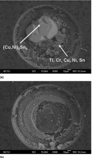
whereas grain C may be Ag3Sn IMC, because it contains Ag, Sn, and Cu elements. Fur-thermore, TEM analysis was used to identify the IMCs on the anode/chip anode side. Figure 10(a) shows the FIB image of a thin slice containing the IMCs on the anode/ chip end from the same bump used in Fig. 9. This slice was located in the center region of the contact opening, and it contained PI, a trace of Al, UBM, and IMCs. The thickness of the IMCs was about 10 m. Figure 10(b) shows the TEM image of the IMCs grown on the UBM, in which grains of the IMC can be clearly seen. EDS results indicated that the IMCs consisted of Sn, Ni, and Cu elements. The diffraction pattern of the grain A in Fig. 10(b) is shown in Fig. 10(c). The IMC was identified as (Cuy,Ni1−y)6Sn5, in which Ni atoms had substituted 14–19% of Cu atoms.
FIG. 7. Plane-view SEM images showing the morphology of the IMCs on the substrate side after stress of 1 × 10⁴A/cm2at 150 °C for
IV. DISCUSSION
The migration of Ni and Cu atoms during current stress plays the key role in the formation and phase trans-formation of IMCs. Three forces drive the migration of Cu and Ni: the gradient of chemical potential, the applied electric field, and the thermal gradient. Unlike electro-migration in Al and Cu, chemical reactions in solder bumps occur during current stress.15It is known that Cu and Sn react at room temperature to form intermetallic Cu6Sn5 compounds.
19–21
Under a gradient of chemical potential, Ni atoms diffuse from the substrate side to the chip side during current stress, while Cu atoms that re-main in the UBM of the chip side tend to diffuse to the substrate side. As seen in Fig. 8(a), there were more Ni atoms in the bump after aging at 150 °C for 22 h without current stress. The concentration gradient of Ni may drive Ni atoms to the chip side. As a rough estimation, the diffusion distance for Ni atoms to diffuse in a matrix of Sn at 150 °C for 22 h is calculated to be 200m.22 Because the bump height is approximately 130m, it is thus reasonable for Ni atoms to diffuse from the substrate side to the chip side after the thermal aging process. However, the solubility of Ni in the eutectic SnAg solder is estimated to be 0.28 at.% at 250 °C.23Therefore, this driving force may be able to migrate few Ni atoms during the electromigration testing. On the other hand, diffusion
of Cu atoms was not obvious. It is speculated that most the Cu atoms had diffused to the substrate side during the second reflow to form (Cuy,Ni1 − y)6Sn5 and (Nix,Cu1−x)3Sn4, because the ternary Cu–Ni–Sn IMCs may possess lower free energy.24 In addition, the Cu atoms remaining in the UBM of the chip side were in-terlocked by the phased-in Cr–Cu layer.2
Moreover, the applied electrical field enhanced the Ni diffusion in Bump 1, while it suppressed the Ni migration in Bump 2. Nickel atoms are found to be very susceptible to electromigration.25 At the anode/chip end, as seen in Figs. 4(a), 5(a), and 6(a), a large amount of Ni atoms migrated by the electron flow to form (Cuy,Ni1−y)6Sn5or (Nix,Cu1−x)3Sn4. In contrast, there are no Ni atoms de-tected at the cathode/chip end. In the same time, the electrons also migrated Cu atoms to the chip end in Bump 1, while they drifted from the cathode/chip end to the anode/substrate end in Bump 2. Three Cu sources that may supply Cu atoms to form (Cuy,Ni1−y)6Sn5 and (Nix,Cu1−x)3Sn4 on the anode/chip end during the cur-rent stressing: (i) the Cu atoms remaining in the UBM, (ii) the Cu atoms in the substrate side, which existed in the form of (Cuy,Ni1−y)6Sn5 or (Nix,Cu1−x)3Sn4, and (iii) Cu metallization under the Ni pad in the BT sub-strate. It is speculated that, in the early stage of electromi-gration, the Cu atoms in the ternary IMCs on the substrate
FIG. 8. Plane-view SEM images showing the morphology of contact openings after the annealing at 150 °C for 22 h: (a) chip side; (b) enlarged image of the Ni–Cu–Cr–Sn layer in (a); (c) substrate side; (d) enlarged image of the IMCs on the substrate side.
FIG. 9. (a) TEM image of the IMC grown on the cathode/chip side after the stressing at the current density of 1 × 10⁴A/cm2at 150 °C for
20 h; (b) corresponding EDS results of point B in (a); (c) correspond-ing EDS results of point C in (a).
FIG. 10. (a) FIB image showing a thin slice containing the IMC around the anode/chip side; (b) TEM image of the IMC grown on the anode/chip end after stressing at the current density of 1 × 10⁴A/cm2
at 150 °C for 20 h; (c) corresponding diffraction pattern of grain A in (b).
side migrated first to the anode/chip side to form (Nix,Cu1−x)3Sn4[Figs. 4(a) and 5(a)]. In some areas, even binary Ni3Sn4IMCs were detected, which meant the Cu atoms in the ternary IMCs were completely exhausted. In addition, the Cu atoms in the UBM of the chip side may be also depleted, causing the deterioration of the contact opening. In the same time, due to the depletion of Cu atoms on the substrate side, some of the (Cuy,Ni1−y)6Sn5 transformed into (Nix,Cu1−x)3Sn4, as observed in Fig. 7(a). On the cathode/chip end in Bump 2, the Cu atoms in the UBM may migrate to the substrate side due to electromigration. Because there were few Cu atoms left in the phased-in layer, the migration of the Cu atoms did not noticeably enrich the Cu concentration in the substrate side. Instead, depletion of Cu atoms in the IMCs near the solder on the substrate side was observed [Fig. 7(b)]. It is hypothesized that some of the Cu atoms had drifted into the (Nix,Cu1−x)3Sn4IMCs.
As current stress continues, the Cu atoms in the met-allization layer of the BT substrate may be driven to the chip side. Tu et al. reported that Cu atoms in the substrate may be able to penetrate a 3-m Ni layer to form Cu– Ni–Sn IMCs in SnAg solder after a few reflows.26 There-fore, it is inferred that the penetration of the Cu atoms may be enhanced by the electron flow. In the earlier stage of electromigration, (Nix,Cu1−x)3Sn4IMCs with approxi-mately 10% of Cu grew first when the Ni and Cu atoms had migrated to the anode/chip side [Figs. 4(a) and 5(a)]. As stressing time increased, more Cu atoms were mi-grated to the anode/chip side, transforming the (Nix,Cu1−x)3Sn4 into (Cuy,Ni1−y)6Sn5 IMCs containing 41% Cu, as (Cuy,Ni1−y)6Sn5is the stable IMC at higher Cu concentration,24
as seen in Fig. 6(a). Nevertheless, in some cases, failure occurs before the phase transforma-tion, leaving the (Nix,Cu1−x)3Sn4 IMCs in the contact.
14
In some failed bumps, part of the Ni metallization was consumed and formed (Cuy,Ni1−y)6Sn5 IMCs there, which is evident for the Cu penetration through the Ni metallization during electromigration.
Three-dimensional simulation on current density has been performed to provide deeper understanding on the relationship between the current crowding phenomenon and the evolution of IMCs. The current density distribu-tion inside the solder near the UBM is shown in Fig. 11. The Al trace in the Si chip connected to the contact from the location depicted by the dashed lines. Therefore, cur-rent crowding occurred at the junction of the Al trace and the contact opening. The current density at the vicinity of the entrance into the solder bump is as high as 1.3 × 10⁵ A/cm2when 0.59 A was applied, whereas it is less than 1 × 10³A/cm2for the contact opening far from the en-trance point. This current density distribution may affect the formation of IMCs during current stressing. As shown in Fig. 5(b), it is clear that the IMCs at the vicinity of the entrance point appeared much less often than in the
rest of the contact opening. As this is the cathode/chip side, the IMCs/UBM may dissolute during electromigra-tion, with dissolution becoming faster at areas with high current density. On the other hand, the effect of current crowding on IMCs formation on the anode/chip side is quite different. The high-current-density area for the anode/chip side was approximately at the similar loca-tion. However, less (Nix,Cu1−x)3Sn4IMCs formed at the entrance point of the contact, and more IMCs accumu-lated at the low-current-density region [Fig. 5(a)]. In ad-dition, a large (Cuy,Ni1−y)6Sn5 IMC formed at the low-current-density region [Fig. 6(b)]. Tu et al. proposed that resistive particles tend to move to low-current-density region to lower energy.27The resistivities for the SnAg solder, Ni3Sn4IMC, and Cu6Sn5IMC are 12.3, 28.5, and 17.5, respectively. Thus, compared to the SnAg solder, the (Nix,Cu1−x)3Sn4and (Cuy,Ni1−y)6Sn5IMCs are more resistive. Therefore, the IMCs may prefer to form at low-current-density regions.
The thermal gradient may also affect the migration of atoms. Ye et al. proposed that the thermal gradient in-duced by the electrical field may migrate Sn atoms from the chip side to the substrate side, causing void formation in the chip side.10 This is denoted as thermomigration (TM) in this paper. It may also enhance the migration of the Cu atoms to the substrate side. However, this gradient may inhibit the diffusion of Ni atoms. Because many Cu–Ni–Sn IMCs formed in the anode/chip side during electromigration, it is inferred that the effect of the elec-tric field dominates the diffusion of Cu and Ni atoms and that the thermal gradient has little contribution to the migration of Cu and Ni atoms.
It is intriguing that the SnAg bumps may fail at the cathode/chip side under the above stress conditions. Jang
FIG. 11. Three-dimensional simulation of current-density distribution for solder near the contact opening of the chip side.
et al. also found a large Ni–Cu–Sn IMC in the bulk SnAg solder bumps when they were stressed at 3.58 × 10⁴A/cm2at 140 °C.11However, the SnAg bumps failed at the cathode/chip side. In our study, 60% of the stressed bump pairs were found to fail at the cathode/chip side (9 out of 15). Although the anode/chip side did not fail for these bump pairs, Ni–Cu–Sn IMC was observed to grow at the interface of the UBM and the solder after current stress. It is speculated that the formation of the large ternary Cu–Ni–Sn IMCs may accompany volume expan-sion, generating stress around the UBM on the anode/ chip side. Cracks might be initiated and propagated as the stress increases due to the growth of the IMC, resulting in a smaller contact area. Thus, open failure occurs as the contact is destroyed.
Compared to Pb-bearing SnPb solders, no obvious for-mation of IMCs was reported during current stressing because the addition of Pb is known to effectively reduce the reactivity between Sn and Cu or Ni. In addition, at stress temperatures higher than 120 °C, Pb atoms are the migrating species and accumulate at the interface of the UBM and the solder on the chip side, preventing the formation of IMCs.1 Therefore, it is inferred that three failure mechanisms compete during current stress-ing of solder bumps: EM-induced void formation on the cathode/chip side,4,6–9,11,12 TM-induced void formation on the anode/chip side,10 and EM-induced IMC forma-tion on the anode/chip side in this study.14 For eutectic SnPb solder bumps, the concentration of Sn is only 63%, and Pb atoms are accumulated on the anode/chip side to inhabit Cu–Ni–Sn IMC formation. Thus, either EM-induced void formation or TM-EM-induced void formation prevails in the SnPb system. For the SnAg solder bumps, the 96.5% content of Sn may facilitate the formation of the Cu–Ni–Sn IMC. Therefore, the mechanism of EM-induced IMC formation may occur in the SnAg3.5 sys-tem under the present stress conditions. In addition, ac-cording to Ye et al., the higher current density on the chip side also causes more serious joule heating, which accel-erates the growth of the IMC. This unique failure mode may play a very important role in the electromigration of Pb-free solders under stringent stress conditions, because most of the Pb-free solders contain over 95% Sn, and a Ni/Cu pad is the most popular metallization on the sub-strate side.
The stress conditions may also affect the failure mechanism in the SnAg solder bumps. Our previous study showed that failure occurred at cathode/chip when the bumps were stressed at 5 × 10³A/cm2at 150 °C. No IMC formation was found in the anode/chip side after the stressing for 192 h.14 However, as the dimension of the solder bumps keep shrinking and the required cur-rent that each bump needs to carry keep increasing, the EM testing condition might approach 1 × 10⁴A/cm2at 150 °C. The failure mechanism of EM-induced IMC
formation may emerge as an important issue. Yet, tem-perature effect is not clear at this moment. It is speculated that higher temperatures may facilitate the diffusion of Ni and Cu from the substrate to the chip side. Thus, failure may occur in the anode/chip side.
V. CONCLUSIONS
In summary, the electromigration damage on the SnAg3.5 solder bumps of a flip-chip package has been investigated at the current density of 1 × 10⁴ A/cm2 at 150 °C. Open failure may occur in the anode/chip side. Microstructural evolution during electromigration has been examined. During the early stage of electromi-gration, part of the UBM on the cathode/chip side dis-solved, and (Nix,Cu1−x)3Sn4 IMCs formed at the low-current-density location on the anode/chip side. As cur-rent stressing continued, they may transformed into (Cuy,Ni1−y)6Sn5IMCs, which may be responsible for the electromigration failure in the anode/chip side. On the substrate side, phase transformation was observed. Yet, no failure occurred in the substrate side.
ACKNOWLEDGMENTS
The authors thank the National Science Council of R.O.C. for the financial support of this study through Grant No. 90-2216-E-009-042 and Professor K.N. Tu at UCLA for helpful discussions.
REFERENCES
1. K.N. Tu: Recent advances on electromigration in very-large-scale-integration of interconnects. J. Appl. Phys. 94, 5451 (2003). 2. K.N. Tu and K. Zeng: Sn–Pb solder reaction in flip chip
technol-ogy. Mater. Sci. Eng. Rep. R34, 1 (2001).
3. K. Zeng and K.N. Tu: Six cases of reliability study of Pb-free solder joints in electronic packaging technology. Mater. Sci. Eng. Rep. R38, 55 (2002).
4. S. Brandenburg and S. Yeh: Electromigration studies of flip chip bump solder joints. Proceedings of the Surface Mount Interna-tional Conference and Exhibition, Integrated Electronics Engi-neering Center (IEEC), San Jose, CA (1998). p. 337.
5. C.Y. Liu, C. Chen, C.N. Liao, and K.N. Tu: Microstructure– electromigration correlation in a thin stripe of eutectic SnPb solder stressed between Cu electrodes. Appl. Phys. Lett. 75, 58 (1999). 6. J.D. Wu, P.J. Zheng, K. Lee, C.T. Chiu, and J.J. Lee:
Electromi-gration failures of UBM/bump systems of flip-chip packages. Pro-ceedings of the 52nd Electronic Components and Technology Conference, IEEE Components, Packaging, and Manufacturing Technology Society, San Diego, CA (2002). p. 452.
7. E.C.C. Yeh, W.J. Choi, and K.N. Tu: Current-crowding-induced electromigration failure in flip chip solder joints. Appl. Phys. Lett.
80(4), 580 (2002).
8. J.W. Nah, K.W. Paik, and J.O. Suh: Mechanism of electromigration-induced failure in the 97Pb–3Sn and 37Pb–63Sn composite solder joints. J. Appl. Phys. 94(12), 7560 (2003).
during electromigration eutectic SnPb solder bumps. J. Mater. Res. 19(8), 2394 (2004).
10. H. Ye, C. Basaran, and D. Hopkins: Thermomigration in Pb-Sn solder joints under joule heating during electric current stressing. Appl. Phys. Lett. 82(7), 1045 (2003).
11. T.Y. Lee, K.N. Tu, and D.R. Frear: Electromigration of eutectic SnPb and SnAg3.8Cu0.7 flip-chip solder bumps and under-bump metallization. J. Appl. Phys. 90(9), 4502 (2001).
12. S.Y. Jang, J. Wolf, W.S. Kwon, and K.W. Paik: UBM (under bump metallization) study for Pb-free electroplating bumping: In-terface reaction, and electromigration. Electronic Components and Technology Conference, Packaging, and Manufacturing Technol-ogy Society, IEEE Components, IEEE, San Diego, CA (2002). p. 1213.
13. W.J. Choi, E.C.C. Yeh, and K.N. Tu: Mean-time-to-failure study of flip-chip solder joints on Cu/Ni(V)/Al thin-film under-bump-metallization. J. Appl. Phys. 94(9), 5665 (2003).
14. T.L. Shao, Y.H. Chen, S.H. Chiu, and C. Chen: Electromigration failure mechanisms for SnAg3.5 solder bumps on Ti/Cr–Cu/Cu and Ni(P)/Au metallization pads. J. Appl. Phys. 96(8), 4518 (2004).
15. S.W. Chen, C.M. Chen, and W.C. Liu: Electric current effects upon the Sn/Cu and Sn/Ni interfacial reactions. J. Electron. Mater.
27(11), 1193 (1998).
16. S.J. Wang and C.Y. Liu: Study of interaction between Cu–Sn and Ni–Sn interfacial reactions by Ni–Sn3.5Ag–Cu sandwich struc-ture. J. Electron. Mater. 32(11), 1303 (2003).
17. T.L. Shao, T.S. Chen, Y.M. Huang, and C. Chen: Cross interac-tions on interfacial reacinterac-tions of solder bumps and metallization layers during reflow. J. Mater. Res. 19(12), 3654 (2004).
18. P.G. Kim, J.W. Jang, T.Y. Lee, and K.N. Tu: Interfacial reaction and wetting behavior in eutectic SnPb solder on Ni/Ti thin films and Ni foils. J. Appl. Phys. 86(12), 6746 (1999).
19. K.N. Tu: Interdiffusion and reaction in bimetallic Cu–Sn thin films. Acta Metall. 21(4), 347 (1973).
20. J.W. Mayer, J.M. Poate, and K.N. Tu: Thin films and solid-phase reactions. Science 190, 228 (1975).
21. K.N. Tu and R.D. Thompson: Kinetics of interfacial reaction in bimetallic Cu–Sn thin films. Acta Mater. 30, 947 (1982). 22. H. Mehrer: Reference Database for Diffusivities,
Landolt-Börnstein New Series (Springer, Berlin, 1990), Group III, Vol. 26. 23. K. Zeng and J. Kivilahti: Thermodynamic Calculation of Satura-tion Solubilities of Some Metals in Pb-Free Solders. Internal Re-port (Helsinki University of Technology, Helsinki, Finland, 2000).
24. W.T. Chen, C.E. Ho, and C.R. Kao: Effect of concentration on the interfacial reactions between Ni and Sn–Cu solders. J. Mater. Res.
17(2), 263 (2002).
25. S.N. Mei, J. Shi, and H.B. Huntington: Diffusion and electromi-gration in lead alloys. I. Nickel as a mobile element. J. Appl. Phys.
62(2), 444 (1987).
26. C.S. Huang, J.G. Duh, and Y.M. Chen: Metallurgical reaction of the Sn–3.5Ag solder and Sn–37Pb solder with Ni/Cu under-bump metallization in a flip-chip package. J. Electron. Mater. 32(12), 1509 (2003).
27. K.N. Tu, C.C. Yeh, and C.Y. Liu: Effect of current crowding on vacancy diffusion and void formation in electromigration. Appl. Phys. Lett. 76(8), 988 (2000).