Fast Transient (FT) Technique With Adaptive
Phase Margin (APM) for Current Mode
DC-DC Buck Converters
Yu-Huei Lee, Student Member, IEEE, Shao-Chang Huang, Shih-Wei Wang, and
Ke-Horng Chen, Senior Member, IEEE
Abstract—This paper proposes a fast transient (FT) control with the adaptive phase margin (APM) to achieve good transient re-sponse in current-mode DC-DC buck converters at different load conditions. The overshoot/undershoot voltage and the transient re-covery time are effectively reduced. The APM control can always maintain the system phase margin at an adequate value under dif-ferent load conditions. That is, the compensation pole-zero pair is adapted to load current to extend the system bandwidth and get an adequate phase margin. Experimental results show the over-shoot/undershoot voltage is smaller than 60 mV (3%) and transient period is smaller than 12 s as load current suddenly changes from 100 to 500 mA, or vice versa. Compared with conventional designs without any fast transient technique, the undershoot voltage and recovery time are enhanced by 45% and 85%, respectively.
Index Terms—Adaptive phase margin (APM), fast transient (FT), loop bandwidth, pole-zero cancellation, stability.
I. INTRODUCTION
H
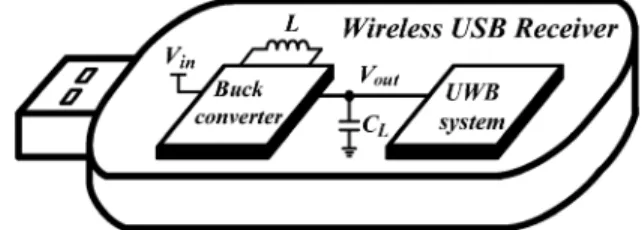
IGH-QUALITY power management converters are de-manded for portable devices such as cell phones, dig-ital cameras, and other multimedia equipment. Voltage regu-lation and transient recovery time are treated as the important issues in providing a good power supply. The reason for the demand in high-quality power supply converters is that the un-stable supply voltage in case of load variations may cause ab-normal operation or deteriorate the performance of the portable devices. Among the applications like system-on-chip (SoC) and the motherboard, a stable power management, which features in the high-quality power supply, fast line/load transient response, and high power conversion efficiency, is the trend to increase the competitiveness of the portable products [1]. Therefore, the good transient response is the design consideration in DC-DC converter that is necessary for today’s power management ap-plication.Despite these challenges and the special design techniques, wireless USB receiver, which includes the power management module and the ultra-wide band (UWB) system as shown in Fig. 1, provides an ideal solution for wireless internet or some
Manuscript received January 13, 2011; revised May 12, 2011; accepted July 18, 2011. Date of publication August 30, 2011; date of current version July 19, 2012. This work was also supported by the National Science Council, Taiwan, under Grant NSC 100-2220-E-009-050 and Grant NSC 100-2220-E-009-055.
The authors are with the Institute of Electrical Control Engineering, National Chiao Tung University, Hsinchu 300, Taiwan (e-mail: khchen@cn.nctu.edu.tw). Color versions of one or more of the figures in this paper are available online at http://ieeexplore.ieee.org.
Digital Object Identifier 10.1109/TVLSI.2011.2163093
Fig. 1. Main structure of the wireless USB receiver.
Fig. 2. Supply voltage variation under the different power request condition in UWB systems.
battery-operated portable applications. This structure allows the UWB protocol to support multiple low-power modes and data transmission. In the UWB system, if the throughput constraint is cycling between different operating modes, the power request is also changed in order to meet the supply power of different mode operations. When the UWB system enters into the data transmission period, the power request would increase suddenly that has a consequence of supply voltage variation. As depicted in Fig. 2, undershoot and overshoot voltages appear at the mo-ment of mode transmission. The large dip supply voltage and the long voltage recovery time have a serious influence on the per-formance of UWB systems. Consequently, a high-quality power source is always an essential demand in the power management module design.
Several techniques are claimed to improve the transient response for getting a reliable supply voltage in DC-DC converters [2]–[10]. Some literatures in today’s fast transient techniques are focused on speeding up the charging or dis-charging time for the large compensation capacitor [2], [3]. Thus, a large driving current is sourcing or sinking into the com-pensation capacitor when the load current changes. A careful design consideration of the system stability is needed to ensure a stable operation. The adaptive compensation in literature [5]
large output voltage ripple would affect the performance of the noise-sensitive circuit. Additionally, the current-mode control needs the slope compensation signal to avoid the sub-harmonic oscillation. The slope compensation signal independent of input and output can ensure a wide load range operation but has less help in accelerating the transient response [7]. The digital control methods [11]–[13] are also a wide-used mechanism in DC-DC converter for getting fast response. However, deterio-rated performance and high cost are derived from the function of analog-to-digital converter. Moreover, there are different control methods in DC-DC buck converters [14]–[18]. These different control schemes achieve the good transient response but increases the design complexity.
In this paper, a fast transient with adaptive phase margin (APM) control is proposed in the current-mode DC-DC buck converters. The conventional compensation technique in DC-DC buck converters is presented in Section II. Fast transient control procedure with proposed APM is illus-trated in Section III. Circuit implementations are described in Section IV. Experimental results are shown in Section V. Finally, a conclusion is made in Section VI.
II. COMPENSATIONTECHNIQUES INVOLTAGE-MODE AND
CURRENT-MODEDC-DC BUCKCONVERTERS
There are some different design issue of compensation tech-niques between voltage and current mode DC-DC buck con-verters. Voltage-mode buck converter needs proportional-inte-gral-differential (PID) compensator due to the LC dual poles, and , as illustrated in Fig. 3(a) and the frequency re-sponse depicted in Fig. 3(b). The transfer function of the power stage is written as (1). The usage of a PID compensator in voltage-mode buck converters can enhance low-frequency gain and phase margin (PM). The PID compensator generates three
compensation and the need of many external passive compo-nents is the major disadvantage in the design of voltage-mode buck converters, as shown in (1)–(3) at the bottom of the page.
The compensation scheme of the current-mode buck con-verter is simpler than that of the voltage-mode control owing to the single pole at the power stage. That is, the proportional-integral (PI) compensator with a pole-zero pair is eligible to achieve system compensation. The compensation zero is usually used to cancel the load-dependent system pole lo-cated at the output. However, the position of would affect the performance of the current-mode buck converter under the different load condition. The PI compensator, which generates a fixed compensation pole-zero pair, can ensure the system sta-bility but cannot ensure a good transient response at any load conditions.
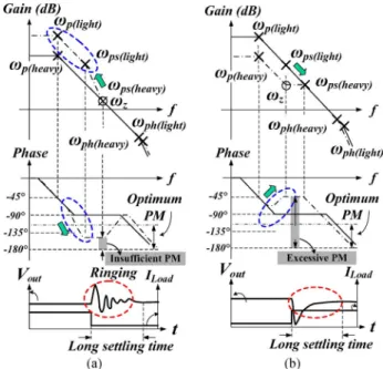
As shown in Fig. 4(a), is designed to cancel at heavy loads. When load current changes from heavy to light, moves toward the origin due to its characteristic of load depen-dence. The PM would deteriorate since the compensation zero cannot be moved back to cancel the system pole at light loads. It might suffer the ringing problem and the long settling time resulting from the insufficient PM in transient period. More-over, when is designed to cancel the system pole at light loads as depicted in Fig. 4(b), the PM becomes larger than the optimal value. It has opposite performance to the requirement of fast transient response at heavy loads. The system is always stable but carries out the slow transient response because of the large PM.
Therefore, an adaptive compensation zero is needed in the current-mode buck converter to ensure large system bandwidth and adequate PM at any load conditions. The compensation zero should be located at low frequencies to cancel the effect of the system pole at light loads and be moved toward high frequencies
(1) (2) where
Fig. 3. (a) Compensation network in the design of the voltage-mode DC-DC buck converter. (b) Frequency response.
to cancel the effect of the system pole at heavy loads. During the load transient period, the dip output voltage depends on the ESR value of output capacitor and the system bandwidth. However, the voltage drop across the ESR is a material-related value. To maintain a large system bandwidth and adequate PM is therefore an effective way to enhance the power management module. Therefore, the proposed fast transient with APM control tech-nique can achieve the fast and smooth load transient response through the control of compensation pole-zero pair.
III. PROPOSEDFASTTRANSIENTCONTROLPROCEDURE
WITHAPM
The control-to-output transfer function of the conventional current mode DC-DC buck converter has two separated real poles, and , [19], [20]. is located at the output of the regulator, that is, where is the output filter capacitor and load resistance is inversely proportional to load current . The output pole is therefore propor-tional to the value of load current . Besides, the high-fre-quency pole is located near the switching frequency region because of the characteristic of the current programmed control.
Fig. 4. Different positions of in steady state. (a) designed at high fre-quencies to cancel at heavy loads, causes the PM worse at light loads. (b) designed at low frequencies to cancel at light loads, causes the PM larger than the optimum PM.
It pushes the inductor-resulted pole to a high-frequency posi-tion to separate the double pole at output stage. The compen-sation method only needs to increase the low-frequency loop gain using the PI compensation to improve transient regulation performance.
The transfer function of an equivalent PI compensation tech-nique proposed by [2] is given as (4). and are expressed in (5), where and are on-chip small compensation re-sistor and capacitor, respectively. is the output resistance of the error amplifier (EA) and its value is much larger than that of . is the transconductance of the OTA [21]. is the capacitor multiplier factor
(4) (5) A low-frequency pole-zero pair, and , can effectively com-pensate the current-mode DC-DC buck converter. This is be-cause that the current generated by EA can be redirected to charge or discharge the small on-chip capacitor in compensation network for on-chip compensation. Moreover, the fast transient mechanism can be simultaneously achieved in case of load cur-rent variation [22].
Fig. 5 shows the proposed structure of the fast transient con-trol with the APM technique in a current-mode buck converter. An adaptive compensation resistance can achieve the APM technique to get the adequate system phase margin under dif-ferent load conditions. In addition, an adaptive compensation capacitance is implemented to further achieve fast and smooth transient response. As the fast transient technique in [2], the one-shot control is used to decide the duration of the fast transient period. However, it suffers from an oscillation problem when the positive feedback gain is larger than one.
Fig. 5. Proposed compensation circuit is composed of the adaptive capacitance and resistance in current-mode buck converter.
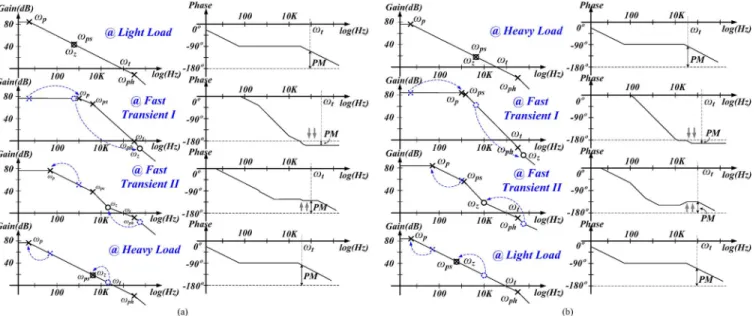
Fig. 6. Frequency response of the proposed current-mode buck converter at different loads. (a) The positions of , , and when load current changes from light to heavy. (b) The positions of , , and when load current changes from heavy to light.
Thus, the proposed adaptive compensation technique contains four steps to complete the fast transient response. The frequency response expression of the fast transient with APM control is shown in Fig. 6. At first, the system is in steady-state and waits for the occurrence of load transient response. When load current changes from light to heavy as depicted in Fig. 6(a), and are moved toward high frequencies to improve the tran-sient response because of the small equivalent compensation capacitance and large system bandwidth. It is different from the technique proposed in [2] since is controlled by output voltage and current at the same time. is at lower frequencies than that of in the previous design [2] to derive a large system bandwidth. After the fast transient I (FTI) period, and start to move back to the position in steady state when the transient procedure enters the fast transient II (FTII) to alleviate the oscillation problem. At this time, and still position at high frequencies to get a fast recovery time. Finally,
and are moved back to the position in steady state.
Owing to the adaptive with the ability to adjust the resis-tance in the PI compensator, the position of is no longer sim-ilar to that in [2] because it reaches the position of at heavy loads to achieve nearly exact pole-zero cancellation. Due to the pole-zero cancellation generated by the proposed adaptive compensation capacitance and resistance circuit, not only the system bandwidth can be magnified but also PM can be main-tained a suitable value, which is near 60 degrees, to wait for load variations in steady state. On the other hand, is located at high frequencies at heavy loads. Therefore, when load current changes from heavy to light as illustrated in Fig. 6(b), and are moved toward to high frequencies during the FTI. After FTI, and start to move back toward the origin during the FTII. Finally, at the end of transient response, is located at a low frequency position, which is close to the system pole at light loads, to achieve nearly exact pole-zero cancellation. Ob-viously, the proposed fast transient control with an APM can improve the transient response time during the transient period.
Besides, PM in steady state can be improved due to the nearly exact pole-zero cancellation. PM can be kept a suitable value to ensure the system stability at any loads.
Moreover, the performance of load transient response in the current-mode buck converter is determined by the output impedance and the loop crossover frequency. The load transient response of power management module can be evaluated by the transient dip voltage and the settling time, which can be indicated by the closed-loop output impedance. The accurate model of the current programmed control buck converter has been presented in [23]. The open-loop output impedance
can be shown as (6)
where
(6) is the switching cycle of the buck converter. is the com-pensation slope. is the complement of duty cycle
. Besides, based on the proposed structure depicted in Fig. 5, the transfer functions of EA, the adaptive compensation resistance circuit, the adaptive compensation capacitance cir-cuit, and the control to output voltage gain can be merged as a factor shown in (7). represents the transfer function of the power stage in current-mode buck converter. In addition, the voltage divider at the output node of buck converter is con-sidered as the feedback factor expressed in (8). Therefore, the closed-loop output impedance can be shown in (9)
(7) (8)
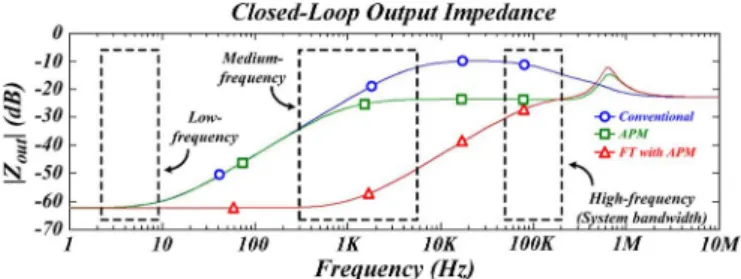
(9) Fig. 7 shows the output impedance of the current mode buck converter with conventional method, the APM technique, and the proposed FT control with the APM technique. The load transient response can be explained by the closed-loop output impedance in three different frequency regions. The closed-loop output impedance in high-frequency region can indicate voltage drop in the beginning of transient response. That is, the initial dip voltage in load transient response is the consequence of the closed-loop output impedance derived near the loop crossover frequency. As shown in Fig. 7 in high-frequency region, the closed-loop output impedance of both the APM technique and the FT control with APM technique are almost equivalent with a smaller value than that of the conventional method. Smaller closed-loop output impedance at the loop crossover frequency would come to a smaller transient dip voltage. Consequently, the transient voltage drop of the proposed FT control with the APM technique can be smaller than that of the conventional
Fig. 7. Closed-loop output impedance of the buck converter with different con-trol techniques.
method owing to the smaller closed-loop output impedance at the loop crossover frequency. The closed-loop output impedance in the high-frequency region near the crossover frequency is shown in (10) simplified from (9), which is proportional to the ratio between the output resistance of EA and the compensation resistance
at high frequencies
(10)
In medium-frequency region of the closed-loop output impedance shown in Fig. 7, the proposed FT control with the APM technique also derives the smallest output impedance compared to those of the conventional method and the tech-nique with APM only. The settling time in load transient response is also affected by the closed-loop output impedance within the loop crossover frequency. Smaller closed-loop output impedance would achieve shorter transient settling time. Therefore, the proposed FT control with the APM technique can derive the shortest settling time compared to the other control methods.
Moreover, the closed-loop output impedance in the medium-frequency region can be simplified as (11) from (9).
is influenced by , , and
at medium frequnecies
(11) In the low-frequency region, the value of the output impedance is equivalent to the others. It indicates that the proposed technique would not affect the steady-state error. As a result, the proposed FT control with the APM technique can adjust the adaptive compensation capacitance and resistance to get smaller closed-loop output impedance, which carries out smaller transient dip voltage and transient settling time in the current-mode buck converter.
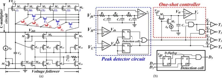
Fig. 8. Implementation of the adaptive compensation circuit. (a) The schematic of the adaptive compensation capacitance. (b) One-shot controller decides the first fast-transient period and the peak detector decides the second fast-transient period.
IV. CIRCUITIMPLEMENTATIONS
A. Adaptive Compensation Capacitance
The adaptive capacitance circuit can automatically adjust the value of compensation capacitance by controlling the current flowing through the small capacitor as shown in Fig. 8(a). As a result, the capacitor can be amplified to an optimum value for system compensation in steady-state or adjusted to a small value in load transient period to accelerate the system response [22], [24]–[26].
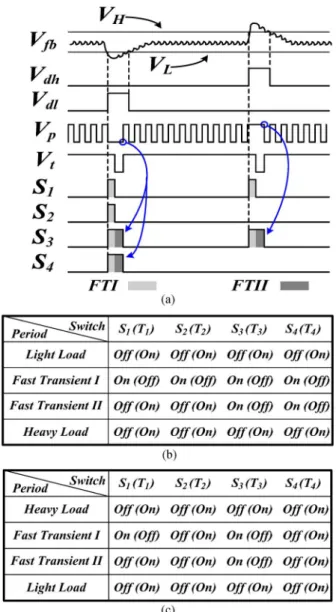
The operation of the adaptive capacitance circuit is separated into four steps. Step 1 is in steady-state. Switches are opened ( are closed) so that the current flowing through transistors can not flow into the small on-chip ca-pacitor . It acts as a current source parallel with the current flowing through to achieve the on-chip compensation [2]. The function of the adaptive capacitance circuit in this step is to maintain a large on-chip compensation capacitance. Besides, peak detector circuit and one-shot controller shown in Fig. 8(b) are used to control the fast transient operation. The low-pass filter in the peak detector circuit can react the feedback voltage variation to the oscillating signal , which is utilized to de-termine the duration of fast transient response according to dif-ferent load current steps. The larger load step will lead to the longer transient period. Thus, when the feedback voltage is larger than the high threshold voltage or smaller than the low threshold voltage , the fast transient mechanism would be activated. The fast transient period contains two steps, which are step 2 named as FTI and step 3 named as FTII.
In step 2 (or FTI), or in the peak detector circuit are set to high to trigger the detection cell, which is composed of two D-flip-flops, to enable the one-shot controller. The control time diagram of the adaptive compensation capacitance circuit is shown in Fig. 9(a). The switches are closed and are opened when the load current changes from light to heavy ( , , , and are closed but , , , and are opened when the load changes from heavy to light). That is, a large current would directly inject into the small on-chip capacitor at this period. Thus, the equivalent capacitance
value of the adaptive capacitance is decreased in order to accelerate the transient response.
At the end of the one-shot period, is set to high and the fast transient response enters step 3 (or FTII). Switches and are opened but and are still closed ( and are closed; and are opened) when the load current changes from light to heavy ( , , , and are closed but , , , and are opened when the load changes from heavy to light). The current flowing into the small on-chip capacitor is less than that in step 2. Hence, the equivalent value of the adaptive capacitance becomes larger than that in step 2, so that the compensation zero is pulled toward the origin to increase the PM and stabilize the system.
Finally, would send an edge trigger to the detection cell to end the fast transient operation. The positive or negative trigger of is generated when output voltage is returned back from the undershoot or overshoot, respectively. The period of the fast transient control, which is determined by the low-pass filter in the peak detector circuit, is proportional to the output load transient condition. When the operation enters into step 4 of steady-state, switches are opened ( are closed) and the adaptive capacitance is again amplified to a large ca-pacitance. Accompanied with an adaptive resistance , which has a small value at heavy loads or a large value at light loads, the nearly exact pole-zero cancellation is achieved in order to extend the system bandwidth and PM. The states of these eight switches in fast transient period are shown in Fig. 9(b) and (c). Two-stage fast transient operation in step 2 and step 3 has these advantages. 1) The system can be stabilized since the PM in step 3 is better than that in step 2 owing to the larger compen-sation capacitance. 2) The output voltage can be smoothly regulated back to its steady-state value with little overshoot and undershoot because of the smooth control of compensation pole-zero pair. 3) The low-pass filter in peak detector circuit achieves the load-dependent control of adaptive capacitance circuit that would dynamically determine the fast transient pe-riod according to different load current condition. Moreover, the predefined voltage and in the peak detector circuit of Fig. 8(b) is derived from the bandgap reference.
Fig. 9. Control scheme of the adaptive compensation circuit. (a) Time di-agram of the one-shot controller and peak detector circuit. (b) The status of the eight switches when load current changes from light to heavy. (c) The status of the eight switches when load current changes from heavy to light.
Due to the implementation of auxiliary switches as depicted in Fig. 8(a), the value of on-chip compensation capacitance can be adjusted in the FT period. It can be considered that the transconductance of EA would be varied at the different periods of the FT response since the value of compensation capacitance, which is changed with a constant-biasing EA, is derived in the FT period. As shown in Fig. 10(a), the transcon-ductance of EA with an auxiliary gain stage for the on-chip capacitor is increased from to , , and , respectively. The is the steady-state transcon-ductance of EA. Once the system enters into fast transient of
step 2, the value of the equivalent transconductance becomes
and since the load changes from heavy to light or from light to heavy, which is expressed as (12). Similarly, the equivalent transconductance of the step 3 is derived as (13). When load current changes from heavy to light, the multiplier
factors and define the amplified
factors in FTI and FTII, respectively. On other hand, when
Fig. 10. (a) Transconductance of the transconductance amplifier with an aux-iliary gain stage for the on-chip capacitor . (b) The schematic of EA.
TABLE I
TRANSCONDUCTANCECOEFFICIENTS OFEA WITH ANAUXILIARYGAINSTAGE
load current changes from light to heavy, the multiplier factors and define the amplified factors in FTI and FTII, respectively. is the entire capacitance multiplier factor in the adaptive compensation capacitance circuit. The schematic of the EA in the proposed structure is depicted in Fig. 10(b). The coefficients in (12) and (13) are listed in Table I
(12) (13)
Fig. 11. Current sensing circuit with the SH circuit.
In order to prevent the converter from oscillating and en-sure the system stability, a conservative value of the time du-ration is used to design first step pulse in FTI period to de-crease output overshoot/undershoot. Since the APM technique, the adaptive resistance at light loads is larger than that at heavy loads. Hence, the adaptive capacitance should be de-creased to a smaller value when the load changes from light to heavy than that when the load changes from heavy to light. Therefore, and should be larger than and
, respectively.
B. Current Sensing With Sample-and-Hold Circuit
According to the theorem of current mode control, the system pole at output node is inversely proportional to load resis-tance. In other words, the position of is proportional to the load current. The current sensing circuit with a sample-and-hold (SH) circuit [27] as depicted in Fig. 11 is used to derive the value of load current, and thereby moving the position of the compensation zero to the position where locates. When the signal changes from high to low, the power p-MOSFET is turned on to deliver energy from power source to the in-ductor and the output. Simultaneously, the transistor is also turned on to connect the drain of to the non-inverting input of the op-amp. Thus, the transistors and can sense the current flowing through the power p-MOSFET . The current flows through is used to generate the sensing voltage for the operation of current-mode DC-DC buck converter. On other hand, the current that flows thorough is mirrored by the cur-rent mirror pair and to generate a current to the SH circuit. When the signal of is triggered from high to low, the sensing current is averaged by the SH circuit and thus the value of average inductor current can be derived by the signal .
Furthermore, in order to alleviate the effects of clock shoot-through and charge injection, a complement transistor is connected as a dummy switch and controlled by the signal . Owing to the current sensing circuit, the value of the sensing current, which is scaled down to times that of load current, is sampled and averaged by the SH circuit. After the I-V conversion across the resistor , the averaged inductor current value is converted to as shown in (14)
where is a constant (14)
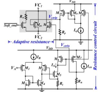
Fig. 12. Adaptive resistance control circuit.
C. Adaptive Compensation Resistance
The position of the compensation zero is inversely propor-tional to the product of the compensation resistance and capac-itance. To get an adequate PM at any load condition, needs to be adjusted adaptively to track the output load condition. As illustrated in Fig. 12, an adaptive resistance control circuit is used to derive the load-dependent compensation zero for the cancellation of the output pole . The control signal gen-erated from the current sensing with a SH circuit indicates the averaged inductor current and can be used to control the posi-tion of to achieve a nearly exact pole-zero cancellation at different load condition. However, this adaptive resistance con-trol circuit would not work properly with the uncertainty load condition during the start-up period. Thus, a small resistor is designed to place parallel with the transistors and to eliminate this scenario.
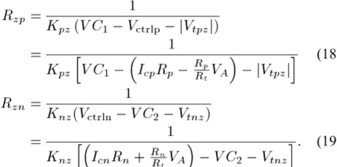
When the start-up period ends, the signal will be set to low to disconnect the current flowing through the resistor . The parallel MOSFETs and are operated in deep triode region as the equivalent resistances and , which have their values determined by the gate controlling signals and . These gate controlling signals are generated by the resistance control circuit in Fig. 12. in (14) indicates the load condition, and thereby being used to adjust the posi-tion of . is converted to a current as expressed in (15) through the voltage-to-current (V-I) structure and utilized in the determination of and in (16) and (17). Two constant currents, and , are generated to ensure the deep triode op-eration of the MOSFETs and . Therefore, the equiv-alent resistances and can be determined in (18) and (19), respectively
(15) (16) (17)
(18)
(19) and are the threshold voltages and and are the products of the mobility and aspect ratio of the transistors
and , respectively. An equivalent resistance , which determines the position of , is equal to the value of . Assuming that and have the similar value in steady-state operation, the inverse value of the equivalent resistance in (20) is proportional to the load condition to achieve the compensation zero adjustment. Hence, the exact expression of the compensation zero can be derived in (21). The effects of the output pole on the PM can be effectively alleviated due to the tracking of the compensation zero
where and (20) where and (21) Fig. 13 is the simulation result of the adaptive circuit. The gate control signals, and , would be modulated according to the load-dependent signal . The resistance would be inverse proportional to the load current to achieve the adaptive compensation. Table II lists the locations of the dom-inant pole , the output pole and the compensation zero during the load transient period between 100 and 500 mA. These movements are achieved through the proposed adaptive compensation technique. Moreover, to implement the transis-tors and in parallel can deal with the sudden load variations. When load current changes from light to heavy rapidly, the output node of error amplifier can be raised to a higher voltage level immediately. It results in a large voltage difference between nodes and , and thereby pushing the transistor into the saturation region. The equivalent
re-Fig. 13. Simulation of the adaptive compensation resistance circuit.
TABLE II
LOCATIONLIST OFALLPOLES ANDZERO
sistance across transistor would become very large. Fortu-nately, the transistor still operate in deep triode region as a linear resistance that the compensation zero can be held prop-erly in order to prevent the oscillation problem. Similarly, the transistor may operate in the saturation region at the be-ginning of transient response due to the instant decrease at node . However, transistor can still work in the deep triode region to form an adaptive compensation resistance for the adaptive compensation. It is obvious that the fast transient con-trol and the nearly exact pole-zero cancellation are achieved.
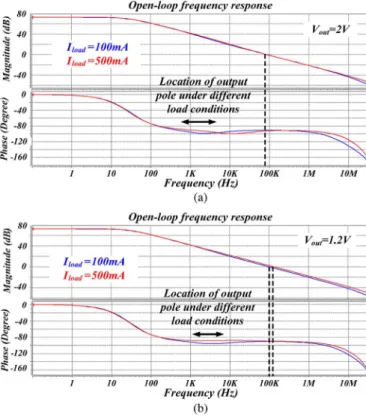
In the proposed structure with the FT technique and the APM method, the variation of compensation resistance is in the range from 150 to 800 k when the load changes from heavy load to light load. The variation of is in the range of 2 to 200 pF in load transient period owing to the adaptive compen-sation capacitance circuit. Fast transient period is determined by the value of load current steps to ensure the smooth tran-sient response and to prevent the overcharge and undercharge issues. Moreover, the APM method with the adaptive compen-sation resistance circuit adjusts the compencompen-sation resistance for deriving the optimal compensation zero. These mechanisms can guarantee both and to be adjusted in the designed range. The simulated results of the open-loop frequency response of the proposed buck converter at both different output voltages and different load conditions are shown in Fig. 14.
V. EXPERIMENTALRESULTS
The proposed technique was fabricated with 0.35 m CMOS process. The chip micrograph and the PCB layout are shown
Fig. 14. Simulated results of open-loop frequency response of the proposed buck converter at different load conditions. (a) 2 V. (b) 1.2 V.
in Fig. 15(a) and Fig. (b), respectively. The total silicon area is about 2000 m 1900 m, including the testing pads. The silicon overhead of the FT control with APM technique is only 150 m 140 m. The external inductor and capacitor are 4.7 H and 10 F, respectively. The switching frequency is 1 MHz. The output voltage ripple is about 15 mV. Fig. 15(c) shows the photo of the wireless USB receiver.
Fig. 16 shows and inductor current when steps from 100 to 500 mA, or vice versa. The overshoot and under-shoot voltages are 38 and 60 mV, respectively. The transient recovery times of undershoot and overshoot voltages are 6 and 12 s, respectively. It is obvious that the performance of the proposed technique has small overshoot/undershoot voltage and setting time when load current suddenly changes. The wave-form demonstrates that the adaptive and can increase the system bandwidth and PM according the instant load current condition.
Fig. 17 shows the comparison between the proposed FT con-trol with the APM technique, the conventional design without any fast transient techniques, and the design with APM tech-nique only. As shown in Fig. 16, when steps from 100 to 500 mA, the undershoot voltages of three results are 60 mV for the proposed method, 84 mV for the method with APM only, and 110 mV for the conventional design. The proposed method has the best performance due to the FT control with APM technique during load transient period. Besides, owing to the APM technique, the adaptive resistance is adjusted according to the load condition. Thus, when the load suddenly changes from light load to heavy load, the adaptive resistance would be set as a larger value than that in conventional method since the adaptive system compensation is achieved at
Fig. 15. (a) Chip micrograph. (b) PCB layout. (c) Wireless USB receiver.
Fig. 16. Waveforms of the load transient response.
light load. Therefore, the smaller closed-loop output impedance can be derived near the loop crossover frequency compared to conventional method through (10). The transient dip voltage is about 85 mV in conventional design and 60 mV achieved by the APM technique.
Besides, the transient recovery times are 6 s for the pro-posed method, 45 s for the method with only APM, and 42 s for the conventional design. The closed-loop output impedance below the loop crossover frequency can affect the transient set-tling time. The closed-loop output impedance at the medium-frequency region shown in (11) is influenced by the system com-pensation coefficient. The proposed FT control with the APM technique can dynamically adjust the compensation capacitance and resistance during the load transient response. That is, when
Fig. 17. Measured load transient response when load changes from 100 to 500 mA with the three fast transient techniques by separating three output waveforms.
Fig. 18. Measured load transient response when load changes from 500 to 100 mA with the three fast transient techniques by separating three output waveforms.
TABLE III
RELATIVECOEFFICIENTS OFOUTPUTIMPEDANCE
the load transient occurs, the FT control can minimize the com-pensation capacitance. Thus, the closed-loop output impedance can be derived as a smaller value due to the proposed FT control with the APM technique, which achieves the shortest voltage re-covery time.
Fig. 18 shows the transient recovery time and the overshoot voltage between the three results when changes from 500 to 100 mA. Certainly, the performance of the proposed method is better than those of two results. The overshoot voltages of three results are 38 mV for the proposed method, 58 mV for the method with only APM, and 60 mV for the conventional
TABLE IV
COMPARISON OF THERELATEDFASTTRANSIENTMETHOD
Fig. 19. Comparison in current consumption under different fast transient tech-niques in the design of current-mode DC-DC converters.
TABLE V
SPECIFICATIONS OF THEPROPOSEDCONVERTER
design. Moreover, the transient recovery times are 12 s for the proposed method, 62 s for the method with only APM, and 58
s for the conventional design.
Table III shows the relative coefficients for the output impedance in the proposed buck converter of the FT control with APM technique. Owing to the adaptive compensation, the closed-loop output impedance can be varied when the fast transient mechanism is activated.
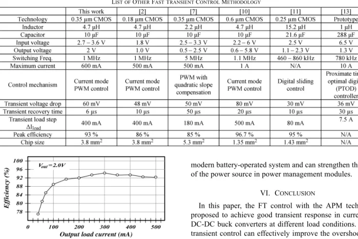
Table IV lists the comparison with the related method of fast transient techniques in the design of DC-DC converters. Obvi-ously, the proposed FT control with the APM technique has the better performance than those of other fast transient techniques.
Fig. 20. Power conversion efficiency of the proposed converter.
Fig. 19 shows the current consumption of four different design methods. Owing to the small overhead of the implemen-tation in the adaptive resistance, the current consumption of the APM technique is increased about 20 A compared to the conventional design. Besides, the current consumption of the positive feedback is larger than that of the conventional about 100 A. Thus, the FT control with APM technique needs more 70 A quiescent current than that of the conventional design. Moreover, the APZP technique reported in [2] can has the good transient response but lead to a large current consumption owing to the combination of adaptive frequency control (AFC) technique.
Fig. 20 shows the power conversion efficiency of the pro-posed DC-DC converter through the FT control with APM tech-nique. The efficiency can be kept at 92% at medium to heavy loads. The light-load efficiency is deteriorated to 78% at load current 40 mA. The reason is that the operation of the con-verter enters the discontinuous conduction mode (DCM) opera-tion and thus the switching loss dominates the total power con-sumption. Therefore, the operation can be switched to dithering skip-modulation (DSM) or pulse frequency modulation (PFM) operation [28] to improve the power conversion efficiency. The detail specifications of the proposed DC-DC buck converter are listed in Table V.
Table VI shows the list of other popular fast transient control methodologies. The fast transient response and the small output voltage ripple are the advantages of the proposed converter. The proposed FT control with the APM technique is suitable to the
modern battery-operated system and can strengthen the quality of the power source in power management modules.
VI. CONCLUSION
In this paper, the FT control with the APM technique is proposed to achieve good transient response in current-mode DC-DC buck converters at different load conditions. The fast transient control can effectively improve the overshoot/under-shoot voltage and the transient recovery time. The compen-sation pole-zero pair can be dynamically moved toward high frequencies during transient period. After the output voltage is regulated to its steady-state value, the compensation pole-zero pair is smoothly moved back to the steady-state position. Thus, the overshoot/undershoot voltage can be decreased. Besides, owing to the APM technique, the compensation zero is moved to nearly close to the position of the system pole to achieve the pole-zero cancellation. Thus, the PM of the system can be always kept an adequate value in steady state. Experimental results show that the overshoot/undershoot voltage is smaller than 60 mV and the transient response time is smaller than 12 s as load current suddenly changes from 100 to 500 mA, or vice versa. Compared with conventional designs without any fast transient technique, the performances of undershoot voltage and recovery time are enhanced by 45% and 85%, respectively.
ACKNOWLEDGMENT
The authors would like to thank Energy Pass Incorporation for their help.
REFERENCES
[1] G. Patounakis, Y. W. Li, and K. L. Shepard, “A fully integrated on-chip DC-DC conversion and power management system,” IEEE J.
Solid-State Circuits, vol. 39, no. 3, pp. 443–451, Mar. 2004.
[2] C.-Y. Hsieh and K.-H. Chen, “Adaptive pole-zero position (APZP) technique of regulated power supply for improving SNR,” IEEE Trans.
Power Electron., vol. 23, no. 6, pp. 2949–2963, Nov. 2008.
[3] H.-W. Huang, H.-H. Ho, C.-C. Chien, K.-H. Chen, G.-K. Ma, and S.-Y. Kuo, “Fast transient DC-DC converter with on-chip compensated error amplifier,” in Proc. Euro. Solid-State Circuits Conf., 2006, pp. 324–327.
[4] H.-W. Huang, K.-H. Chen, and S.-Y. Kuo, “Adaptive frequency controltechnique for enhancing transient performance of DC-DC con-verters,” in Proc. Euro. Solid-State Circuits Conf., 2007, pp. 174–177. [5] L. Chen and B. Ferrario, “Adaptive Frequency Compensation for
DC-to-DC Converter,” U.S. Patent 20 060 176 098, Aug. 10, 2006. [6] C.-H. Tso and J.-C. Wu, “A ripple control buck regulator with fixed
output frequency,” IEEE Power Electron. Lett., vol. 1, pp. 61–63, Sep. 2003.
[7] K. Umimura, H. Sakurai, and Y. Sugimoto, “A CMOS current-mode DC-DC converter with input and output voltage-independent stability and frequency characteristics utilizing a quadratic slope compensation scheme,” in Proc. Euro. Solid-State Circuits Conf., 2007, pp. 178–181. [8] A. Barrado, A. Lázaro, R. Vázquez, V. Salas, and E. Olías, “The fast response double buck DC-DC converter (FRDB) operation and output filter influence,” IEEE Trans. Power Electron., vol. 20, no. 6, pp. 1261–1270, Nov. 2005.
[9] J. J. Chen, F. C. Yang, and C. C. Chen, “A new monolithic fast-response buck converter using spike-reduction current-sensing circuits,” IEEE
Trans. Ind. Electron., vol. 55, no. 3, pp. 1101–1111, Mar. 2008.
[10] F.-F. Ma, W.-Z. Chen, and J.-C. Wu, “A monolithic current-mode buck converter with advanced control and protection circuit,” IEEE Trans.
Power Electron., vol. 22, no. 5, pp. 1836–1846, Sep. 2007.
[11] J. Kim and M. A. Horowitz, “An efficient digital sliding controller for adaptive power-supply regulation,” IEEE J. Solid-State Circuits, vol. 37, no. 5, pp. 639–647, May 2002.
[12] J. Xu, G. Zhou, and M. He, “Improved digital peak voltage predictive control for switching DC-DC converters,” IEEE Trans. Ind. Electron., vol. 56, no. 8, pp. 3222–3229, Aug. 2009.
[13] V. Yousefzadeh, A. Babazadeh, B. Ramachandran, E. Alarcón, L. Pao, and D. Maksimović, “Proximate time-optimal digital control for syn-chronous buck DC-DC converters,” IEEE Trans. Power Electron., vol. 23, no. 4, pp. 2018–2026, Jul. 2008.
[14] K. K.-S. Leung and H. S.-h. Chung, “A comparative study of the boundary control of buck converters using first- and second-order switching surfaces,” IEEE Trans. Power Electron., vol. 22, no. 4, pp. 1196–1209, Jul. 2007.
[15] W.-T. Yan, C. N.-M. Ho, H. S.-H. Chung, and K. T. K. Au, “Fixed-fre-quency boundary control of buck converters with second-order switching surface,” IEEE Trans. Power Electron., vol. 24, no. 9, pp. 2193–2201, Sep. 2009.
[16] M. Karppanen, J. Arminen, T. Suntio, K. Savela, and J. Simola, “Dy-namical modeling and characteristics of peak-current-controlled su-perbuck converter,” IEEE Trans. Power Electron., vol. 23, no. 3, pp. 1370–1380, May 2008.
[17] E. Figueres, G. Garcera, J. M. Benavent, M. Pascual, and J. A. Mar-tinez, “Adaptive two-loop voltage-mode control of DC-DC switching converters,” IEEE Trans. Ind. Electron., vol. 53, no. 1, pp. 239–253, Feb. 2006.
[18] Y. S. Lai and C. A. Yeh, “Predictive digital-controlled converter with peak current-mode control and leading-edge modulation,” IEEE Trans.
Ind. Electron., vol. 56, no. 6, pp. 1854–1863, Jun. 2009.
[19] R. W. Erickson and D. Maksimović, Fundamentals of Power
Elec-tronics. Norwell, MA: Kluwer, 2001.
[20] C. M. Lia, S. J. Chiang, C. Y. Lai, K. H. Pan, G. C. Pan, and G. S. Hsu, “Modeling and controller design of a current-mode controlled converter,” IEEE Trans. Ind. Electron., vol. 41, no. 2, pp. 231–240, Apr. 1994.
[21] J. Roh, “High-performance error amplifier for fast transient DC-DC converters,” IEEE Trans. Circuits Syst. II, Exp. Briefs, vol. 52, no. 9, pp. 591–595, Sep. 2005.
[22] K.-H. Chen, C.-J. Chang, and T.-H. Liu, “Bidirectional current-mode capacitor multipliers for on-chip compensation,” IEEE Trans. Power
Electron., vol. 23, no. 1, pp. 180–188, Jan. 2008.
[23] B. B. Ridley, “A new, continuous-time model for current-mode con-trol,” IEEE Trans. Power Electron., vol. 6, no. 2, pp. 271–280, Apr. 1991.
[24] G. A. Rincon-Mora, “Active capacitor multiplier in miller-compen-sated circuits,” IEEE J. Solid-State Circuits, vol. 35, no. 1, pp. 26–32, Jan. 2000.
[25] I.-C. Hwang, “Area-efficient and self-biased capacitor multiplier for on-chip loop filter,” IEEE Electron. Lett., vol. 42, no. 24, pp. 1392–1393, Nov. 2006.
[26] G. Palumbo and S. Pennisi, “A high-performance CMOS voltage fol-lower,” in Proc. IEEE Int. Conf. Electron. Circuits Syst., 1998, vol. 2, pp. 21–24.
[27] B. Razavi, Design of Analog CMOS Integrated Circuit. New York: McGraw-Hill Higher Education, 2001.
[28] H.-W. Huang, K.-H. Chen, and S.-Y. Kuo, “Dithering skip modulation, width and dead time controllers in highly efficient DC-DC converters for system-on-chip applications,” IEEE J. Solid-State Circuits, vol. 42, no. 11, pp. 2451–2465, Nov. 2007.
Yu-Huei Lee (S’09) was born in Taipei, Taiwan. He received the B.S. and M.S. degrees from the Department of Electrical and Control Engineering, National Chiao Tung University, Hsinchu, Taiwan, in 2007 and 2009, respectively. He is currently pursuing the Ph.D. degree in the Institute of Elec-trical Control Engineering, National Chiao Tung University, Hsinchu, Taiwan.
He is a faculty member with the Mixed-Signal and Power Management IC Laboratory, Institute of Elec-trical Control Engineering, National Chiao Tung Uni-versity, Hsinchu, Taiwan. His current research interests include the power man-agement integrated circuit design, LED driver IC design, and analog integrated circuits.
Shao-Chang Huang received the B.S. and M.S. degrees in electrical engineering from the National Cheng Kung University, Tainan, Taiwan, in 1994 and 1996, respectively, and the Ph.D. degrees from the Department of Electrical and Control Engineering, National Chiao Tung University, Hsinchu, Taiwan, in 2011.
From 1996 to 1998, he was an Officer in National Compulsory Military Service. From 1998 to 1999, he was engaged in thin-film-transistor device at ERSO, ITRI, Taiwan. From 1999 to 2006, he worked on ESD/Latch-up/IO research in UMC, Ltd., HBA, Ltd., TSMC, Ltd. and NO-VATEK, Ltd. As a UMC engineer, he worked on 90 nm process ESD solutions at IBM, Fishkill, NY, in 2001. Since the end of 2006, he joined eMemory Technology, Taiwan, where he is currently the ESD/IO Department Manager. He is the author or coauthor of more than 8 papers published in journals and conferences, and he holds more than 20 patents. His current research interests include ESD/Latch-up devices and circuits, and I/O related circuits.
Shih-Wei Wang was born in Hualien, Taiwan, in 1980. He received the B.S. degree from the Department of Electrical Engineering, National Taiwan University of Science and Technology, Taipei, Taiwan, in 2006, and the M.S. degree from the Department of Electrical and Control Engi-neering, National Chiao Tung University, Hsinchu, Taiwan, in 2010, where he is currently pursuing the Ph.D. degree in the Institute of Electrical Control Engineering.
His research interests include the design of switch-mode power converters, linear regulators, analog integrated circuits, and mixed-signal integrated circuits.
Ke-Horng Chen (M’04–SM’09) received the B.S., M.S., and Ph.D. degrees in electrical engineering from National Taiwan University, Taipei, Taiwan, in 1994, 1996, and 2003, respectively.
From 1996 to 1998, he was a part-time IC De-signer with Philips, Taipei, Taiwan. From 1998 to 2000, he was an Application Engineer with Avanti, Ltd., Taiwan. From 2000 to 2003, he was a Project Manager with ACARD, Ltd., where he was engaged in designing power management ICs. He is currently an Associate Professor with the Department of Electrical Engineering, National Chiao Tung University, Hsinchu, Taiwan, where he organized a Mixed-Signal and Power Management IC Laboratory. He is the author or coauthor of more than 80 papers published in journals and conferences, and also holds several patents. His current research interests include power management ICs, mixed-signal circuit designs, display algo-rithm and driver designs of liquid crystal display (LCD) TV, red, green, and blue (RGB) color sequential backlight designs for optically compensated bend (OCB) panels, and low-voltage circuit designs.