ELECTROCHEMICAL SOCIETY LETTERS
Electrical Characteristics and Annealing Study of
Boron-Doped Polycrystalline Diamond Films
Sheng-Hsiung Chen," Shen-Li Chenf Ming-Hsing Tsaifl J. J. Shyufl and Chia-Fu Chen a
alnstitute of Materials Science and Engineering, National Chiao Tung University, Hsinchu 30050, Taiwan bDepartment of Electrical Engineering, Da-Yeh Institute of Technology, Chang-Hwa 515, Taiwan
ABSTRACT
Annealing processes are an important area of fundamental research within the field of diamond electronic applications. In this study, annealing was applied to as-grown boron-doped diamond films. The current-voltage (I-V) characteristics of the AI/boron-doped diamond films were also investigated. First, the conductivity of films was examined to determine the effect of annealing on boron-doped diamond films. Experimental results indicated that the activation energy for the as-deposited diamond films (intrinsic or light boron-doped ) is about 0.38 eV. After annealing, the activation energy did not change. However, the activation energy of the heavily doped films remarkably would change to 0.014 eV after annealing. Next, Fourier transform infrared spectroscopy (FTIR) and cathodoluminescence (CL) were performed to understand more clearly the correlation between the activation energy and the annealing effect on B-doped diamond films. These results revealed that for the lightly B-doped films, the boron atoms were effectively activated at the substitutional site. For the heavily doped case, boron was initially located in an inactive site (e.g., grain boundary, interstitial or clustering sites) and would diffuse into the substitutional site after 900~ annealing.
Diamond films, which are wide bandgap and have the highest thermal conductivity, are highly suitable for high-temperature elec- tric device applications. Detailed information concerning the elec- tronic and optical properties of CVD diamond films must be collected and analyzed. Some improvements in the electronic prop- erties of CVD diamond films have recently been made, 1-5 and the activation energy was used to examine the improvement of electri- cal properties. Masood et al. 6 reported Hall and resistivity meas- urements on lightly B-doped polycrystalline diamond films with ac- tivation energies of 0.38 eV. They concluded that the small Hall mobility can be traced back to the influence of grain boundaries. On the other hand, for heavily B-doped diamond film studies, Nishimura 5 and his co-workers considered the small activation en- ergies in terms of impurity band conduction and suggested that the influence of grain boundaries and sp 2 components on the transport properties is small. In this paper, the study of the annealing process provides relevant information regarding the diffusion of impurity centers in diamond films. Results obtained in this study indicate that annealing on the sample of heavily doped diamond films en- hances the electrical properties of boron-doped diamond films.
The samples used in this work were fabricated by standard mi- crowave-plasma enhanced chemical vapor deposition processes. N-type Si (100) substrates were scratched using diamond powder (approximately 1 - 2 #m) to enhance the nucleation density of deposits. Next, the scratched Si substrates were dipped into a solution of HF: HaO = 1 : 100 for a few seconds to remove the native oxide on the silicon. A vapor source of trimethylborate [B(OCHa)3] was introduced to the CH4-CO2 gas mixtures. The flow rate of trimethylborate varied from 0 (0%) to 5 sccm ( 8% B/C ratio in the gas phase) using a mass flowmeter.
The as-deposited diamond films were annealed in a helium ambi- ent atmosphere at temperatures of 400, 700, and 900~ respec- tively, for 30 min. In order to remove the nondiamond surface layer, the diamond films were cleaned by dipping them in a mixture of HF + HNO3 + H20 and then in a saturated solution of CrO3 in H2SO4 at 145~ for 20 min. This procedure was followed by rinsing in a 1:1 boiling solution of H202 and NHaOH. Aluminum contacts (-5000 A) were formed by lift-off procedure. The activation energy was calculated from the Arrhenius plot (p vs. temperature) from the I-V measurement. Fourier transform infrared spectroscopy (FTIR), and cathodoluminescence (CL) experiments were used to examine the effects of annealing on the boron-doped diamond. For the measurement of CL spectra, the electron beam voltage was 15 kV, the beam current was 70 I~A, and the spot size on the specimen was estimated to be 0.5 t~m. Infrared data were taken with a reso-
lution of 2 cm 1 over the range 3200-500 cm -1. Infrared spectra recorded by using pellets of freestanding diamond films com- pressed with KBr provided better resolution of the boron-doped diamond films than the conventional methods. I-V measurements of the two configurations [Le., two pads on the same surface method and back bias (sandwich) method] were taken to examine whether interference would occur with conductivity by interface. Therefore, the former method is used in this work.
The temperature dependence of the conductivity was measured with a constantly applied voltage. The full lines correspond to the theoretically calculated curves. 7 From these curves, the activation energies of the current were eva_luated and shown in Fig. 1, which were 0.38, 0.34, 0.32, and 0.31 eV for boron-doped films deposited
~ ,
10 -3
"7E~
l0 g
e) "7..~ 10 4
O. ~ 10 -6
1 0 -7 , , , i , , , , i , , , ~ i J ~ , , i , ,( d ) ,
Q~O
-(C) %'0 *
"0. ( b ) ~ . ~
"~e~o. o Ea=0.31 eV
" ~ n ~
Ea=0"32 eV
Ea=0.34 eV
Ea=0.38 eV
10 ~
, . . I . , , , , . . . , I . . . ., , ,
2.0
2.5
3.0
3.5
4.0
1000/T (K q)
Fig. 1. Conductivity as a function of temperature for various concentrations of boron-doped diamond films with (a) B(OCH3)3 = 0 sccm; (b) B(OCH3)3 = 0.01 sccm; (c) B(OCH3)3 = 2 sccm; and (d) B(OCH3)3 = 5 sccm. The flow ratio of COz/CH4 was 30 (sccm)/21 (sccm), 30 (sccm)/20.4 (sccm), 30 (sccm)/ 19 (sccm), and 30 (sccmy18.4 (sccm).
J. Electrochem. Soc., Vol. 142, No. 12, December 1995 9 The Electrochemical Society, Inc. L223
) unless CC License in place (see abstract).
ecsdl.org/site/terms_use
address. Redistribution subject to ECS terms of use (see
140.113.38.11
L224 J. Electrochem. Soc., Vol. 142, No. 12, December 1995 9 The Electrochemical Society, Inc.
"7
0"7,
10 ~
l0 -1
.. 10 -2
9
.~,~ l0 -3
9
.~ 10 -4
0
10-5
' ' ' I . . . . ! . . . . I . . . . I ' '(c)
Ea=O.O14 e ~
Co)
" ( a ) ~ ~ _ ~ n E a = 0 . 3 1
eV"
Ea=0.31 eV"
. , , , I , . . . I . . . . I . . . . I . .2.0
2.5
3.0
3.5
4.0
1000/T
(K -1)
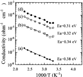
Fig. 2. Conductivity as a function of temperature for boron- doped diamond films with [CH4]/[CO~] = 18.4 (sccm)/30 (sccm) and B(OCHs)3 = 5 sccm, using annealing temperatures of (a) 400, (b) 700, and (c) 900~
with the flow rate of trimethylborate set at 0, 0.01, 2, and 5 sccm, respectively. In these depositions, the flow rate of CH4 was reduced to adjust the carbon concentration, which increased with the addi- tion of trimethylborate. The values of conductivity are in agreement with earlier reportfl It can be seen that the bulk conductivity follows the Arrhenius law and the activation energy is almost the same as that of type lib diamond (0.37 eV). ~ However, the higher doping concentration would imply the lower the activation energy, Le., sim- ilar to the behavior reported for diborane-doped films. 1~ This phe- nomenon can be accounted for as follows: the high doping concen- tration produces a band in the acceptor level, thereby causing a reduction in the the energy difference between the acceptor level and the top of the valence band. Moreover, earlier measurements of E~ for CVD diamond films showed values in the range 0.26- 0.38 eV which are consistent with E~ value of Fig. 1. Moreover, as indicated in Fig. 1, a lightly doped [B(OCHa)s = 0.01 sccm, trimethylborate diluted by methanol] sample was examined, and the conductNity was found-to have increased slightly. This increase would imply that light doping is effective. Furthermore, the conduc- tivity of the B-doped diamond films as a function of inverse temper- ature can be seen in Fig. 1. For synthetic B-doped diamonds it has been shown" that conductivity at low temperatures can be ex- pressed in terms of variable-range hopping, Le., conductivity de- creased with decreasing temperature, which are attributed to conduction through variable-range hopping between acceptor cen- ters produced by substitutional atoms] ~ It has been observed for heavily doped, ~2 synthetic, lz~3 and chemical vapor deposition diamond. T M
Annealing treatment on nondoped and lightly doped diamond films showed no obvious difference as compared with those of as-deposited films. The conductance did not change, and the acti- vation energy exhibited no obvious change. However, the heavily doped films showed a different trend. Figure 2 indicates that three different temperatures were used in annealing the heavily doped samples [B(OCH3)3 = 5 sccm]. This figure also revealed that the activation energy remained at about 0.31 eV when annealing temperatures of 400 and 700~ were used. After annealing at 900~ however, the activation energy of the heavily doped films remarkably changed, dropping to 0.014 eV. CVD diamond films were grown on substrates at around 800~ and the higher temper- ature annealing will result (900~ in a significant change in activa- tion energy. Discovering the actual reason for this change was the ultimate objective of this work. However, the much lower activation energy indicated that annealing at 900~ would significantly alter the electrical properties of the heavily doped samples.
Although some authors have studied the electrical properties of boron-doped diamond films, no report has been published regard-
ing infrared (IR) properties of B-doped diamond films focusing on annealing study. Mort et al. 15 described the IR characteristics of diamond films using B2H6 as a boron source. In this study, the IR absorption characteristics of doped diamond films were also measured using heavily doped conditions [B(OCHs)s = 5 sccm]. Annealing was carried out for a period of 30 min at 400, 700, and 900~ An IR absorption spectrum ranging from 3200 to 500 cm 4 is shown in Fig. 3. These results indicate that, for diamond films, an sp 3 C-H stretching absorption peak appears in the range 2855- 2950 cm-1; however, the appearance of a C-H bond can be at- tributed to the large number of nonequilibrium hydrogen atoms present in the plasma when the diamond films were deposited. The C-H bond absorption peak significantly decreases as the annealing temperatures increase.
Boron-doped diamond films have absorption peaks appearing at 2461,2800, and 2929 cm 1 , which are induced by a transition from ground to the first, second, and third excited state, respectively] 6'~7 In Fig. 3a and b, the absorption peaks of the excited states of boron atoms are not obvious. However, they are quite clear in Fig. 3c, suggesting that doping of the heavily doped samples would be more effective and hold three boron excited states after 900~ annealing. A sharp absorption peak appearing at 1440 cm 4 and a small peak at around 1280 cm 4 can be attributed to the bonding effect of C-B] 8 The intensity of the two peaks clearly increased as the annealing temperature increased. As is generally known, if the boron was incorporated and located at the substitutional sites in the diamond films, the carbon and boron would have a covalent bond (C-B bonding) between these two kinds of atoms. At the same time, the C-B bonding would not be created if the boron is located at interstitial or clustering sites. Since the C-H content in the heavily doped .films reduces after annealing and C-B bond intensity increased, we suspect-that the conductivity increase is primarily a result of the boron having effectively diffused into the substitutional site after 900~ annealing. From above results, the C-H content in the lightly or heavily doped films reduced after annealing, and was commonly ascribed to an increase in the bulk resistivity due to a dehydrogenation of the diamond films] 9 However, a decrease in resistivity was detected, thereby leading us to the conclusion that the H atom functions in an impurity role that causes the conductivity to not be as significant as the boron atom.
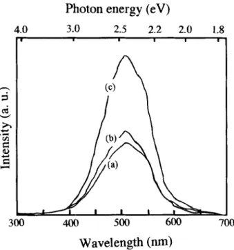
Cathodoluminescence (CL) is one of the most useful techniques for studying wide-bandgap semiconductor materials such as a diamond. Here, cathodoluminescence spectroscopy (Fig. 4) was used to examine the differences for the same samples correspond- ing to Fig. 2. Accordi.ng to Ruan et aL, 2~ there are two dominant peaks for diamond films, the broad luminescence bands centered around 2.83 and 2.32 eV in undoped and relatively heavily doped samples, respectively. They conclude that the 2.32 eV peak is due to boron-related centers and the 2.83 eV band is due to dislocations in diamond. In our work, only the peak at 2.32 eV was found, presumably due to the samples being heavily doped diamond films. This can be clearly seen from Fig. 4. The annealing temperature increases from curve "a" to curve "c" as we mentioned above. What we can see in this figure is that with the increase of annealing temperature, the intensity of the peak at around 2.32 eV increases. Particularly, the peak dramatically increased after 900~ annealing.
g
O<
~
"
Oco)
x••(a)
| ! ! a |3000
2500
2000
1500
1000
500
Wavenumber (cm-')
Fig. 3. Fourier transform infrared spectroscopy (FTIR) measured from the same samples shown in Fig. 2.
) unless CC License in place (see abstract).
ecsdl.org/site/terms_use
address. Redistribution subject to ECS terms of use (see
140.113.38.11
J. Electrochem. Soc., Vol. 142, No. 12, December 1995 9 The Electrochemical Society, Inc. L225
o~
300
Photon energy (eV)
4.0
3.0
2.5
2.2
2.0
1.8
|
|
I
i
i
| 7(a/~f//)
" ~ ~
| I I
400
500
Wavelength (nm)
| ~ _ .
__
600
700
Fig. 4. CL spectra measurement for the same samples shown in Fig. 2.
From the change in the intensity of CL at 2.32 eV, the amount of substitutional boron in the boron-doped diamond films apparently increased by the annealing treatment. The above data suggest that more substitutional boron atoms were obtained because of anneal- ing. Furthermore, annealing alters the activation energy of the boron-doped diamond films.
In summary, the activation energy of the as-deposited intrinsic or lightly doped diamond films was about 0.38 eV. After 900~ anneal- ing, although the C-H content decreased, theoretically, the conduc- tivity of diamond films must be decreased by several orders of magnitude. However, not only was the conductivity increasing but also the activation energy of the heavily doped films would drop remarkably to 0.014 eV. Furthermore, annealing would improve the electrical properties of boron-doped diamond films. In conjunction with the results on the electrical conductivity and its temperature dependence by means of the Fourier transform infrared spec- troscopy and cathodluminescence measurements confirmed that boron doping from a gas phase precursor is substitutional in nature for a lightly doped case. tn another case, boron appears on inactive sites during heavy doping. Furthermore, annealing initially causes
boron atoms in inactive sites (e.g., interstitial or clustering sites) to
be incorporated into substitutional sites. The electrical properties were also altered.
Acknowledgments
The authors would like to thank the National Science Council of the R.O.C. for financial support of this manuscript under Contract No. NSC 84-2221-E009-036.
Manuscript submitted Feb. 17, 1995; revised manuscript re- ceived Sept. 6, 1995.
National Chiao Tung University assisted in meeting the publica- tion costs of this article.
REFERENCES
1. K. Miyata and D. L. Dreifus, Jpn. J. AppL Phys., 33, 4526 (1994).
2. I.M. Buckley Golder and A. T. Collins, Diamond and ReL Mat.
1, 1083 (1992).
3. M. Werner, O. Dorsch, H. U. Baerwind, and E. Obermeier,
Appl. Phys. Lett., 64, 595 (1994).
4. M. Werner, O. Dorsch, H.-U. Baerwind, E. Obermeier, C. Johnston, P. R. Chalker, and S. Romani, IEEE Trans. Electron Devices., ED-42, 1344 (1995).
5. K. Nishimura, K. Das, and J. T. Glass, J. AppL Phys., 69, 3142 (1991).
6. A. Masood, M. Aslam, M. A. Tamor, and T. J. Potter, Appl. Phys. Lett., 61, 1832 (1992).
7. K. Okano, H. Naruki, Y. Akiba, T. Kurosu, M. lida, T. Hirose, and T. Nakamura, Jpn. J. Appl. Phys., 28, 1066 (1989). 8. J.L. Daison, R. Ramesham, and C. Ellis, This Journal, 137,
3206 (1990).
9. J.E. Field, Properties of Diamond, p. 99, Academic Press, London (1973).
10. Y. Sato, M. Kamo, and N. Setaka, in High Tech Ceramics, P.
Vincenzini, Editor, p. 1719, Elsevier, Amsterdam (1987). 11. A. W. S. Williams, E. C. Lightowlers, and A. T. Coltin,
J. Phys. C. 3, 1727 (1978).
12. A.T. Collins and A. W. S. Willians, J. Phys. C, 4, 1789 (1971). 13. J. C. Bourgoin, J. Krynicki, and B. Blanchard, Phys. Status
SolidiA, 52, 293 (1979).
14. N. Setaka, Paper presented at MRS Spring '89 Meeting, San Diego, CA 1989 (unpublished).
15. J. Mort, M. A. Machonkin, and K. Okumura, Appl. Phys. Lett.,
48, 1908 (1991).
16. S.D. Smith and W. Talor, Proc. Phys. Soc., 79, 1142 (1962). 17. F. Zhang, E. X. B. Ang, Y. Cai, and G. Chen, Mater. Lett., 19,
115 (1994).
18. The Infrared and Electro-Optical System Handbook: V.7, Countermeasures, S. R. Robinson, Editor, p. 353 (1993). 19. M. I. Landstrass and K. V. Ravi, Appl. Phys. Lett., 55, 97
(1990).
20. J. Ruan, K. Kobashi, and W. J. Choyke, ibid., 60, 3138 (1992).
) unless CC License in place (see abstract).
ecsdl.org/site/terms_use
address. Redistribution subject to ECS terms of use (see
140.113.38.11
![Fig. 2. Conductivity as a function of temperature for boron- doped diamond films with [CH4]/[CO~] = 18.4 (sccm)/30 (sccm) and B(OCHs)3 = 5 sccm, using annealing temperatures of (a) 400, (b) 700, and (c) 900~](https://thumb-ap.123doks.com/thumbv2/9libinfo/7606148.129574/2.864.76.416.63.435/conductivity-function-temperature-boron-diamond-ochs-annealing-temperatures.webp)