An Efficient VLSI Architecture for Full-Search Block Matching Algorithms
CHEN-YI LEE AND MEI-CHENG LU
Dept. of Electronics Eng. & Institute of Electronics, National Chiao Tung University, Hsinchu, Taiwan Received July 8, 1994; Revised March 29, 1996; Accepted April 25, 1996
Abstract. This paper presents a novel memory-based VLSI architecture for full search block matching algo-rithms. We propose a semi-systolic array to meet the requirements of high computational complexity, where data communications are handled in two styles: (1) global connections for search data and (2) local connections for partial sum. Data flow is handled by a multiple-port memory bank so that all processor elements function on target data items. Thus hardware efficiency achieved can be up to 100%. Both semi-systolic array structure and related memory management strategies for full-search block matching algorithms are highlighted and discussed in detail in the paper.
1. Introduction
Video codecs for video phone and video conference systems have become available as a result of recent progress in video coding techniques [1, 2]. Among them, motion estimation is one of the key components of high-compression video codecs. The most popular technique for motion estimation is the block matching algorithm (BMA) for a simple hardware implementa-tion. However, the computational complexity inherent in BMA lies in the following factors: (a) frame rate, (b) frame size, and (c) search area. Figure 1 shows that for a typical BMA, a current frame is divided into a block of pixels (N× N) which are often named refer-ence data. The block of pixels is compared with the corresponding candidate blocks within a search area of size(N + 2P) × (N + 2P) in the previous frame. Here P is the maximum displacement allowed in both horizontal and vertical directions. Motion vector is ob-tained from the displacement whose distortion is the minimum among all candidates within the search area. For MPEG2 main profile at main level [3], frame rate and frame size are 30 and 720× 480 respectively. The displacement(P) ranges from 4 to 1024. However for
∗Work supported by the National Science Council of Taiwan, ROC, under Grant NSC84-2213-E009-115.
practical applications, P is often limited to 16. Thus, there are 30× 720 × 480 × (2 × 16 + 1)2/N2 candi-date blocks should be processed within 1 second. For each candidate, there are N× N pixels to be processed and each pixel requires 3 operations (subtract, abso-lute, and accumulate [4]), then at least 33.8 GOPs are needed for N= 16. This is obviously out of the range which current general-purpose or domain-specific pro-cessors can handle. Therefore parallel processing tech-niques are highly demanded for real-time performance in this case.
Many architectural solutions for implementing BMA can be found in the literature [4–9]. Most of the solutions concentrated on the data flow within pro-cessor element (PE) array. Therefore systolic array approach has been highly exploited in VLSI imple-mentation. However, this approach causes some prob-lem in data flow outside PE array. In other words, too much overhead on memory bandwidth is requested to provide a scheduled data sequence in order to meet the need of PE array. Therefore large number of I/O pins is needed, resulting in higher packaging cost. In addition, due to pipeline filling at the boundary of search area and long latency in data initialization, hardware efficiency becomes degraded a lot. Although, in [8, 9], the au-thors proposed a snake-like data stream format which can reduce the I/O bandwidth problem, the hardware
P1: ICA/SFI P2: SSK/TKL QC: MVG
Journal of VLSI Signal Processing Kl417-06-Lee March 10, 1997 11:54
276 Lee and Lu
Figure 1. Illustration of the motion estimation process between reference block(N × N) and candidate blocks (2P + 1)2on search area.
efficiency still remains very low. Moreover, up to now, very few papers discuss the issue of reducing long la-tency in data initialization. On the other hand, most papers assume that both reference data and search area are available whenever needed. In practical applica-tions, this is not true because those data are either from imaging source or from buffer memory. For 2-D ar-ray implementation of ME processor, many data have to be initialized before all PEs work on correct data items.
In this paper, we propose a semi-systolic array to improve the low efficiency problem as found in sys-tolic array solutions. Instead of local connections of search data flow, we use a global distribution of search data connected to each PE row (or column). The par-tial sum is locally connected. With this style, it has been proved that hardware efficiency up to 100% can be achieved if a dedicated memory management unit is supported. Section 2 describes how the general BMA algorithms can be mapped onto the proposed semi-systolic array or SSA architecture. The data flow within PE array will also be highlighted. Section 3 presents the memory management strategy in order to offer the scheduled data sequence as well as to cope with long latency in data initialization so that 100% efficiency can be achieved in PE array. Then a demonstrator de-sign of motion estimation processor for N= P = 16 is described in Section 4, where much emphasis will be on the design of PE and controller structure. Finally we have some evaluation data and discussions on the proposed memory-based SSA architecture style.
2. Mapping BMA onto Semi-Systolic
Array Architecture
Systolic array (SA) [10] is a good solution for pro-cessing large volumes of multi-dimensional data. It is
Figure 2. Illustration of the semi-systolic array architecture.
also suitable for VLSI implementation due to locality, regularity, and modularity [10, 11]. A systematic ap-proach for mapping algorithms onto SA structure can be found in [11]. However, as mentioned in the previ-ous section, the problem of the SA architecture lies in low hardware efficiency due to pipeline filling and data initialization. In this section, we first propose a semi-systolic array (SSA) architecture and then describe how BMA can be mapped onto the SSA architecture.
2.1. The SSA Architecture
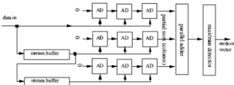
The basic structure of the SSA is shown in Fig. 2. In this structure, the connections are divided into two types— one is broadcasting or global distribution type and the other is local type. For broadcasting type, input data is fed in from the stream memory and connected to all PEs of the same row (column). For local type, results obtained from the left (bottom) PEs are pumped into next right (upper) PEs for further processing. It can be seen that the main difference between SA and SSA is the broadcasting of input data. In fact, this broadcasting signal is avoided in SA due to violation of locality. However, we can exploit this broadcasting feature to improve the hardware efficiency as described below.
2.2. Mapping Full Search Motion Estimation Algorithm onto SSA
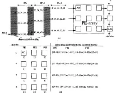
To illustrate how full search motion estimation opera-tions can be mapped onto the SSA architecture, we use an example of a 3× 3 reference block with search area of 7× 7 as shown in Fig. 3. In this example, N and P are 3 and 2 respectively. Furthermore, we assume that the distortion of each candidate block can be par-titioned into row (or column) based summation as the following equations: MAD(u, v) = N X i=1 PSiuv (1)
Figure 3. An example for demonstrating the efficiency of SSA with
N= 3 and P = 2.
Figure 4. Example of a BMA realized on the SSA structure, with
N= 3 and P = 2. However, hardware efficiency becomes degraded
due to boundary situation where search data have to be filled in the PE array. where PSiuv= N X j=1 ADuv(i, j) (2)
ADuv(i, j) = |S(i + u, j + v) − R(i, j)| (3) and−P ≤ u, v ≤ P.
The ADuv(i, j) represents the absolute difference of search data (S) and reference data (R). The PSiuv repre-sents the partial sum of the absolute differences for the i th row. Equation (2) implies that the computation of PSkuvand PSluv, for l6= k, are mutually independent and can be performed simultaneously. Therefore the full-search block matching can be operated in a parallel way. First we assume that reference data have been stored in each PE, then search data are pumped out from the stream memory and broadcast to PEs which perform absolute mean calculation and partial sum accumula-tion as shown in Fig. 4. With the latency of 6 cycles, the first distortion comes out from the bottom right cell (ACC). Then the distortion values of the rest candidates are obtained sequentially. However, when boundary is detected, some PEs become idle since data of the next row (column) have to be filled to the pipeline. There-fore, the efficiency obtained from Fig. 4 is about 50% for N = P = 8, which is similar to the approach used in [8].
Figure 5. (a) Improve hardware efficiency using multiple inputs so that search data can be filled in the PE array and (b) shows an example how hardware efficiency can be improved by parallel ports when boundary is detected.
This low efficiency can be overcome by preloading data of next row before boundary is detected. As shown in Fig. 5(a), when the distortion calculation is done on the boundary candidate, data of the next row should be pumped into PE array at the next cycle. The mask region indicates that these data should be simultane-ously pumped into the PE-array. Figure 5(b) illustrates the process of distortion calculation at boundary. At cycle 5, boundary is detected. Summation of the dis-tortion values of different candidates are still performed at PE1, j, j = 1, 2, 3. At cycle 6, the boundary block
still needs the boundary data (label 16) which should be pumped into PE2 and PE3. However, data of the next row (i.e., label 21) should be pumped into PE1. At cycle 7, data items (labels 17 and 22) are needed. Distortion calculation of the candidate on the boundary is achieved now in PE3. In the meantime, distortion of the candidates of the next row are also performed in PE2 and PE1. At cycle 8, only the data items from the same row are needed. Therefore the BMA can be mapped onto the semi-systolic array, where no idle op-erations are identified in the PE-array.
3. Memory Management
In the previous section, we showed that hardware ef-ficiency obtained from the SSA architecture can reach 100% if the desired data flow can be scheduled in ad-vance. This section describes the design of a data-flow arrangement unit to conduct this specific task.
P1: ICA/SFI P2: SSK/TKL QC: MVG
Journal of VLSI Signal Processing Kl417-06-Lee March 10, 1997 11:54
278 Lee and Lu
Figure 6. Search data is organized in a snake stream format to meet scheduled data flow within PE-array.
When candidate blocks are not within the boundary area, only one single data stream is needed for all PEs on the same row. However when boundary candidate is detected, two data streams are needed. This implies that a two-read-port memory is needed. In addition, the data items fetched from the current stream memory have to be loaded into next stream memory. This snake-like data stream format is shown in Fig. 6. Therefore a two-write-port memory is also needed. As a result from these read/write considerations, it is necessary to provide a 2-port memory with size of(N −1)×(2P+1) for non-boundary data and a 4-port memory with size of(N − 1) × (N − 1) for boundary data. However, since storage space is only activated once at a certain time interval, the 4-port memory devices can be re-duced to 2-port memory with the constraint that these
(N − 1) × (N − 1) boundary data should use different
read/write ports.
We still have to consider the problem of data initial-ization since this problem may cause idle operations within the PE array. In the previous discussion, we first assumed that reference data (N × N) and part of search data (N − 1) × (2P + N) are preloaded into PE array and stream memory banks respectively. However, at(2P + 1)2cycle, distortion calculation for the last candidate block will be finished except the la-tency inherent in pipeline delay. If we have to fill in the stream memory banks, then all PEs are idle for at least
(N − 1) ∗ (2P + N) cycles. Therefore we propose
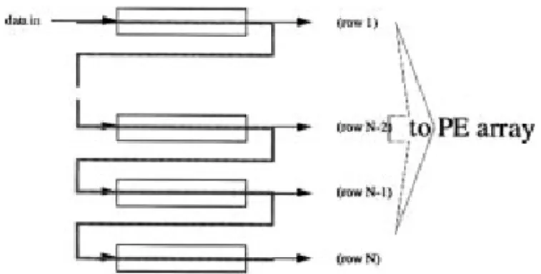
to use interleaving stream memory banks, i.e., there are two identical stream memory bank units which are working on different search area as shown in Fig. 7. While stream memory bank 1 (SMB1) is for current search area data, SMB2 can be used to preload part of the search data, i.e.,(N −1)×(2P+N), for calculating next motion vector. Thus once distortion calculation for the last candidate block of current candidate block is done, we can immediately switch from SMB1 to SMB2
Figure 7. Organization of the stream memory banks. Note that these two identical banks are working interleavely to reach 100% efficiency.
Figure 8. The shift register array is allocated on the other side of PE array for two purposes: Delay matching and preloading reference data. (a) Shows delay matching of partial sum and (b) preloading ref-erence data for next motion vector calculation through interleaving.
for calculating next motion vector if next reference data are already available. To ensure that reference data are already available, we need one N × N shift register array (SRA). However, this SRA is also needed for matching partial sum sequence to get final distortion value as shown in Fig. 8(a). Since one SRA cannot be shared for delay management and storing reference data, we use two SRA’s which are interleaved as shown in Fig. 8(b).
Based on this organization, the total memory space needed is 2(N − 1) × (N + 2P) + 2(N × N), where the former part is for search data and the latter part is for both delay management and reference data. To minimize the number of data communication ports, we
are selected. In this case, K should be at least 3, and the total memory space becomes 1952.
4. VLSI Architectures
for Real-Time Performance
In this section, we discuss a real-time motion estima-tion processor design based on the proposed SSA ar-chitecture mentioned earlier, where N = P = 16 are selected. The design can be directly used in MPEG2 at Main profile at Main level where BMA motion es-timation can be handled by one single chip. The ME processor is partitioned into 5 units as shown in Fig. 9. Since stream memory banks (SMB), processor element array (PEA), and shift register array (SRA) are the spe-cific features of this chip, they will be discussed in more detail below.
4.1. Architecture for PE Array
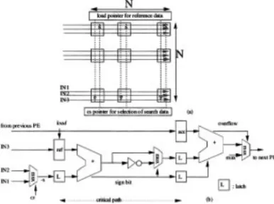
The PE-array is organized as shown in Fig. 10(a), where 3 global data buses are over PEs on the same row. Basically, the required operations within each PE are: subtract, absolute, and add. However we have replaced the subtract by another add operation in order to mini-mize the area of each PE. That is we take the inverted signal of the search data when they are pumped into the PE array. Note that these operations are pipelined into two stages—the first stage is for add and absolute. The search data are first latched and then its absolute value is latched at the second pipe. The second stage is for add operation together with an overflow detector to limit the distortion value as shown in Fig. 10(b). The three global data buses are connected to IN1, IN2, and IN3.
Figure 9. Block diagram of the motion estimation processor with
N= P = 16.
Figure 10. (a) Structure within the PE array and (b) the detailed design of each PE which contains two pipeline stages.
In the initial phase, reference data are loaded into the ref register which is done simultaneously with the search data. After the first N cycles, these reference data are stored in the PE array. Then these reference data can be used for the rest candidate blocks. The loading process of these reference data are controlled by the load pointer which is above the PE array. For the cs pointer, which is used to select the data stream of search area, is controlled by the read pointer needed in stream memory banks. Both load and cs pointers can be realized by shift registers (or ring-counter structure) which are also used in the SRA for delay matching and preloading reference data.
4.2. Stream Memory Banks
This unit is designed to provide the scheduled data flow which is needed by the PE array. The overall structure is given in Fig. 11, where two stream memory banks are in the center and 2 read/write pointers are located at the top and bottom positions. The read and write pointers are working simultaneously except that these two pointers have different phases. Note that the first 2P+ 1 memory elements use one read/write port and the rest N − 1 elements use another read/write port. Therefore we have to provide special read/write point-ers which are discussed below.
Since only one of the two read ports is accessed at a certain time, we can merge these two pointers into one single pointer. For example, when the boundary can-didate is detected, the read pointer provides two read signals used to simultaneously access two search data items which are also loaded into next stream memory.
P1: ICA/SFI P2: SSK/TKL QC: MVG
Journal of VLSI Signal Processing Kl417-06-Lee March 10, 1997 11:54
280 Lee and Lu
Figure 11. The architecture for the stream memory banks, which consists of 2× (N − 1) × (2P + N) 2-port memory in the center and 2 sets of read/write pointers on the top and bottom.
In this way, the basic cell can be reduced to two-port memory cell. The operations of read/write pointers are summarized as follows: the read pointer is first acti-vated to read search data out from the stream memory. The search data is then connected to PE array, and in the meantime, they are also stored in next stream memory. In addition, this read pointer is also connected to the cs pointer used in PE array for stream data selection. To speed up the design cycle for this dedicated memory, a memory generator has been developed [12]. It can automatically generate the memory size according to the given parameters, such as N and P.
4.3. Shift Register Array Unit
This unit is designed to handle reference data as well as delay matching for the partial sum of distortion. In gen-eral, when this SRA unit is served for delay matching, only(N −1)× N/2 storage space is needed. However, in physical layout design, it is not regular. In addition, we also consider the use of buffer for reference data. Therefore the storage space of N× N is selected (see Fig. 8). Here two SRA units are working in an in-terleaving way. While one of the SRA’s is for delay matching, the other is for preloading reference data of next motion vector.
For delay management, the top row has the min-imum delay of 1 cycle while the bottom row has the maximal delay of 16 cycles. In this way, partial sums produced in each PE row are accumulated at the correct sequence. In other words, distortion value
corresponding to one candidate block becomes avail-able at the bottom accumulator after(2N + 2) cycles. Also it takes 16× 16 cycles to load reference data into the SRA unit. However this process can be simultane-ously done during the calculation of motion vectors.
5. Evaluation and Discussions
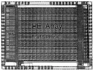
Based on the proposed architecture, a proto-typing ME processor has been designed and fabricated. Results show that its clock rate up to 100 MHz can be achieved, implying that about 97,600 MV’s can be obtained ev-ery second. Area for the proto-typing ME processor is about 9.5 × 7.2 mm2based on 0.8µm CMOS double metal technology [13]. Figure 12 shows the final lay-out. Characteristics of the ME chip are summarized as follows:
• transistor-count: 310 K
• internal buffer size: 1,952 × 8 bits • clock rate: 100 MHz (max.) • die size: 9.5 × 7.2 mm2
• I/O packaging: 84-pin PGA
• technology: 0.8 µm CMOS SPDM process • performance: 48,800 MV @ 50 MHz (for MPEG2
MP @ ML)
• power consumption: 1.95 W @ 5 V, 50 MHz • search range: [−16, +15]
It can be found that our proposed architecture can produce one MV every 1024 cycles, which is the op-timum for 1024 candidates. The memory size used in our proposal is about 4 times of [8], however, the
Figure 12. Chip plot of the SSA-based motion estimation processor design with N= P = 16.
performance. Our proposal can handle this problem be-cause of the double buffering scheme.
In summary, the SSA-based ME processor has the following features:
• optimal usage of PE array: each PE’s efficiency can
reach 100%;
• simple control flow: the required control signals for
each module are rather simple and can easily be de-rived from ring-counter logic;
• selection of different displacements (P): this can
be done by adjusting the read/write pointers at the stream memory banks, where the cycle count for calculating each motion vector is(2P)2 for search
range of [−P, P − 1].
• selection of different sizes of reference block: this
can be done by adjusting the position of the input port of the stream memory banks.
• minimum I/O bandwidth: both reference and search
data are accessed once and buffered internally for re-quired operations; for neighbouring reference block, part of search area can be directed obtained from in-ternal buffer due to double buffering scheme. In this way, I/O bandwdith can further be reduced.
6. Conclusion
In this paper, we have presented a novel VLSI architec-ture for optimally implementing full-search motion es-timation algorithm. The proposed architecture mainly consists of (1) PE-array which is a semi-systolic array structure to offer computation power and (2) stream memory bank which offers a scheduled search data flow so that 100% hardware efficiency within the PE-array can be achieved. In addition, this proposed architecture is also flexible in selecting the sizes of reference and search blocks. The architecture has also been demon-strated by an ME processor which generates one mo-tion vector every(2P)2 cycles. Test results from the
demo chip also show the feasibility of ME processor for digital video based on current VLSI technology. We are currently investigating the possibility of scalable solution for large search area based on this proposed architecture.
References
1. R. Srinvasan and K.R. Rao, “Motion-compensated coder for video conferencing,” IEEE Trans. on Communications, Vol. COM-35, pp. 297–304, March 1987.
2. Y. Ninomiyya and Y. Ohtsuka, “A motion compensated inter-frame scheme for television pictures,” IEEE Trans. on
Commu-nications, Vol. COM-30, pp. 201–211, Jan. 1982.
3. “International Organization for Standardization Coding of Mov-ing Pictures and Associated Audio,” ISO/IEC JTC1/SC29 WG11/602, Seoul, Nov. 1993
4. K. Komarek and P. Pirsch, “Array architectures for block match-ing algorithms,” IEEE Trans. on Circuits and Systems, Vol. 36, No. 10, pp. 1301–1308, Oct. 1989.
5. R.C. Kim and S.U. Lee, “A VLSI architecture for a pel recur-sive motion estimation algorithm,” IEEE Trans. on Circuits and
Systems, Vol. 36, No. 10, pp. 1291–1300, Oct. 1989.
6. L. De Vos and M. Stegherr, “Parameterizable VLSI architectures for the full-search block matching algorithm,” IEEE Trans. on
Circuits and Systems, Vol. 36, No. 10, pp. 1309–1316, Oct. 1989.
7. K.M. Yang, M.T. Sun, and L. Wu, “A family of VLSI designs for the motion compensated block-matching algorithm,” IEEE
Trans. on Circuits and Systems, Vol. 36, No. 10, pp. 1317–1325,
Oct. 1989.
8. C.H. Hsieh and T.P. Lin, “VLSI architecture for block-matching motion estimation algorithm,” IEEE Trans. on Circuits and
Sys-tems for Video Technology, Vol. 2, No. 2, pp. 169–175, June
1992.
9. S.I. Uramoto, A. Takabatake, M. Suzuki, H. Sakurai, and M. Yoshimoto, “A half-pel precision motion estimation processor for NTSC-resolution video,” in IEEE Custom Integrated Circuits
Conference, San Diego, CA, May 9–12, 1993, pp. 11.2.1–11.2.4.
10. H. T. Kung, “Why systolic architectures,” IEEE Computer, Vol. 15, No. 1, Jan. 1982.
11. S.Y. Kung, VLSI Array Processors, Prentice-Hall International Editions, 1988.
12. G.L. Tzeng and C.Y. Lee, “An efficient memory architecture for motion estimation processor design,” in Proc. of ISCAS’95, April 29–May 3, 1995.
13. M.C. Lu and C.Y. Lee, “Semi-systolic array based motion esti-mation processor design,” in Proc. of ICASSP’95, Detroit, May 8–12, 1995.
14. J. Baek, S. Nam, M. Lee, C. Oh, and K. Hwang, “A fast array ar-chitecture for block matching algorithm,” in Proc. of ISCAS’94, London, May 30–June 2, 1994, pp. 4.211–4.214.
15. C.L. Wang, K.M. Chen, and J.M. Hsiung, “A high-throughput and flexible VLSI architecture for motion estimation,” in Proc.
of ICASSP’95, Detroit, May 8–12, 1995, pp. 3295–3298.
16. H. Yeo and Y.H. Hu, “A novel modular systolic array architecture for full-search block matching motion estimation,” IEEE Trans.
on CAS for Video Technology, Vol. 5, No. 5, pp. 407–416, Oct.
P1: ICA/SFI P2: SSK/TKL QC: MVG
Journal of VLSI Signal Processing Kl417-06-Lee March 10, 1997 11:54
282 Lee and Lu
Chen-Yi Lee received B.S. from National Chiao Tung University,
Taiwan in 1982, M.S. and Ph.D. from Katholieke University Leuven (KUL), Belgium in 1986 and 1990 respectivley, all in Electrical En-gineering. From 1986 to 1990, he was with IMEC/VSDM, working in the area of architecure synthesis for DSP. Since Feb. 1991, he has been an associate professor in the Dept. of Electronics Engineering at the National Chiao Tung University, Hsinchu, Taiwan.
His research interests mainly include video/image coding, high-speed networking, digital communications, VLSI architectures, and system-level synthesis.
Mei-Cheng Lu received the B.S. and M.S. degrees in Electronics
Engineering from National Chiao Tung University in June 1993 and 1994 respectively. Since Aug. 1994, she has been with the Sili-con Integrated Systems Corp., Hsin-Chu, Taiwan, as a design engi-neer working in the area of chip-set solutions for high-performance PC.
Her research interests mainly include VLSI architecture, data com-pression, and architecture performance analysis.