Characterization of 380 nm UV-LEDs grown on free-standing GaN by
atmospheric-pressure metal-organic chemical vapor deposition
C. Y. Shieh
1, Z. Y. Li
2,
H. C. Kuo
2, J. Y. Chang
1,
G. C. Chi
1, 21
Department of Optics and Photonics, National Central University. No.300, Jhongda Rd. , Jhongli
City, Taoyuan County 32001, Taiwan
2
Department of Photonics, National Chiao Tung University. No.1001 University Rd. , Hsinchu 300,
Taiwan
Phone: +886-3-4227151ext 57910 Fax: +886-3-4258816 E-mail: [email protected]
ABSTRACT
We reported the defects and optical characterizations of the ultraviolet light-emitting diodes grown on free-standing GaN substrate (FS-GaN) and sapphire. Cross-sectional transmission electron microscopy (TEM) images showed that the total defect densities of grown UV LEDs on FS-GaN and sapphire including edge, screw and mixed type were 3.6×106 cm-2 and 5.5×108 cm-2. When substrate of UV LEDs was changed from sapphire to FS-GaN, it can be clearly found that the crystallography of GaN epilayers was drastically different from that GaN epilayers on sapphire. Besides, the microstructures or indium clustering can be not observed at UV LEDs on FS-GaN from TEM measurement. The internal quantum efficiency of UVLEDs on FS-GaN and sapphire were 34.8 % and 39.4 % respectively, which attributed to indium clustering in multi-layers quantum wells (MQWs) of UV LEDs on sapphire. The relationship between indium-clustering and efficiency droop were investigated by temperature-dependent electroluminescence (TDEL) measurements.
Keywords: indium clustering, internal quantum efficiency, efficiency droop, free-standing GaN substrate, UV LEDs.
1. INTRODUCTION
An ultraviolet (UV) light source for solid-state-lighting (SSL) is special interest using in germicidal instrumentation, biological agent identification, chemical sensing, fluorescence excitation, and optical data storage.[1] In order to protect the user health or security consideration, near UV wavelength region (300-400 nm) is generally used in the human life. Thus in this study use the InGaN-based UV LEDs structure using in SSL which is 366-400 nm. Most of researchers try to solve these problems of ultraviolet light-emitting diodes (UV LEDs) such as lattice constant mismatch, quantum confined Stark effect (QCSE), carrier localization, Internal quantum efficiency (IQE), efficiency droop, and external quantum efficiency (EQE).[2-3] The InGaN-based LEDs generally grow on the GaN template with a GaN buffer layer which is grown on the sapphire or Si substrate in order to decrease production costs.When the InGaN-based UV LEDs structure was grew on these substrates, the thermal conductivity of these substrates is a important factor to project the heat sink production which induced thermal-strain, resulting in the Indium-cluster itself. Narukawa et al. [4] first suggested that rich-In cluster may be an electron trap and center for a radiative excitonic recombination. Kisielowski et al. [5] have shown that the Indium may segregate into 1-3 nm diameter areas inside the quantum wells (QWs) by high resolution transmission electron microscopy (HRTEM). The influences of indium clustering in the InGaN-based LEDs result in the recombination of excitons localized in indium rich regions with a higher indium concentration, causing the emission intensity increasing and the peak energy to red-shift compared without indium clustering.[6] Gorczyca et al. [7]
showed that the scatter in experimental values for band gaps of Indium-containing nitrides alloys may reflect different degrees of clustering of In atoms in sample depending on growth conditions, growth methods, and the substrates including their orientations. Baloch et al. [8] express that these In-rich clusters could act as sinks for electron-hole pairs where they recombine to emit light away from any light-quenching centers such as threading dislocations.
It is well known that InGaN-based LEDs have a phenomenon called efficiency droop which causes light-output-power drop at high current density. Several mechanisms about efficiency droop have been proposed such as electron overflow
[9], poor electro-hole transport [10], nonradiative Auger recombination [11], and junction heating [12].However, there is no major mechanism on which one factor dominates. The mechanism of phenomenon may be not only one factor
Gallium Nitride Materials and Devices IX, edited by Jen-Inn Chyi, Yasushi Nanishi, Hadis Morkoç, Joachim Piprek, Euijoon Yoon, Hiroshi Fujioka, Proc. of SPIE Vol. 8986, 898629 · © 2014 SPIE
CCC code: 0277-786X/14/$18 · doi: 10.1117/12.2039621 Proc. of SPIE Vol. 8986 898629-1
causing, and may be two or two factors up causing. In this study, we use the better thermal conductivity of FS-GaN substrate which is 1.3 W/cm K than sapphire (0.35 W/cm K) to grow InGaN/AlGaN 380 nm UV LEDs structure on it by atmospheric-pressure metal-organic chemical vapor deposition (APMOCVD) and avoid producing the strain-induced indium-cluster. It was observed that characterizations of InGaN/AlGaN MQWs UV LEDs grown on FS GaN substrate and sapphire at the same growth conditions. These characterizations are including structural, and optical properties analysis.
2. EXPERIMENT
The 300-μm-thick FS GaN substrates were produced using the hydride vapor phase epitaxy (HVPE) technique. For direct comparisons, an optimized low temperature 20-nm-thick GaN buffer layer and a 4-μm-thick undoped GaN epilayer were also grown on 2 inch (0001) c-plane Sapphire substrates. The 380 nm UV LEDs structure with In0.025Ga0.975N/Al0.08Ga0.92N MQWs were grown on 2 inch c-plane FS GaN substrate and on 4-μm-thick GaN templates
on c-plane sapphire at the same growth conditions by atmospheric-pressure metal-organic chemical vapor deposition (SR4000) system. The MO compounds of TMGa, TMIn, TMAl and gaseous NH3 were employed as the reactant source materials for Ga, In, Al, and N, respectively, and H2 and N2 were used as carrier gases. Silane (SiH4) and
biscyclopentadienyl magnesium (Cp2Mg) were used as n-type and p-type dopants. Then the epitaxial structures of
InGaN/AlGaN MQWs UV LEDs comprise a 2.5-μm-thick n-GaN epilayer, a ten-period In0.025Ga0.975N/Al0.08Ga0.92N
multi-QW (MQWs) active layer at 830℃, a 15-nm-thick Mg-doped Al0.3Ga0.7N electron blocking layer (EBL) at 1050℃,
a 11-nm-thick Mg-doped Al0.11Ga0.89N EBL at 1050℃ and a 5.5-nm-thick p+-GaN contact layer at 1030℃ on FS GaN
substrate and GaN template. The thickness of the In0.025Ga0.975N well and Al0.08Ga0.92N barrier in the active layer were
around 2.5 and 12.5 nm, respectively. After epitaxial growth, the 180-nm-thick indium tin oxide (ITO) film was first deposited on the UV LEDs as a transparent contact layer (TCL). Then partially etching the surface of the UV-LEDs until 1.5 μm depth of the n-GaN layers was exposed. We subsequently deposited Cr/Pt/Au (50nm/50nm/150nm) onto the exposed n-GaN and p-GaN layer to serve as the n-type and p-type electrodes, respectively.
The structural characterizations of the InGaN-based UV LEDs samples grown on FS-GaN substrate and sapphire were analyzed by high resolution transmission electron microscopy (HRTEM). The power dependent photoluminescence (PDPL) was used to analyze the internal quantum efficiency of InGaN/AlGaN MQWs. The optical characterization was investigated by PL measurements, which were excited with the 532 nm line of a Ti–Sapphire laser at excitation power densities of 20 mW. The opto-electrical characterizations of 380 nm UV LEDs were investigated by temperature-dependent electroluminescence (TDEL) measurements.
3. RESULTS AND DISCUSSION
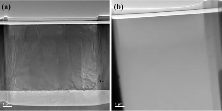
Figure 1 shows the cross-sectional transmission electron microscopy images of grown InGaN-based UV LEDs structures on (a) sapphire and (b) FS GaN substrate, respectively. When substrate of InGaN-based UV LEDs was changed from sapphire to FS-GaN, it can be clearly found that the crystallography of GaN epilayers was drastically different from that GaN epilayers on sapphire. It is well known that GaN epilayers grown on sapphire with two steps exhibit a high dislocation density. There are three types of dislocations in GaN including edge ( ), screw ( ), and mixed ( ). The dislocation density of InGaN-based UV LEDs on sapphire can be directly measured by transmission electron microscopy, but the samples on FS GaN substrate can’t be measured. So X-ray diffraction (XRD) is alternatively used as another method. The dislocation density (TD) can be calculated by the formula [13]:
(1)
where β is the FWHM measured by XRD rocking curves and b is Burgers vector length (bedge = 0.3189 nm, bscrew =
0.5185 nm). According to early study [14], the total defect densities of grown UV LEDs on FS-GaN and sapphire including edge, screw and mixed type were 3.6×106 cm-2 and 5.5×108 cm-2. From the results, we can conclude that the crystalline quality of InGaN-based UV LEDs structure on FS GaN substrate was better than on sapphire. Thus in this study was expected that 380 nm UV LEDs on FS GaN substrate have better internal quantum efficiency than on sapphire.
Proc. of SPIE Vol. 8986 898629-2
pen ...
IiI:GaN,we11:
.1
I
I
Microstructures or In -cluster
2 T111A1GaN barrier
T g = 0002
(b)
tiniAlGäN ararrier
InGGaN well
1
A1GaN barrier
T0002
Figure 1 (a) and (b) show the cross-sectional TEM images of grown InGaN-based UV LEDs on sapphire and FS-GaN substrate.
To better understand the crystal quality in the MQWs of grown InGaN-based UV LEDs on sapphire and FS GaN substrate, respectively, the high resolution TEM (HRTEM) images of InGaN/AlGaN MQWs region was performed as shown in figure 2 (a) and (b). When substrate of UV LEDs was changed from sapphire to FS-GaN, it can be clearly found the microstructures or indium-clustering can be not observed at UV LEDs on FS-GaN from HRTEM measurement. On the other hand, even the two samples since they were grown in the same run, the growth temperature of InGaN/AlGaN MQWs on sapphire and FS GaN substrate were different due to their different thermal conductivities, which influence indium-clustering itself and thereby emission light wavelength or output power resulting in thermal effect.
Figure 2 (a) and (b) shows the HRTEM image in InGaN/AlGaN MQWs structure of grown InGaN-based UV LEDs on sapphire and FS GaN substrate.
Proc. of SPIE Vol. 8986 898629-3
Carrier density ( # /cm')
1E15 1E16 1E17
1.0- 0.80.6 - O.4(I.2 -UVLED on Sapphire IQE= 39.4% RT LT (I.1 1'U\\ l'I'( cm-10 1.0- 0.8- 0.60.4 - 0.2-Carrier density ( # /cm')
1E15 1E16 1E17
0.0 UVLED on Gal IQE= 34.8% RT LT Power (A/cm) 10
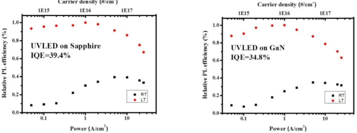
In order to clarify the indium-clustering in the MQWs of InGaN-based UV LEDs, the power-dependent PL measurement was performed. A general approach to evaluate the internal quantum efficiency (IQE) of near-UV LEDs is to compare PL-integrated intensity between low and room temperatures.[15] It could first transfer injected power to carrier density in the following equation:
Injected carrier density =
(2)
where P is the power of laser pumping, h is the Planck constant, is the frequency of laser. Hence h is the injected photon energy and is the spot size of laser pumping. The thickness of GaN and active region, dGaN and dactive, f related
to the repetition rate of laser pumping, the absorption efficiency of GaN and InGaN, αGaN and αInGaN, and the reflectance
of laser pumping denote by R. Here, it ignores the absorption of GaN due to the energy of laser pumping photons is less than its energy bandgap. The IQE curve fitting in this study is defined as the collected photon numbers divided by the injected photon numbers and normalized to the maximum efficiency of low temperature which shown in the following equation:
(3)
where C is constant including carrier injection efficiency and light extraction etc, ICol is the collected light intensity, IInj is
the injected laser intensity, ECol is the collected photon energy, and EInj is the injected photon energy. It ignores the
non-radiative recombination at low temperature (15K), therefore the peak of PL at low temperature correspond to IQE equal to 100%. Figure 3 shows the measured IQE as a function of excitation power at 15K and 300K for InGaN-based UV LEDs on sapphire and FS GaN substrate. At 20 mW of excitation power, it could be found that the IQE for InGaN-based UV LEDs on sapphire is corresponding with 4.6% enhancement than UV LEDs on FS GaN substrate. At this excitation level, we could calculate the corresponding generated carrier densities to be 2 × 1017 cm-3, approximately the same level of 20 mA at room temperature in UV LEDs. Thus higher internal quantum efficiency is in the UV LEDs grown on sapphire substrate due to the indium-clustering in the MQWs of InGaN-based UV LEDs.
Figure 3 shows the measured IQE as a function of excitation power at 15K and 300K for InGaN-based UV LEDs on sapphire and FS GaN substrate.
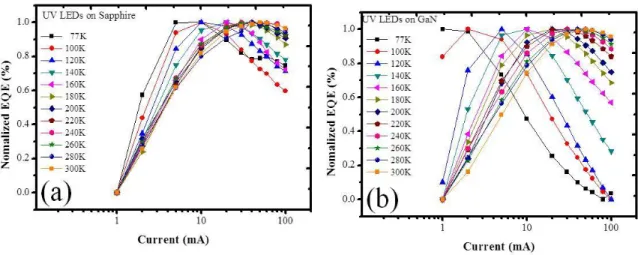
In spite of the IQE enhancement of InGaN-based UV LEDs on FS GaN substrate have not been expected because of influence of indium-clustering in the MQWs, the indium-clustering in MQWs is the defect. Thus the defect-induced Auger recombinations of efficiency droop may be observed in the electroluminescence measurement.Figure 4 (a) and (b) plot the EQE as a function of injected current for InGaN-based UV LEDs on sapphire and FS GaN substratre, respectively, from 77 K to 300 K. The EQE is equal to (P/hν)/(I/e) = ηintηLEE. The maximum EQE of InGaN-based UV
LEDs generally were observed to increase with increasing temperature. When substrate of InGaN-based UV LEDs was changed from sapphire to FS-GaN, it can be clearly found the different in the efficiency behavior and the droop behavior. The maximum values of external quantum efficiency in UV LEDs on FS GaN substrate were better than on sapphire due to it still have high efficiency at 77 K to 100 K. Besides, the droop behaviors of UV LEDs on sapphire and FS-GaN substrate were drop from 77 K to 280 K, and steady from 280 K to 300 K. All in all, the InGaN-based UV LEDs on FS
Proc. of SPIE Vol. 8986 898629-4
e
= Z - 77K -II- 100K -4- 120K -v-- 140K - 4- 160K T 180K - 200K - a- 220K - 0- 240K -*-- 260K -11.- 280K - 300K 1 10 100 Current (mA) 1.00.8 -, 0.6-k? 0.4-0.2. Z 0.0-LT' LÈDs ori Gesti- 77K
-4- 100K -4- 120K rt- 140K T 160K - 10- 180K -V- 200K -- 220K f 240K -Jr- 260K - 0- 280K + 300K(b)
1 10 Current (mA) 100 2422-
20- 18-,-,16-v
14-á
12- 10-8 6 4 UV LEDs on Sapphire UV LEDs on ES-GaN3%
20%
20 40 60 80 100Current (mA)
GaN substrate have a better well in quality which it can contain more carriers. But the efficiency droop behaviors in InGaN/AlGaN MQWs on sapphire and FS GaN substrate were effect by thermal effect in MQWs.
Figure 4 shows the temperature dependent EL of the grown InGaN-based UV LEDs on (a) sapphire and (b) FS GaN and sapphire.
The EQE of grown InGaN-based UV LEDs on sapphire and FS GaN substrate were shown in figure 5 at the same wavelength of 380 nm. The InGaN-based UV LEDs on FS GaN substrate present better behavior in decreasing efficiency droop than on sapphire. From this sample with 3% efficiency droop, it was attributed to decreasing Auger recombination loss in this study because of InGaN/AlGaN MQWs without indium-clustering.
Figure 5 shows the L-I-V and efficiency droop of the grown InGaN-based UV LEDs on FS GaN and sapphire.
To gain a better understanding of the reason of efficiency droop and carriers loss mechanism, simple ABC model was used that EQE of InGaN-based UV LEDs as expressed by:[16]
(4)
where A is Shockley-Read-Hall (SRH) nonradiative recombination coefficient, B is the radiative recombination coefficient, and C is the Auger nonradiative recombination coefficient, respectively. Eext represents extraction efficiency
and n is the carrier density. It could be seen from Eq. (4), the coefficients A, B, and C, respectively, is the key factor to investigating the carrier loss in different recombination mechanisms and efficiency droop in InGaN/AlGaN UV LEDs. General speaking, in this simple model, the influence of Shockley-Read-Hall (SRH) nonradiative and radiative
Proc. of SPIE Vol. 8986 898629-5
coefficients may not be clearly. Thus recent researches trend to Auger recombination loss. In this study, it was reasonable to assume that there should be some intrinsic relationship between defect densities including indium-clustering, Auger recombination, and the dramatic decrease in external quantum efficiency at high excitation, considering significantly indium-clustering of the MQWs in these devices. To solve efficiency droop of InGaN-based UV LEDs, decreasing the defect densities in the LEDs structure is an important challenge. Choosing FS GaN substrate for UV LEDs structure growth is attributed to next generation technique because of low defect density (106 cm-2) to obtain the high efficiency and low droop in the InGaN-based UV LEDs at the same time.
4. SUMMARY
In this study, we observe the relationship of indium clustering and efficiency droop in ultraviolet light-emitting diodes via TEM, the power dependent photoluminescence, and temperature dependent electroluminescence measurement. In spite of the indium clustering in MQWs of UV LEDs could improve the internal quantum efficiency, the performances of light output power and efficiency droop of 12 mil square UV LEDs chips on FS-GaN substrate still surpass than UV LEDs with indium clustering. The efficiency droop of UVLEDs on FS-GaN decrease to 3 % than UV LEDs with indium clustering.
REFERENCES
[1] A. Khan, K. Balakrishnan, T. Katona, “Ultraviolet light-emitting diodes based on group three nitrides”, Nat. Photonics 2 (2), 77 (2008)
[2] G. Tamulaitis, “Ultraviolet light emitting diodes”, Lithuanian J. Phys. 51 (3), 177 (2011)
[3] T. H. Seo, K. J. Lee, A. H. Park, C. H. Hong, E. K. Suh, S. J. Chae, Y. H. Lee, T. V. Cuong, V. H. Pham, J. S. Chung, E. J. Kim, S. R. Jeon, “Enhanced light output power of near UV light emitting diodes with grapheme/ indium tin oxide nanodot nodes for transparent and current spreading electrode”, Opt. Express 19 (23), 23111 (2011)
[4] Y. Narukawa, Y. Kawakami, M. Funato, S. Funato, S. Nakamura, “Role of self-formed InGaN quantum dots for exciton localization in the purple laser diode emitting at 420 nm”, Appl. Phys. Lett. 70, 981 (1997)
[5] C. Kisielowski, Z. Liliental-Weber, S. Nakamura, “Atomic Scale Indium Distribution in a GaN /In0.43Ga0.57N
/Al0.1Ga0.9N Quantum Well Structure”, Jpn. J. Appl. Phys. 36, 6932 (1997)
[6] H. K. Cho, J. Y. Lee, J. H. Song, P. W. Yu, G. M. Yang, C. S. Kim, “Influence of strain-induced indium clustering on characteristics of InGaN/GaN multiple quantum wells with high indium composition”, J. Appl. Phys. 91 (3), 1104 (2002)
[7] I. Gorczyca, S. P. Lepkowski, T. Suski, N. E. Christensen, A. Svane, “Influence of indium clustering on the band structure of semiconducting ternary and quaternary nitride alloys”, Phys. Rev. B 80 (7), 075202 (2009)
[8] K. H. Baloch, A. C. Johnston-Peak, K. Kisslinger, E. A. Stach, S. Gradecak, “Revisiting the In-clustering question in InGaN through the use of aberration-corrected electron microscopy below the knock-on threshold”, Appl. Phys. Lett. 102 (19), 191910 (2013)
[9] M. H. Kim, M. F. Schubert, Q. Dai, J. K. Kim, E. F. Schubert, J. Piprek, Y. Park, “Origin of efficiency droop in GaN-based light-emitting diodes”, Appl. Phys. Lett. 91 (18), 183507 (2007)
[10] X. Ni, Q. Fan, R. Shimada, U. Ozgur, H. Morkoc, “Reduction of efficiency droop in InGaN light emitting diodes by coupled quantum wells”, Appl. Phys. Lett. 93 (17), 171113 (2008)
[11] Y. C. Shen, G. O. Mueller, S. Watanabe, N. F. Gardner, A. Munkholm, M. R. Krames, “Auger recombination in InGaN measured by photoluminescence”, Appl. Phys. Lett. 91 (14), 141101 (2007)
[12] A. Y. Kim, W. Gotz, D. A. Steigerwald, J. J. Wierer, N. F. Gardner, J. Sun, S. A. Stockman, P. S. Martin, M. R. Krames, R. S. Kern, F. M. Steranka, “Performance of High Power AlInGaN Light Emitting Diodes”, Phys. Status Solidi A 188 (1), 15 (2001)
Proc. of SPIE Vol. 8986 898629-6
[13] C. G. Dunn, E. F. Koch, “Comparison of dislocation densities of primary and secondary recrystallization grains of Si-Fe”, Acta Metall. 5, 548 (1957)
[14] C. Y. Shieh, Z. Y. Li, C. H. Chiu, P. M. Tu, H. C. Kuo, G. C. Chi, “Influence of free-standing GaN substrate on ultraviolet light-emitting diodes by atmospheric-pressure metal-organic chemical vapor deposition”, Proc. Of SPIE 8625, 862525 (2013)
[15] S. Watanabe, N. Yamada, M. Nagashima, Y. Ueki, C. Sasaki, Y. Yamada, T. Taguchi, K. Tadatomo, H. Okagawa, H. Kudo, “Internal quantum efficiency of highly-efficient InxGa1-xN-based near-ultraviolet light-emitting diodes”,
Appl. Phys. Lett. 83 (24), 4906 (2003)
[16] Z. Liu, T. Wei, E. Guo, X. Yi, L. Wang, J. Wang, G. Wang, Y. Shi, I. Ferguson, J. Li, “Efficiency droop in InGaN/GaN multiple-quantum-well blue light-emitting diodes grown on free-standing GaN substrate”, Appl. Phys. Lett. 99 (9), 091104 (2011)
Proc. of SPIE Vol. 8986 898629-7