Diffusion and crystallization mechanisms of Ge/ Au bilayer media
for write-once optical disk
T. H. Wu, P. C. Kuo,a兲 and S. L. Ou
Institute of Material Science and Engineering, National Taiwan University, Taipei 106, Taiwan Jung-Po Chen, Po-Fu Yen, and Tzuan-Ren Jeng
Electronics and OptoElectronics and Research Laboratories, Industrial Technology Research Institute, Hsinchu 310, Taiwan
Chih-Yuan Wu
Department of Physics, Fu Jen Catholic University, Hsinchuang 242, Taiwan Der-Ray Huang
Hsinchu Science Based Industrial Park, Hsinchu 300, Taiwan
共Received 7 August 2007; accepted 14 December 2007; published online 10 January 2008兲 Ge/Au bilayer thin films were fabricated by magnetron sputtering method, the temperature dependence of resistance from room temperature to 500 ° C and concentration depth profiles are measured. From the temperature dependence of resistance measurement, we found two phase change phenomena which occurred at 175 and 360 ° C. The element concentration depth profiles of the as-deposited and recorded region indicate that the Au–Ge alloy is initially formed at the Ge/Au interface. The dominant diffusion element is Au atom and the diffusion path is from Au layer to Ge layer. The optimum simulated bit error rate value is about 1.4⫻0−6at 9.0 mW under two time high definition digital versatile disk共HD DVD兲 recording speed. The dynamic tests show that this Ge/Au bilayer films can be applied to one to two times HD DVD-R. © 2008 American Institute of Physics. 关DOI:10.1063/1.2831690兴
Recently, the optical disk was improved due to the needs of large information transformation and high definition me-dia resolution. Blu-ray disc共BD兲 and high definition digital versatile disk共HD DVD兲 had been proposed as the promis-ing candidates. Various inorganic recordpromis-ing media were re-ported for them. The jitter value of Bi–Ge nitride1was found only 5.7% under 36– 72 Mbps writing speed. Te–O–Pd共Ref.
2兲 was proposed as a four layer recording media for
100 Gbyte BD system. The bilayer structure, such as amor-phous silicon 共a-Si兲/metal3–6 have also been studied. Al-though the relationship between microstructure and anneal-ing temperature of a-Ge/Au had been discussed previously,5 the diffusion mechanism of Ge/Au bilayer during recording is not identified.
In this paper, the diffusion and crystallization mecha-nisms of a-Ge/Au bilayer media for write-once HD DVD disks are investigated. Two steps of phase change are found by measuring the variation of electrical resistance with tem-perature. The element concentration depth profiles of the as-deposited and recorded region, which were measured by Au-ger electron spectrometer共AES兲, indicate that the diffusion path was from Au layer to Ge layer.
The resistance of Ge/Au bilayer with nature oxidized 共110兲 silicon wafer substrate was measured by the four-probe resistance tester in vacuum. Figure 1共a兲 shows the layer structure of the sample. The a-Ge共10 nm兲/Au共10 nm兲 bi-layer for AES investigation was prepared by magnetron sput-tering on polycarbonated 共PC兲 substrate, as shown in Fig.
1共b兲. The sample with PC substrate was then laser initialized, and the variation of its reflectivity with wavelength was
mea-sured by spectrometer共ETA-RT, Optik’s high sensitive spec-trometer兲. The initialized sample, which has the largest opti-cal contrast at=405 nm 共comparing with the as-deposited sample兲, is selected for the AES measurement. The element concentration depth profile was measured by AES with sput-tering speed of 0.2 nm/s. The recording characteristics were evaluated by dynamic tester共ODU1000, PULSTEC兲, which the testing conditions are shown in TableI.
a兲Author to whom correspondence should be addressed. Tel.: ⫹886-2-23648881. Fax:⫹886-2-23634562. Electronic mail: [email protected].
FIG. 1. The layer structure of samples for共a兲 resistance measurement and 共b兲 AES depth profile measurement.
APPLIED PHYSICS LETTERS 92, 011126共2008兲
0003-6951/2008/92共1兲/011126/3/$23.00 92, 011126-1 © 2008 American Institute of Physics
Figure2shows the variation of resistance with tempera-ture. The Ge/Au bilayer film has two phase transformation temperatures which are 175 and 360 ° C. The first phase change temperature corresponds to the interdiffusion of the bilayers.5Since the probes touch the surface of Au layer, as shown in Fig. 1共a兲, the measured resistance represents Au layer’s behavior. The resistance increases with decreasing Au layer’s thickness共Ohm’s law, R=L/A, where= resistivity, L = sample length, and A = cross sectional area兲. The expan-sion of Ge/Au interface layer and the new forming discon-tinuous phase by interdiffusion of Au and Ge atoms resulted in the rising of resistivity at 175 ° C. So, the crystallization temperature of Ge is decreased from 473共Ref.7兲 to 175 °C.
This mechanism is called the metal induced crystallization 共MIC兲 mechanism.3–6,8
From the observation of high resolu-tion transmission electron microscope,5rearranging atoms of the breaking of Au–Ge bonds and precipitation of Ge were found at 340 ° C. However, from our resistance measure-ment, it shows no further phase change higher than 175 ° C, until the temperature approaches to the eutectic temperature of Ge/Au 共363 °C兲.9
This owes to the low solubility of Au in crystalline Ge共13.6 ppm兲,10the metal induced crystallites of Ge hinder the further diffusion of Au into Ge at tempera-ture between 175 and 360 ° C, until the temperatempera-ture ap-proaches to the eutectic temperature of Ge/Au 共363 °C兲, the Ge/Au films show another phase transformation.
In order to identify the atom’s migration direction be-tween Au and Ge layers during diffusion, the element depth profiles of as-deposited and recorded samples were measured by AES. Figure3shows the depth profile of Ge/Au bilayer.
The total sputtering time is 100 s, which corresponds to about 20 nm depth from the surface. The film was composed
by three layers, which are the Au layer, the Ge/Au interface layer, and the Ge layer. Significantly, the Au–Ge interlayer was formed initially. In 1989, Hou et al.11had discussed the heterogeneous nucleation and the random found limited mass transport at Au/Ge interlayer. In our examination, the diffu-sion path has been further revealed
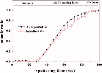
Figures4 and5 are the Ge and Au concentration depth profiles of as-deposited and laser initialized in the Ge/Au bilayers, respectively. During the first 30 s of the sputtering 共about 0–6 nm depth兲, the two curves in Fig.4 remain ex-tremely low. The Ge atoms did not diffuse to such depth after laser initialized. However, between 30 and 40 s 共about 6 – 8 nm depth兲, the Ge concentration in laser recorded sample is slightly larger than that of the as-deposited sample. After that, although these two curves increase with the depth, the Ge concentration of laser initialized sample is lower than that of as-deposited sample. On the other hand, the Au atoms diffused into Ge layer as the depth deeper than 16 nm 共sput-tering time is longer than 80 s兲, as shown in Fig. 5. At the sputtering time of 30– 40 s 共about 6–8 nm depth兲, the Au concentration of laser recorded sample is slightly smaller than that of the as-deposited sample. These two curves de-crease further as the sputtering time is inde-creased again. How-ever, the Au concentration of laser initialized sample is higher than that of as-deposited sample at sputtering time of 40– 80 s共depth of 8–16 nm兲. Those results indicate that the Ge atoms did not obviously diffuse to the Au layer, the domi-nant diffusion element is Au and the diffusion path is from Au layer to Ge layer during recording. Au–Ge bonds were formed by Au interdiffusion. The broken metastable Au–Ge bonds were established during recording facilitated the local rearrangement.12Since the solubility of Au in crystallized Ge is low, the Au atoms will be squeezed out as the Ge crystal-lizes growing. The dependence between the metal thickness and the a-Ge layer was discussed.13 The MIC mechanism only affected the metal/a-Ge interface which was located
FIG. 3. 共Color online兲 The concentration depth profile of as-deposited and laser initialized Ge/Au bilayer samples.
TABLE I. Dynamic test conditions. User capacity Thickness of substrate Wavelength Numerical aperture共NA兲 Modulation code Track pitch Channel clock frequency Linear velocity User bit rate 15 GB 0.6 mm 405 nm 0.65 ETM, RLL 共1,10兲 0.4m 64.8 Mhz 13.2 m/s 73.1 Mbps
FIG. 2. Relationship between the electric resistance and temperature of Ge/Au bilayer.
011126-2 Wu et al. Appl. Phys. Lett. 92, 011126共2008兲
close to the bilayers. By the AES result, the diffusion limi-tation is revealed. Au atoms diffused into 8 nm depth of Ge layer, which resulted in the optical contrast between as-deposited and laser pulsed state.
Figure 6 shows the simulated bit error rate 共SbER兲 value5 and the modulation of the Ge/Au bilayer compared with the laser powers. The SbER value is decreased from 1.2⫻10−5to 1.4⫻10−6as the writing power increased from
8.3 to 9.0 mw, and then further increased to 2.0⫻10−5as the
writing power increased to 9.6 mw. Meanwhile, the modula-tion is about 0.77–0.78. SbER value was suggested to be lower than 1⫻10−5. The optimum SbER value in our
dy-namic test is 1.4⫻10−6 which occurred at about 9.0 mW
under two times HD DVD recording speed that means the Ge/Au bilayer recording thin film is suitable for two times HD DVD write-once disk.
In summary, recording properties of a-Ge/Au write-once optical media had been studied. From the four-probe resistance measurement, it is found that the crystallization temperature of Ge will be reduced from 473 to 175 ° C by the interdiffusion of Au atoms. The AES inspection proves that the dominant diffusion element is Au and the diffusion path is from Au layer to Ge layer during recording. Dynamic tests show that the optimum SbER is 1.4⫻10−6 which
oc-curred at about 9.0 mW under two times HD-DVD recording speed.
This work was supported by the National Science Coun-cil and Ministry of Economic Affairs of Taiwan through Grant Nos. NSC 95-2221-E-002-115 and 95-EC-17-A-08-S1-0006.
1Y. Hosoda, T. Izumi, A. Mitsumori, F. Yokogawa, S. Jinno, and H. Kudo, Jpn. J. Appl. Phys., Part 1 42, 1040共2003兲.
2K. Kimura and E. Ohno, Jpn. J. Appl. Phys., Part 1 28, 2223共1989兲. 3Y. C. Her, S. T. Jean, and J. L. Wu, J. Appl. Phys. 102, 093503共2007兲. 4H. Inoue, K. Mishima, M. Aoshima, H. Hirata, T. Kato, and H.
Ut-sunomiya, Jpn. J. Appl. Phys., Part 1 42, 1059共2003兲.
5T. H. Wu, P. C. Kuo, J.-P. Chen, C.-Y. Wu, P.-F. Yen, T.-R. Jeng, D.-R. Huang, and Y.-H. Fang, Appl. Phys. Lett. 90, 151111共2007兲.
6Y.-C. Her, C.-W. Chen, and C.-L. Wu, J. Appl. Phys. 99, 113512共2006兲. 7F. Oki, Y. Ogawa, and Y. Fujiki, Jpn. J. Appl. Phys. 8, 1056共1969兲. 8S. W. Russell, J. Li, and J. W. Mayer, J. Appl. Phys. 70, 5153共1991兲. 9Binary Alloys Phase Diagrams, 2nd ed., edited by B. Thaddeus, J. L.
Murray, L. H. Bennett, and H. Baker共American Society for Metals, Met-als Park, OH, 1986兲, Vol. 1, p. 373.
10H. Okamoto and T. B. Massalski, Bull. Alloy Phase Diagrams 5, 601 共1984兲.
11J. G. Hou, Z. Q. Wu, and L. S. Bi, Thin Solid Films 77, 173共1989兲. 12Z. Tan, S. M. Heald, M. Rapposch, C. E. Bouldin, and J. C. Woicik, Phys.
Rev. B 46, 9505共1992兲.
13G. Radnoczi, A. Robertsson, H. T. G. Hentzell, S. F. Gong, and M.-A. Hasan, J. Appl. Phys. 69, 6394共1991兲.
FIG. 4. 共Color online兲 The concentration depth profile of as-deposited and laser initialized Ge atoms in the Ge/Au bilayer samples.
FIG. 5. 共Color online兲 The concentration depth profile of as-deposited and laser initialized Au atoms in the Ge/Au bilayer samples.
FIG. 6. SbER value and modulation of the Ge/Au bilayer medium as a function of writing power. The track pitch is 0.4m.
011126-3 Wu et al. Appl. Phys. Lett. 92, 011126共2008兲