Boundary Effects on the Optical Properties of
InGaN Multiple Quantum Wells
L.-H. Peng, Member, IEEE, C.-M. Lai, C.-W. Shih, C.-C. Chuo, and J.-I. Chyi
Abstract—We examine the issues of spontaneous and piezo-electric polarization discontinuity on the optical properties of 3.0-nm-thick indium gallium nitride (InGaN) multiple quantum wells (MQWs). A quench of band-edge emission from the cap GaN layer is observed when the photoexcitation source is changed from a 355- to a 248-nm laser. The interband transitions from the InGaN wells exhibit a linear dependence on the 1) spectral blue shift of 8.5 10 18 meV cm3 and 2) change of the internal field of 3 10 14V cm2 with the injected carrier density up to Ninj 1019 cm 3 at 77 K. These observations are attributed to the redistribution of photogenerated carriers in the InGaN wells due to the polarization discontinuity at the QW interface and the surface band bending effect. By incorporating an additional boundary condition of surface Fermi-level pinning into the Poisson equation and the band-structure analysis, it is shown the emission from the InGaN–GaN MQWs is dominant by the recombination between the high-lying subbands and the screening of internal field effects.
Index Terms—Fermi-level pinning, indium gallium nitride mul-tiple quantum wells (InGaN MQWs), polarization effects.
I. INTRODUCTION
T
HE WIDE bandgap III–V nitrides have long been rec-ognized as a material of outstanding optical, electronic, and thermal properties compared with their counterparts of in the group IV and II–VI compounds [1]. This has led massive nitride research activities in optoelectronics and high temper-ature/power electronics [2]. The recent commercialization of candela class indium gallium nitride (InGaN) blue/green light-emitting diodes and long lifetime violet and blue laser diodes represent one such exciting achievement [3]. High-gain opera-tion of the GaN-based field effect transistors in the GHz regime has thrived their use for power electronics applications [4]. De-spite progress has been made in the material growth and device processing, the mechanism responding to these novel device functionality still remains a great mystery to be resolved. For example, the origin for the formation of two-dimensional elec-tron gas (2-DEG) at the undoped AlGaN–GaN interface and the corresponding high electronic mobility effects are still unclear [5]. Piezoelectric doping [6] represents one such possibility but surface defect can also account for a plausible argument [7]. On the other side of optical device analysis, while a prevailingManuscript received December 18, 2002; revised June 11, 2003. This re-search was supported by the NSC under Grant 90-2215-E-002-017.
L.-H. Peng, C.-M. Lai, and C.-W. Shih are with the Department of Electrical Engineering and Institute of Electro-Optical Engineering, National Taiwan Uni-versity, Taipei, Taiwan, R.O.C.
C.-C. Chuo and J.-I. Chyi are with the Department of Electrical Engineering, National Central University, Chung-Li, Taiwan, R.O.C.
Digital Object Identifier 10.1109/JSTQE.2003.818855
theory suggests the emission mechanism to the localized states in InGaN [8], the discontinuity of piezoelectricity and spontaneous polarization at the nitride interface [9] can also respond to the change of oscillator strength in the spectral analysis.
A popular approach in the nitride device mod-eling is to incorporate a periodical field distribution of in the band-structure analysis [10]. The polarization-induced field of and , therefore, has opposite sign and scales inversely with the length of well and barrier , respectively. The discontinuity of and at the nitride/air interface, however, imposes a disturbance on the boundary condition since a relatively large charge density of 2 10 cm can reside at the nitride surface [11]. This, in turn, would affect the analysis of the electronic and optical properties when device modeling of a nitride heterostructure comes into concern [12]. Based upon an observation of Fermi-level pinning at the surface of nitride layer [13], a more recent treatment is to invoke a donor-like surface state to compensate the inadvertent surface charge [14]. In thermal equilibrium, charge neutrality associated with the lineup of Fermi level across the AlGaN–GaN heterostructure determines the amount of free carrier released from the ionized surface state, and, therefore, affect the transport properties of the device [15].
These observations suggest a fundamental approach to the nitride device modeling would be to incorporate the polariza-tion-induced charge and surface Fermi-level pinning in the band-structure analysis. In order to simulate the effects of carrier redistribution upon device operation, one has to cope with, in addition to analyze the conduction band Schrödinger and valence Rashba–Sheka–Pikus (RSP) Hamiltonian [16], the solutions from the Poisson and rate equations. As a result, the capability of treating the perturbations of polarization-induced charge, field screening, band filling, and bandgap renormaliza-tion on an equal footing marks the essence of this work. Here, we use a series of selective wavelength excitation experiments to examine the boundary effects on the optical properties of InGaN–GaN multiple quantum wells (MQWs). We thereby are able to observe the transportation of photogenerated carriers from the GaN cap layer and their redistribution and radiative combination in the adjacent InGaN wells. We find it essential to include the Fermi-level pinning as an additional boundary condition in the band-structure analysis to resolve the carrier redistribution effects in the nitride heterostructure. Our analysis indicates the emission properties of the 3.0-nm InGaN MQWs are due to the dominant transitions between the high-lying subbands and the screening effects on the internal field.
II. EXPERIMENTS
The MQWs samples used in this study were grown by the metalorganic chemical vapor deposition (MOCVD) technique. The detailed growth procedure and material characterization can be found in [17]. The sample structures consisted of, in se-quence, an undoped 30- or 50-nm GaN cap layer with three pairs of 3.0-nm In Ga N–GaN MQWs with a silicon doping concentration of 10 cm , and a 1.5- m-thick GaN buffer layer of cm background doping on the (0001) face of sapphire substrates. The In composition ( and 0.18) in the well and thickness in the GaN barrier ( and 7 nm) were varied to examine the distribution of internal field effect on the optical properties. Note the corresponding piezo-electric polarization field for nitride heterostructures grown on the (0001) face follows that of (A4). If the nitride heterostruc-ture is grown on a (000-1) face, the polarization field would be opposite to that shown previously [5].
The use of a thin GaN cap layer is crucial since it allows the generation of photo-carriers to be selectively “imbedded” to a region approximately equal to the absorption length of the nitride material at a given ultraviolet wavelength. The selective wavelength excitation experiments were performed by using a third-harmonic generation (355 nm) of Nd:YAG laser (New Wave, Freemont, CA) and a 248-nm KrF excimer laser (TuiLaser, Munich, Germany) with a maximum energy of 15 mJ. The lasers have a pulsewidth of 10 ns and are typically operated at a repetition rate of 10 Hz. The samples were mounted in a low-temperature cryostat (CTI-cryogenics, Waltham, MA) and the photoluminescence (PL) signals were collected from the sample surface, dispersed by a grating spectrometer, and detected by a charge coupled device array.
III. RESULTS ANDDISCUSSION A. Optical Characterization
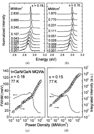
We illustrate in Fig. 1 the emission spectra measured at 77 K from the 3.0 nm (a) and (b) In Ga N–GaN MQWs as excited by the 355-nm Nd:YAG laser. We first note a slant V-like move in the peak emission energy as a function of the laser excitation intensity. A clear shift of 70 meV in the peak emission energy can be identified as one changes from a low to high In-content InGaN MQWs. Note the emission spectra reveal a blue shift ( 80 meV) upon the increase of pump inten-sity till a threshold ( 0.1 MW/cm at 77 K) is reached. One can further infer from Fig. 1 an abrupt change on the slope of the integrated peak emission intensity, i.e., from a linear- into square-power dependence as the excitation density exceeds the threshold. In concurrence with this threshold behavior on emission intensity is a spectral linewidth narrowing as the pump intensity varies from 0.1 to 1 MW/cm . Note in this regime the InGaN MQW’s emission only exhibits a slight spectral red shift ( 15 meV). These observations typically signify an onset of stimulated emission [18]. However, whether the underlying mechanism is due to localized states or electron-hole plasma recombination is still under debate [19]. With further increase of the pump intensity into the high-density excitation regime, the InGaN MQWs emission resumes a spectral red shifting and broadening due to a contribution from the electron-hole plasma
Fig. 1. The 77-K PL spectra of the (a)x = 0:15 and (b) x = 0:18 3.0-nm In Ga N–GaN MQWs excited by a 355-nm Nd:YAG laser. The spectra have been vertically shifted for comparison.
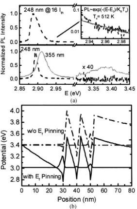
[20] and the associated bandgap renormalization [21] and/or heating effects [22]. Data shown in Fig. 2(a) reveals one such example of carrier heating with a characteristic exponential tail on the high-energy side (i.e., from 2.94 to 3 eV) of the spectrum as the excitation density of the 248-nm laser at room tempera-ture exceeds 16 . On the other hand, increase of the measure-ment temperature to 300 K [23] only results in an increase of the threshold density 1 MW/cm and renders a sim-ilar spectral evolution except a 30-meV decrease in the peak emission energy.
A general assumption in the optical analysis is that the recom-bination is governed by the localized states at low temperature, whereas at high temperature, it is controlled by the extended states [24]. However, our observation of constant emission peak energy in the low-density excitation ( 10 MW/cm , not shown in Fig. 1 but can be seen in Fig. 6) regime, which is in-dependent of the measurement temperature, suggests the state of localization has been minimized in the samples under study. Were this not the case, the filling of localized or band tail states by the photogenerated carriers would quickly raise the emission energy. Note similar phenomenon of constant peak energy has also been recently reported on the room-temperature emission spectra of a wider 4-nm-thick In Ga N–GaN MQWs [25]. We further note the temperature dependence of the peak energy shift, as inferred from the low-density 10 10 MW/cm excitation experiments and to be discussed in Section III-D, only reaches half of the value as would expect from the Varshni ef-fect. Including the localization effect, however, would only
in-Fig. 2. (a) The 300-K PL spectra of the In Ga N–GaN MQWs excited by the 355- and 248-nm lasers near threshold intensity at 1.2I . The GaN emission has been magnified by 40 times in both cases. Note the spectrum taken at far above threshold (l6I ) exhibits the carrier heating effect. (b) Band-edge profiles of the In Ga N/GaN MQWs analyzed with and without Fermi-level pinning at the GaN surface layer.
crease rather than decrease the energy difference [26]. These observations suggest the dominant emission mechanism of this study is not limited by the localized state.
To cope with a model analysis that can genuinely reflect the distribution of photogenerated carrier in the InGaN–GaN MQWs, we seek information from the results of selective wavelength excitation experiments. We take advantage of the large absorption coefficient of nitride in the shorter wavelength regime to render a majority of photogenerated carriers in the GaN cap layer [27]. The effective absorption length is estimated to be about and decrease with the shorter laser wavelength. Since the pulsewidth of the excitation lasers ( 10 ns) is larger than a typical relaxation time observed in GaN ( 1 ns), in the following discussion, we consider the luminescence is derived from the steady-state response [28]. Referring to Fig. 2(a), one notes the emission intensity from the GaN cap layer at 3.4 eV is considerably lower than that from the InGaN well at 2.9 eV, only reaching 1% of the peak value in the latter as excited by the 355 nm laser. However, by changing the excitation source to a 248-nm laser, we find emission from the GaN cap layer ceases but that from the InGaN well prevails. This occurs in an excitation density range from 10 to 10 MW/cm and reflects a subtlety of radiative combination mechanism in this InGaN–GaN MQWs system. Were the photogenerated carriers to have a similar probability to be captured in the GaN cap layer/barrier and the InGaN well, the peak ratio of the corresponding PL intensity should stay about the same and independent of the excitation wavelength.
Fig. 3. Comparison of the experimental PL peak energy of the In Ga N–GaN MQWs with those calculated with and without surface Fermi-level pinning.
Our experimental observations, however, do not support the above argument but suggest the band structure in the GaN cap layer and InGaN MQWs, and the accompanying field distribution play an important role in determining the emission characteristics.
B. Theoretical Modeling
To quantify the previous observations, the equations of motion for the electron and hole in the nitride heterostructure, as stated in the Appendix, are solved consistently by a finite-difference method [29] that incorporates the steady-state solutions from the rate and Poisson equations to describe the generation and redistribution of the photo-carriers under the action of polarization-induced charge at each of the nitride interface, i.e., . To evaluate the bandgap renormalization effect, we adapt an important universal relation between the reduced bandgap energy and carrier density, i.e. , as recently reported by Park and Chuang [30]. Since the Fermi level pinning represents a genuine situation occurred to the undoped GaN surface, this phenomenon is assessed by a donor-like surface state with density 10 cm to ensure a pinning of at 0.4 eV below the conduction band edge of GaN. In the analysis, we let the Roosbroeck–Shockley radiative recombination coefficient B of GaN be the only fitting parameter and a temperature dependence following that in [31]. By doing so, the photogenerated carrier density to be injected into the MQW’s structure can be deduced from the absorbed laser intensity by solving a nonlinear equation of (A9). The injected carrier density, , which then becomes a fixed parameter, is used with other material parameters to compute the theoretical spectra shown from Figs. 3 to 7. The material parameters of InGaN are taken as a linear interpolation from those of the binary GaN and InN as listed in Table I [32], except the deformation potentials of InN are assumed to be the same as those of GaN and a bowing factor of 2.05 eV is used for calculating the bandgap energy of InGaN. The nonlinear dependence of the spontaneous and piezoelectric polarization with the alloy material composition [33], however, has been neglected for clarity purpose.
C. Boundary Effects
We depict in Fig. 2(b) the band-edge profiles of the 3.0 nm In Ga N–GaN MQWs correspond to the
Fig. 4. Calculated energy dispersion and emission spectra of the In Ga N–GaN MQWs under the case of (a) high (N = 7:6 2
10 cm ) and (b) low (N = 3:5 2 10 cm ) carrier injection at 77 K.
Fig. 5. Comparison of the experimental and calculated emission spectra of the 3.0 nm (a)x = 0:15 and (b) x = 0:18 In Ga N–GaN MQWs at 77 K.
boundary condition of (a) periodical field distribution with a flat surface and (b) surface Fermi-level pinning with polarization-induced charge of at each of the nitride interface, respectively. Note a common feature of these two model
Fig. 6. Comparison of the experimental and calculated peak emission energy as a function of injection carrier density(N ) for the (a) x = 0:15 and (b) x =
0:18 In Ga N–GaN MQWs at 77 K and 300 K. Inset: a linear change of the peak energy and internal field withN .
Fig. 7. Comparison of the experimental and calculated integrated PL intensity of the (a)x = 0:15 and (b) x = 0:18 In Ga N/GaN MQWs at 77 K.
analyses is the resultant saw-tooth like confinement potential in InGaN–GaN MQWs. However, the nonzero surface electric field in the GaN cap layer ( 0.17 MV/cm) reflects the local electrostatics due to the release of free carriers from the ionized surface states in the latter case.
These effects lead to several important considerations in the following bandstructure analysis. First of all, the steep incline of the GaN surface layer in case (b) can facilitate the transportation of photogenerated electron (hole) toward
TABLE I
MATERIALPARAMETERS FORGaNANDInN
the interior (surface) of the MQW structure. Whereas, a flat surface of case (a) without Fermi level pinning would leave the photogenerated carriers a similar capture probability in the GaN cap layer and in the InGaN well. The resultant difference is a red shift of 50 meV in the peak emission energy of case (a) with respect to that obtained with a surface Fermi-level pinning when the device is operated at cm at 77 K. More evidence is provided in Fig. 3 upon which the experimental emission peak energy of the In Ga MQWs in Fig. 1 are compared with that calculated by the above two models. For case (a), without surface Fermi-level pinning, one notes the peak energy cannot be fitted with a single set parameter of piezoelectric polarization , whereas, in the surface pinning model calculation, the experimental data can be well resolved by assuming a low-temperature (77 K) value of C/m . This observation clarifies the importance of pursuing the surface pinning model in the following band structure analysis. Secondly, we note the field strength ( 2 MV/cm) in the InGaN well, as inferred from the slope of the potential profile shown in Fig. 2(b), is far more
than that required for the dissociation of localized exciton [34]. This indicates that the temperature effects on the InGaN MQW emission characteristics of this study would be less influenced by the localized states. It also agrees with a recent study of InGaN–GaN QW [35], revealing a drastic reduction of the localized exciton due to the large internal field [36] and carrier screening effect [37].
Note that under a strong field action, not only can one encounter a reduced oscillator strength but also a relaxation of parity-selection rule, i.e., among the interband transitions [38]. Furthermore, the degenerate eigenstates from each of the composing InGaN–GaN MQWs of identical structure would encounter a finite mixing and anticrossing in the band structure dispersion as shown in Fig. 4. Indeed, the mixing effects are more pronounced in the (a) high injection cm than in the (b) low injection cm case. As a result, one would expect the emission spectra of the InGaN MQW’s dominated by the 1) high-lying subband transitions with larger momentum matrix elements and 2) field screening due to the Fermi-level pinning and carrier redistribution effects. The spectra depicted in Fig. 4 elucidate such a subtlety that the emission characteristics of the InGaN–GaN MQWs indeed contain an unequal contribution from subbands of each well. Should any of these considerations been ignored, not only could one be led to an erroneous assignment of the emission mechanism but also mistreatment of the device designing parameters. For example, a fortuitous spectral red shifting would occur were the interpretation of the InGaN–GaN MQWs emission mechanism made to the ground state transition from one of the composing SQW.
D. Optical Analysis
1) Spectral Analysis: Based upon the previous observations,
up to 18 subband transitions have been included to revive the experimental data in the following spectral analysis. Instead of letting the injected carrier density as a free-fitting pa-rameter, we substitute a Roosbroeck–Shockley coefficient of 1.44 10 and 2.73 10 cm s , respectively, for the
and 0.18 In Ga N/GaN MQWs at 77 K to convert the absorbed laser intensity into by solving the nonlinear equa-tion of (A9). In addiequa-tion, the steady-state soluequa-tions from the rate and Poisson equations are incorporated into the band-structure analysis and to facilitate the evaluation of the emission spectrum according to (A8). A constant value of meV and a sum over the momentum space has been applied in the calcula-tion. We thereby are able to revive the emission spectra as shown in Fig. 5. Note the agreement of the calculated spectra with the experimental data can extend over three decades of power exci-tation up to 0.1 MW/cm 10 cm and cover a spectral range of 0.2 eV. The spectral broadening in this pump regime is ascribed to the momentum-space filling effect caused by the photogenerated carriers. The threshold behavior of emis-sion intensity and linewidth narrowing in the 0.1 1 MW/cm excitation regime, however, represent an onset of stimulated emission and involve a gain competition process [39]. These phenomena are currently subject to a microscopic theory anal-ysis [40] and whose detailed report will be presented in a forth-coming publication.
2) Internal Field Effect: A fundamental issue needs further
addressing is the mechanism responsible to the spectral shift of the InGaN–GaN MQW’s emission when the excitation intensity is in the 10 10 MW/cm regime. A quantitative understanding can be granted from analyzing the surface Fermi-level pinning, carrier redistribution, and screening of the internal field in the band structure calculation. Illustrated in Fig. 6 are the evolution of the peak emission energy calculated at 77 K and 300 K, respectively, for the case of (a) and
(b) In Ga N–GaN MQWs and compared with
experimental data as a function of carrier density. In lack of
a priori knowledge on the low-temperature behavior of the
spontaneous polarization in the nitride, we let it resume the value at room temperature. To account for the temperature effect, we adapt a temperature dependent piezoelectric polarization value of and 0.0302 C/m , respectively, for the and 0.18 In Ga N–GaN MQWs at 77 K to phenomenologically resolve the polarization discontinuity effect on the band structure analysis. In conjunction with a restoration of the total polarization to the room temperature value, one renders a nice modeling of the InGaN MQW’s emission energy at 77 K and 300 K. Note the agreement with experimental data can extend up to 10 cm , and is a suggestion that the net blue shift is due to the compensation between the field screening and bandgap renormalization effect [40]. Moreover, in the low-excitation regime (i.e. 10 MW/cm and 5 10 cm ), the ineffective field screening due to the diminishing carrier density in our model analysis explains the nearly stationary behavior in the emission peak energy.
More information on the optical properties, however, can be gathered from the analysis of the field screening effect. Refer-ring to the inset of Fig. 6, a linear dependence of the 1) peak energy shift and 2) decrease in the internal field on the carrier injection density can be clearly resolved. The underlying physics is that the originally saw-tooth like band-edge profile can provide a nonvanishing, first-order correction in the inter-band transition energy when the internal field is subject to an external perturbation of carrier injection. However, the trans-formation of such a field correction factor into a change of peak emission energy does require a deliberate band structure and optical analysis as outlined above. A linear dependence 3 10 V cm of on can thereby be obtained over two decades of variation in the carrier density. Albeit this coefficient only reaches half of the value obtained by a simpli-fied slab-like charge model analysis, i.e., , it does reveal the sensitivity of field screening due to the com-bined effects of surface Fermi-level pinning and carrier redistri-bution. Such a linear relationship in turn translates into a peak energy shift with 8.5 10 meV cm on due to the nonzero first-order perturbation on the screened field. Had we attempted a modeling based on the ground state transition in a triangular well, the peak emission energy would resume a two-third power dependence on , which does not agree with our observation. Last but not the least, we compare in Fig. 7 the calculated PL intensity with that of the experimental data in Fig. 1. Note the agreement can extend two order of magnitude
variation in up to 10 cm , and is a proof that surface Fermi-level pinning and field screening play an essential role in determining the emission characteristics of InGaN MQWs. By doing such a model calculation, not only can one revive the emission spectra of Fig. 5 and the peak energy dependence on the pump intensity and of Fig. 6, but also retrieve a char-acteristic dependence of the emission intensity on of Fig. 7 in a self-consistent manner.
IV. CONCLUSION
We report a model analysis to examine the boundary effects on the optical properties of InGaN–GaN MQWs. It is shown that including the boundary conditions of 1) discontinuity of spontaneous and piezoelectric polarization at the interface and 2) the surface Fermi-level pinning are crucial in determining the electronic as well as the optical properties of the nitride device. Using a selective wavelength excitation technique, we have re-solved from the emission spectral analysis a linear dependence on the 1) spectral blue shift of 8.5 10 meV cm and 2) change of the internal field of 3 10 V cm with the injected carrier density up to 10 cm at 77 K. These observations are ascribed to the combined effects of 1) radia-tive recombination from the high-lying subbands and 2) carrier redistribution and screening of the internal field caused by the boundary effects.
APPENDIX
Following [41], the block diagonalized form of the 6 6 valence band RSP Hamiltonian matrix can be written as
(A1)
where and are 3 3 matrices bearing the relation of , and
(A2)
(A3)
We note is the magnitude of the wavevector in
The piezoelectric polarization in a strained InGaN QW is given by [42]
(A4)
The strain element is defined as
(A5)
where and are the lattice constants of the substrate and the well material, respectively.
The TE-polarized matrix element is given as follows [41]:
(A6)
for , and
for , where and are the conduction and valence subband envelope function, respectively.
The spontaneous emission spectrum is calculated according
to , where
(A7)
(A8)
and is the polarization direction.
The injected carrier density can be deduced from the absorbed pump intensity by the following equation:
(A9)
where is the incident excitation intensity, is the absorption coefficient, is the surface reflection coefficient, is the po-sition of th layer absorbing the laser excitation, and is the Roosbroeck–Shockley radiative recombination coefficient. Ac-cording to [31], the radiative recombination coefficient has a temperature-dependent form of
(A10)
ACKNOWLEDGMENT
The authors would like to thank M. Fan-Chiang and C.-W. Chang for the PL measurement.
REFERENCES
[1] “Special Issue on Group III-N Semiconductor Electronics,” IEEE Trans.
Electron. Devices, vol. 48, Mar. 2001.
[2] S. J. Pearton, J. C. Zolper, R. J. Shul, and F. Ren, “GaN: Processing, defects, and devices,” J. Appl. Phys., vol. 86, pp. 1–78, 1999.
[3] S. Nakamura, “InGaN multiquantum-well-stucture laser diodes with GaN-AlGaN modulation-doped strained-layer superlattice,” IEEE J.
Select. Topics Quantum Electron., vol. 4, pp. 483–489, May/June 1998.
[4] S. T. Shepard, K. Doverspike, W. L. Pribble, S. T. Allen, J. W. Palmour, L. T. Kehias, and T. J. Jenkins, “High-power microwave GaN/AlGaN HEMT’s on semi-insulating silicon carbide substrates,” IEEE Electron
Device Lett., vol. 20, pp. 161–163, Apr. 1999.
[5] O. Ambacher, B. Foutz, J. Smart, J. R. Shealy, N. G. Wimann, K. Chu, M. Murphy, A. J. Sierakowski, W. J. Schaff, L. F. Eastman, R. Dimitrov, A. Mitchell, and M. Stutzmann, “Two dimensional electronic gases induced by spontaneous and piezoelectric polarization in undoped and doped AlGaN/GaN heterostructures,” J. Appl. Phys., vol. 87, pp. 334–344, 2000.
[6] P. M. Asbeck, E. T. Yu, S. S. Lau, G. Sullivan, J. Van Hove, and J. Red-wing, “Piezoelectric charge densities in AlGaN/GaN HFETs,” Electron.
Lett., vol. 33, pp. 1230–1231, 1997.
[7] J. P. Ibbetson, P. T. Fini, K. D. Ness, S. P. DenBaars, J. S. Speck, and U. K. Mishra, “Polarization effects, surface states, and the source of elec-trons in AlGaN/GaN heterostructure field effect transistors,” Appl. Phys.
Lett., vol. 77, pp. 250–252, 2000.
[8] Y. Kawakami, K. Omae, A. Kaneta, K. Okamoto, Y. Narukawa, T. Mukai, and S. Fujita, “In inhomogeneity and emission characteristics of InGaN,” J. Phys. Condens. Matter, vol. 13, pp. 6993–7010, 2001. [9] F. Bernardini, V. Fiorentini, and D. Vanderbilt, “Accurate calculation of
polarization-related quantities in semiconductors,” Phys. Rev. B,
Con-dens. Matter, vol. 63, pp. 193 201–193 204, 2001.
[10] V. Fiorentini, F. Bernardini, F. D. Sala, A. D. Carlo, and P. Lugli, “Effects of macroscopic polarization in III-V nitride multiple quantum wells,”
Phys. Rev. B, Condens. Matter, vol. 60, pp. 8849–8858, 1999.
[11] O. Mayrock, H.-J. Wünsche, and F. Henneberger, “Polarization charge screening and indium surface segregation in (In,Ga)N/GaN single and multiple quantum wells,” Phys. Rev. B, Condens. Matter, vol. 62, pp. 16 870–16 880, 2000.
[12] J. L. Sánchez-Rojas, J. A. Garrido, and E. Muñoz, “Tailoring of internal fields in AlGaN/GaN and InGaN/GaN heterostructure devices,” Phys.
Rev. B, Condens. Matter, vol. 61, pp. 2773–2778, 2000.
[13] H. W. Jang, C. M. Jeon, K. H. Kim, J. K. Kim, S.-B. Bae, J.-H. Lee, J. W. Choi, and J.-L. Lee, “Mechanism of two-dimensional electron gas formation in AlGaN/GaN heterostructures,” Appl. Phys. Lett., vol. 81, pp. 1249–1251, 2002.
[14] B. Jogai, “Free electron distribution in AlGaN/GaN heterojunction field-effect transistors,” J. Appl. Phys., vol. 91, pp. 3721–3729, 2002. [15] L. Hsu and W. Walukiewicz, “Effect of polrization fields on transport
properties in AlGaN/GaN heterostructures,” J. Appl. Phys., vol. 89, pp. 1783–1789, 2001.
[16] Y. M. Sirenko, J. B. Jeon, B. C. Lee, K. W. Kim, M. A. Littlejohn, M. A. Stroscio, and G. J. Iafrate, “Hole scattering and optical transitions in wide bandgap nitrides: Wurtzite and zinc-blend structures,” Phys. Rev.
B, Condens. Matter, vol. 55, pp. 4360–4375, 1997.
[17] C.-C. Chuo, C.-M. Lee, and J.-I. Chyi, “Interdiffusion of In and Ga in InGaN/GaN multiple quantum wells,” Appl. Phys. Lett., vol. 78, pp. 314–316, 2001.
[18] X. Q. Shen, M. Shimizu, H. Okumura, and F. Sasaki, “Stimulated emis-sion phenomena from InGaN/GaN multiple-quantum wells grown by plasma-assisted molecular-beam epitaxy,” Appl. Phys. Lett., vol. 79, pp. 1599–1601, 2001.
[19] Y.-H. Cho, T. J. Schmidt, S. Bidnyk, G. H. Gainer, J. J. Song, S. Keller, U. K. Mishra, and S. P. DenBaars, “Linear and nonlinear optical properties of In Ga N/GaN heterostructures,” Phys. Rev. B, Condens. Matter, vol. 61, pp. 7571–7588, 2000.
[20] S. Bidnyk, T. J. Schmidt, B. D. Little, and J. J. Song, “Near-threshold gain mechanisms in GaN thin films in the temperature range of 20–700 K,” Appl. Phys. Lett., vol. 74, pp. 1–3, 1999.
[21] G. B. Ren and P. Blood, “Optical gain in GaN quantum wells with many-body effects,” Phys. Rev. B, Condens. Matter, vol. 60, pp. 16 675–16 679, 1999.
[22] G. Tamulaitis, A. ˇZukauskas, J. W. Yang, M. A. Khan, M. S. Shur, and R. Gaska, “Heating of photogenerated electrons and holes in highly excited GaN epilayers,” Appl. Phys. Lett., vol. 75, pp. 2277–2279, 1999.
[23] L.-H. Peng, C.-W. Shih, C.-M. Lai, C.-C. Chuo, and J.-I. Chyi, “Sur-face band-bending effects on the optical properties of InGaN multiple quantum wells,” Appl. Phys. Lett., vol. 82, pp. 4268–4270, 2003. [24] P. Waltereit, O. Brandt, J. Ringling, and K. H. Ploog, “Electrostatic
fields and compositional fluctuations in (In,Ga)N/GaN multiple quantum wells grown by plasma-assisted molecular-beam epitaxy,”
[25] E. Kuokstis, J. W. Yang, G. Simin, M. A. Khan, R. Gaska, and M. S. Shur, “Two mechanisms of blue shift of edge emission in InGaN-based epilayers and multiple quantum wells,” Appl. Phys. Lett., vol. 80, pp. 977–979, 2002.
[26] P. G. Eliseev, P. Perlin, J. Lee, and M. Osinski, “Blue temperature-in-duced shift and band-tail emission in InGaN-based light sources,” Appl.
Phys. Lett., vol. 71, pp. 569–571, 1997.
[27] J. F. Muth, J. H. Lee, I. K. Smagin, and R. M. Kolbas, “Absorption coef-ficient, energy gap, exciton binding energy, and recombination lifetime of GaN obtained from transmission measurement,” Appl. Phys. Lett., vol. 71, pp. 2572–2574, 1997.
[28] F. Binet, J. Y. Duboz, J. Off, and F. Scholz, “High-excitation photolu-minescence in GaN: Hot-carrier effects and the Mott transition,” Phys.
Rev. B, Condens. Matter, vol. 60, pp. 4715–4722, 1999.
[29] L.-H. Peng, C.-W. Chuang, and L.-H. Lou, “Piezoelectric effects in the optical properties of strained InGaN quantum wells,” Appl. Phys. Lett., vol. 74, pp. 795–797, 1999.
[30] S.-H. Park and S.-L. Chuang, “Manyboy optical gain of wurtzite GaN-based quantum well lasers and comparison with experiment,”
Appl. Phys. Lett., vol. 72, pp. 287–289, 1998.
[31] A. Dmitriev and A. Oruzheinikov, “The rate of radiative recombination in the nitride semiconductors and alloys,” J. Appl. Phys., vol. 86, pp. 3241–3246, 1999.
[32] L.-H. Peng, Y.-C. Hsu, and C.-W. Chuang, “Structure asymmetry effects in the optical gain of piezostrained InGaN quantum wells,” IEEE J.
Se-lect. Topics Quantum Electron., vol. 5, pp. 756–764, May/June 1999.
[33] F. Bernardini and V. Fiorentini, “Nonlinear macroscopic polarization in III-V nitride alloy,” Phys. Rev. B., Condens. Matter, vol. 64, p. 085 207-1, 2001.
[34] S. Chichibu, T. Azuhata, T. Soda, and S. Nakamura, “Spontaneous emis-sion of localized excitons in InGaN single and multiquantum well struc-tures,” Appl. Phys. Lett., vol. 69, pp. 4188–4190, 1996.
[35] M. S. Minsky, S. Watanabe, and N. Yamada, “Radiative and nonradiative lifetimes in GaInN/GaN multiquantum wells,” J. Appl. Phys., vol. 91, pp. 5176–5181, 2002.
[36] G. Traetta, R. Cingolani, A. D. Carlo, F. D. Sala, and P. Lugli, “Many-body effects on excitons properties in GaN/AlGaN quantum wells,” Appl. Phys. Lett., vol. 76, pp. 1042–1044, 2000.
[37] S. P. Lepkowski, T. Suski, P. Perlin, V. Y.V. Yu. Ivanov, M. Godlewski, N. Grandjean, and J. Massies, “Study of light emission from GaN/AlGaN quantum wells under power-dependent excitation,” J. Appl. Phys., vol. 91, pp. 9622–9628, 2002.
[38] D. A. B. Miller, J. S. Weiner, and D. S. Chemla, “Electric-field depen-dence of linear optical properties in quantum well structures: waveguide electroabsorption and sum rules,” IEEE J. Quantum Electron., vol. 22, pp. 1816–1830, Sept. 1986.
[39] W. W. Chow and S. W. Koch, Semiconductor Laser Fundamentals:
Physics of the Gain Materials. Berlin, Germany: Springer-Verlag, 1999.
[40] W. Chow, M. Kira, and S. W. Koch, “Microscopic theory of optical nonlinearities and spontaneous emission lifetime in group-III ni-tride quantum wells,” Phys. Rev. B., Condens. Matter, vol. 60, pp. 1947–1952, 1999.
[41] S. L. Chang, “Optical gain of strained wurtzite GaN-based quantum well lasers,” IEEE J. Quantum Electron., vol. 32, pp. 1791–1800, Oct. 1996. [42] T. Takeuchi, S. Sota, M. Katsuragawa, M. Komori, H. Takeuchi, H. Amano, and I. Akasaki, “Quantum-confined Stark effect due to piezo-electric fields in GaInN strained quantum wells,” Jpn. J. Appl. Phys., vol. 36, pp. L382–L385, 1997.
L.-H. Peng (S’88-M’95) was born in Taiwan, R.O.C., in 1964. He received the B.S. degree in electrical engineering from National Taiwan University (NTU), Taipei, in 1986, and the M.S. and Ph.D. degrees in applied physics from Harvard University, Cambridge, MA, in 1989 and 1994, respectively.
He was a Visiting Scientist with the Massachusetts Institute of Technology, Cambridge, in 1994 and a Postdoctoral Research Fellow with Oak Ridge Na-tional Laboratory, Oak Ridge, TN, in 1995. Since 1995, he has been with the Graduate Institute of Electrooptical Engineering and the Department of Elec-trical Engineering, NTU, where he is currently an Associate Professor. His re-search interests include semiconductor optics and nonlinear optics.
Dr. Peng is a member of the American Physics Society.
C.-M. Lai is currently working toward the Ph.D. degree in electrooptical engi-neering at National Taiwan University, Taipei, Taiwan, R.O.C.
His research interests include optical characterization of various semicon-ductor materials and numerical simulation of semiconsemicon-ductor optical devices.
C.-W. Shih received the B.S. and M.S. degrees in electrical engineering from National Taiwan University, Taipei, Taiwan, R.O.C., in 2000 and 2002, respectively.
His research interests include optical characterization and modeling of the nitride quantum well structures.
C.-C. Chuo received the Ph.D. degree in electrical engineering from National Central University, Chung-Li, Taiwan, R.O.C., in 2002.
His research interests include the growth, fabrication, and characterization of nitride-based optoelectronic devices.
J.-I. Chyi is a Professor with the Department of Electrical Engineering, National Central University, Chung-Li, Taiwan, R.O.C. His research interests include the growth of compound semiconductors and their applications to high-speed elec-tronics and photonics.