Direct imprinting using soft mold and gas pressure for large area and
curved surfaces
Jer-Haur Chang, Fang-Sung Cheng, Chi-Chung Chao, Yung-Chun Weng, and Sen-Yeu Yanga兲
Grace Laboratory for Polymer Processing, Department of Mechanical Engineering, National Taiwan University, Taipei, Taiwan 106, Republic of China
Lon A. Wang
Department of Electrical Engineering and Institute of Electro-Optical Engineering, National Taiwan University, Taipei, Taiwan 106, Republic of China
共Received 29 April 2005; accepted 15 August 2005; published 25 October 2005兲
In this paper we report a simple and effective method that renders direct imprinting of sub-micron structures onto PMMA resist coated on large area and curved substrates using the PDMS mold on a closed chamber. Nitrogen gas was employed to generate a uniform pressure. The patterns of the soft mold could be replicated with high quality over an entire 12 in. resist-coated area. The process was further successfully applied to the imprinting of a curved substrate. © 2005 American Vacuum Society. 关DOI: 10.1116/1.2073447兴
I. INTRODUCTION
Several imprint lithography techniques have been devel-oped for the low cost and high resolution. They are nanoim-print lithography 共NIL兲,1,2 soft lithography,3,4 ultraviolet 共UV兲-based NIL,5,6
and step and flash imprint lithography 共SFIL兲7
et al. Recently, large area imprinting has gained con-siderable attention due to its enhanced productivity. Bailey et al.8 has demonstrated 8 in. imprinting based on a SFIL process. Gourgon et al.9have presented an 8 in. silicon wafer imprinted by the NIL process. No study has carried out an investigation for the imprinting of 12 in. microstructures, even though microstructures on a 12 in. silicon wafer is get-ting popular, and demand for such large-area one-step im-printing will be great soon. Our objective in this study is to construct a system that can achieve one-step large-area im-printing. Two problems have to be overcome: uniform con-tacting and uniform pressuring. Conventional mold materials such as silicons or quartzes may cause a poor contact prob-lem, especially when the area is large or the resist is thin. Soft lithography has proposed elastomer mold techniques to achieve the conformal contact with the surface of interest. Soft mold will be used in this study. For overcoming the problem of uniform pressuring, which is important to large-area imprinting, Chang10used a gas pressure mechanism for hot embossing. Microstructures on a 4 in. silicon wafer have been successfully replicated onto PC films. An air cushion press 共ACP兲 was utilized at Nanonex Corportation system for NIL.11With soft mold and gas pressure, one-step direct imprinting of microstructures onto resist on a 12 in. silicon wafer will be achieved.
The replication of submicron patterns onto a curved sur-face is another recent interest. Curved sursur-faces are difficult to pattern using conventional rigid-mold NIL and UV NIL. Ruchhhoeft et al.12combined SFIL with ion beam proximity
printing to generate features on a silicon sphere共1 in. diam-eter兲. Accurate and expensive equipment was used. White-sides et al.13 used a PDMS mold as an elastomeric phase mask to pattern nanostructures on a hemisphere surface 共3/4-inch diameter兲 with features as small as 175 nm. Choi14 formed submicron features on a polymer-coated spherical 共20 mm diameter兲 substrate via hot embossing with a PDMS film stamp. So far, the area is small, and pressures were exerted by hand to keep substrates and soft mold in contact. To enhance close contacting and uniform pressuring during curved surface imprinting, soft mold and gas pressure are employed in this study.
II. EXPERIMENTAL SETUP A. Imprint apparatus and process
A conventional hot press was used to carry out the im-printing, as illustrated in Fig. 1. However, the press was not used for pressuring the mold/substrate stack. It was used to clamp and seal a closed chamber. Nitrogen was used as the working gas to pressuring the stack, after the mold and sub-strate were heated by the block of the press. The pressure system is composed of a nitrogen tank 共120 Kg/cm2max.兲, valves, and a pressure regulator.
The proposed gas-assisted imprinting process includes four steps: 共a兲 placing the substrate with PMMA resist onto the mold to form a substrate-mold stack, which is then placed above the heating plate; 共b兲 covering the substrate-mold stack with a seal 共polyester, PET兲 film and enclosing the stack in the chamber; 共c兲 introducing the nitrogen gas into the chamber to heat and press the stack;共d兲 cooling the stack, exhausting the nitrogen, and finally opening the cham-ber to retrieve the imprinted substrate.
B. Preparation of large area PDMS molds
In this study, patterns on the 12 in. PDMS mold were obtained by assembling patterns from a 4 in. silicon mold, on
a兲Author to whom correspondence should be addressed; electronic mail:
which are several types of patterns with feature sizes ranging from 600 nm to 20m. The patterns on the master mold was replicated onto polycarbonate 共PC兲 films using a gas-assisted hot embossing process. The patterned PC films were then trimmed, assembled, and glued to a glass surface to form a 12 in. PC film, which served as a transmitter mold. The 12 in. PDMS molds were then prepared by casting poly-dimethylsiloxane共PDMS兲 共Sylgard™ 184, Dow Corning兲 at a mix ratio of 10:1 on the transmitter mold. The formed mold was cured at room temperature for one day. The replica pat-terns of the PDMS mold thus contains multiple microstruc-tures. The depth is 350 nm. The fabrication procedure of the 12 in. PDMS mold is illustrated in Figs. 2共a兲–2共d兲. The
scan-ning electron microscope 共SEM兲 images on the surfaces of silicon mold, PC film, and PDMS mold are shown in Fig. 2共e兲. The features shown were triangles with the base of 2 m and a height of 8m. The sharp-pointed sizes were smaller than 600 nm. The PDMS mold was of the same shape patterns and quality as the silicon mold. For fabricat-ing PDMS of a very large area, the proposed system is simple, the cost is low, and the production is fast.
In this paper, a support ring used to support PDMS mold can overcome distortion. The rigid outer support ring should match the outward lateral geometry of the PDMS mold with a height equal to or less than that of the PDMS mold. C. Preparation of imprint substrates and resist
In the experiment, two different types of substrates im-printed were used: the resists on a 12 in. silicon wafer and on 2 in. curved stainless steel with a 3 in. radius of curvature. The curved stainless steel was machined and polished. The polymeric resist was prepared from 12 wt% of polymethyl-methacrylate 共PMMA, molecular weight 120K, Aldrich兲 so-lution in toluene. The glass transition temperature 共Tg兲 was
around 114 ° C. Both substrates were dip coated in the PMMA resist and then baked on a contact hotplate for 5 min at 150 ° C to remove the residual solvent.
D. Imprint conditions
The imprinting temperature, the time of imprinting, and the applied gas pressure are chosen such that the polymer completely fills the cavities of the PDMS mold during im-printing. After investigation experiments were carried out at an imprinting temperature of 180 ° C with a gas pressure of 40 Kg/ cm2, and with the pressing time of 5 min.
III. RESULTS
A. Pressure uniformity
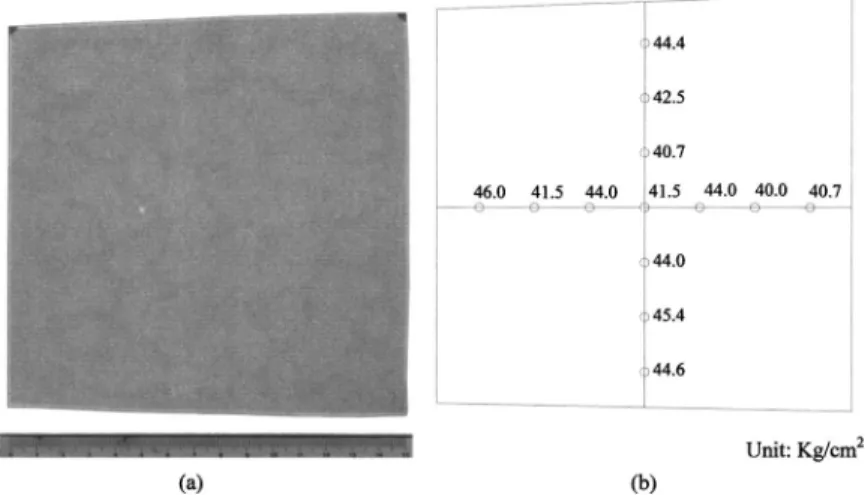
Pressure uniformity over a large area was investigated with pressure-sensitive films. The pressure sensitive film 共Fuji Prescale Film, Japan兲 can indicate pressures by colors from 25 to 100 Kg/ cm2. The pressure-sensitive film 共15 ⫻15 cm2兲 was sandwiched between an 8 in. PDMS mold and silicon wafer under the gas pressure of 45 Kg/ cm2. Color density of the pressed film was measured by a densi-tometer detector and the result was shown in Fig. 3共a兲. The measured pressure values over the imprint area were 43± 3 Kg/ cm2, as shown in Fig. 3共b兲. This proves that the PDMS mold and gas pressure mechanism can achieve the close contact and uniform pressing demonstrated for one-step direct imprinting on a large area substrate.
B. 12 in. silicon wafer imprinted
The first time 12 in. silicon wafer fully one-step imprint-ing has been achieved usimprint-ing the proposed process is shown in Fig. 4共a兲. It also can be seen imprinting uniformity around the wafer for a given pattern, as shown in Fig. 4共b兲. The patterns were constructed with a pitch of 3.2m and a width
FIG. 1. Schematic of the gas pressurized apparatus and imprinting process for a 12 in. silicon wafer and a 2 in. curved substrate imprinted. #1, process for planar imprinting; #2, process for nonplanar imprinting
FIG. 2. Photograph of a 12 in. PDMS mold fabricated procedure:共a兲 4 in. silicon mold with a series of patterned squares as a master mold;共b兲 PC film hot embossing;共c兲 assembled PC films up to a 12 in. diameter; 共d兲 12 in. PDMS mold casting;共e兲 SEM images on surface of silicon mold, PC film, and PDMS mold.
1688 Chang et al.: Direct imprinting using soft mold and gas pressure 1688
of 1.6m. The SEM images show that pattern structures were almost identical and defect-free for all the fields. In addition, the atomic force microscope 共AFM兲 images are shown in Fig. 4共c兲. The line structures on the PDMS mold and resist surfaces with opposite patterns at the same posi-tion are illustrated, displaying the width of 1.6m, depth of 350 nm, and pitch of 3.2m. By using a mold made from
PDMS, owing to the low interfacial free energy
共22–24 dyn/cm兲, it can be easily released without damaging the resist;3the pattern distortion can be significantly reduced due to the similar coefficient of thermal expansion between mold and resist. This indicates a success of imprinting pro-cess. The patterns were successfully transferred by one im-printing step on the entire wafer surface. These results show that the presented technology with the PDMS and the pres-sure system is good enough to duplicate the patterns on a very large surface. Note that the linewidth of 1.6m on the master mold is not the smallest scale for the soft mold and
gas pressure mechanism imprinting. In fact, the resolution can be further scaled below 1.6m by our fabricated process.
C. Nonplanar substrate imprinted
Figure 5共a兲 shows a photograph of a 2 in. curved substrate with a 3 in. radius of curvature imprinted using a gas pres-sure mechanism and a PDMS mold. Figure 5共b兲 shows the imprinted patterns on the curved surface. An optical micro-scope共OM兲 generated by a focusing microscope on the part of the sloping surface that lies in the center of the field of view. This image highlights the limited depth of field asso-ciated with conventional photolithographic methods. Due to the PDMS mold’s elastomeric character, the PDMS mold conforms its shape to the substrate surface, thus generating the smooth contact. These patterns were successfully repro-duced with a good shape pattern.
FIG. 3. 共a兲 Photograph of indicating papers 共15 ⫻15 cm2兲 under the gas pressure of 45 kg/cm2;共b兲 the
measured pressure values over the imprint area were 43± 3 kg/ cm2.
FIG. 4. 共a兲 Photograph of a 12 in. imprinted wafer; 共b兲 SEM images of three line patterns from a 12 in. silicon wafer, the minima feature size of 1.6m width; 共c兲 AFM images of a line with microstructures of 1.6m width and 3.2m pitch with 350 nm depth.
1689 Chang et al.: Direct imprinting using soft mold and gas pressure 1689
IV. CONCLUSIONS
From these results, the comparison of the traditional platen pressing and gas pressing with a soft mold process can be shown as Table I. It is confirmed that we can fabricate correctly patterns on a 12 in. silicon wafer and a 2 in. curved substrate in one imprint step without causing any defect us-ing a PDMS mold and gas pressure mechanism. Because the uniformity of the pressure was applied to perform imprinting in our fabricated process, the feature sizes of patterns were also consistent under the imprinting conditions.
V. SUMMARY
In this paper we present an innovative method and a mechanism for a very large area imprinting using gas pres-sure to press the soft mold and substrate. Replications of submicron features on a 12 in. silicon wafer and a 2 in. curved substrate in one step were demonstrated. SEM and AFM observations show uniform and clear transferred pat-terns into the PMMA resist. The high fidelity of feature rep-lication implies that the new process has its potential as a low-cost one-step direct large area imprinting for enhanced productivity.
ACKNOWLEDGMENTS
This work was supported by the National Science Council under Contract No. NSC 93-2218-E-002-017. Partial finan-cial support was also granted by the MLI Company. Spefinan-cial thanks to the Formosa Komatsu Silicon Corporation for the 12 in. silicon wafer supply were appreciated. We also thank Professor Lo for carrying out the AFM measure and co-workers in the Grace Laboratory for providing experimental assistance for polymer processing.
1S. Y. Chou, P. R. Krauss, and P. J. Renstrom, Appl. Phys. Lett. 67, 3114
共1995兲.
2S. Y. Chou, P. R. Krauss, W. Zhang, L. Guo, and L. Zhuang, J. Vac. Sci.
Technol. A 15, 2897共1997兲.
3J. L. Wilbur, A. Kumar, E. Kim, and G. M. Whitesides, Adv. Mater.
共Weinheim, Ger.兲 6, 601 共1994兲.
4Y. Xia and G. M. Whitesides, Annu. Rev. Mater. Sci. 28, 153共1998兲. 5B. Vratzov, A. Fuchs, M. Lemme, W. Henschel, and H. Kurz, J. Vac. Sci.
Technol. B 21, 2760共2003兲.
6U. Plachetka, M. Bender, A. Fuchs, M. Otto, B. Vratzov, B. Vratzov,
T. Gilnsner, F. Lindner, and H. Kurz, Microelectron. Eng. 73–74, 167 共2004兲.
7T. Bailey, B. Smith, B. J. Choi, M. Colburn, M. Meissl, S. V. Sreenivasan,
J. G. Ekerdt, and C. G. Willsona, J. Vac. Sci. Technol. B 19, 2806共2001兲.
8T. Bailey, B. J. Choi, M. Meissl, S. Shaya, J. G. Ekerdt, S. V. Sreenivasan,
and C. G. Willson, J. Vac. Sci. Technol. B 18, 3572共2000兲.
9C. Gourgon, C. Perret, J. Tallal, F. Lazzarino, S. Landis, O. Joubert, and
R. Pelzer, J. Phys. D 38, 70共2005兲.
10J. H. Chang and S. Y. Yang, Microsyst. Technol. 10, 76共2003兲. 11H. Tan, L. Kong, M. Li, C. Steere, and L. Koecher, SPIE’s The
Interna-tional Society for Optical Engineering: Emerging Lithographic Technolo-gies VIII, 2004, pp. 213–221.
12P. Ruchhoeft, M. Colburn, B. Choi, H. Nounu, S. Johnson, T. Bailey,
S. Damle, M. Stewart, J. G. Ekerdt, S. V. Sreenivasan, J. C. Wolfe, and C. G. Willson, J. Vac. Sci. Technol. B 17, 2965共1999兲.
13K. E. Paul, M. Prentiss, and G. M. Whitesides, Adv. Funct. Mater. 13,
259共2003兲.
14W. M. Choi and O. O. Park, Nanotechnology 15, 1767共2004兲.
FIG. 5. Nonplanar surface imprinted:共a兲 photograph of a 2 in. curved stain-less steel with a 3 in. radius of curvature;共b兲 OM images of patterns of line and triangular on a curved surface.
TABLEI. A comparison of the traditional platen pressing and gas pressing with soft mold process.
Platen pressing
Gas pressing with soft mold Pressure distribution Nonuniform Excellent uniform
Imprinting area Small Very large
Tool material Hard Hard/Soft
Substrate shape Planar Planar/Curve
UV exposure Difficulty Easy
Cost High Low
1690 Chang et al.: Direct imprinting using soft mold and gas pressure 1690