characteristic is practically without variation. Gain of 8 dBi and VSWR of less than 2 at 220-MHz frequency have been obtained. The concept of the presented antenna array may be used for frequencies from some hundreds of MHz to about 30 GHz. ACKNOWLEDGMENTS
The authors are grateful to Ivana Radnovic, Milka Marjanovic, Momcilo Tasic, Zoran Micic, and Milica Rakic for their help with realization and measurement. This work was supported by the Serbian Ministry for Science, Technologies, and Development. REFERENCES
1. K.-L. Wong, J.-W. Lai, and F.-R. Hsiao, Omnidirectional planar dipole-array antenna for 2.4/5.2-GHz WLAN access points, Microwave Opt Technol Lett 39 (2003), 33–36.
2. K.L. Wong, Planar antennas for wireless communication, Wiley, New York, 2003, p. 219.
3. M. Mikavica and A. Nesic, A, CAD for linear and planar antenna array of various radiating elements, Artech House, Norwood, MA, 1992. 4. H. Miyashita, H. Ohmine, K. Nishizawa, S. Makino, and S. Urasaki,
Electromagnetically coupled coaxial dipole array antenna, IEEE Trans Antenna Propagat 47 (1999), 1716 –1725.
5. A.D. Djordjevic, M.B. Bazdar, R.F. Harrington, and T.K. Sarkar, LIN-PAR, for Windows: Matrix parameters for multiconductor transmission lines, Software and user’s manual, Version 1.0, Artech House, Nor-wood, MA, 1999.
6. IE3D, Zeland Software, Inc., Fremont, CA 4538, version 4.0. © 2004 Wiley Periodicals, Inc. AQ1 Is “Zc” OK as is or make italic?
DC–12-GHz 10-dB GAIN SHUNT-SERIES
SHUNT-SHUNT WIDEBAND AMPLIFIERS
BY COMMERCIALLY AVAILABLE 0.35
M SiGe HBT TECHNOLOGY
C. C. Meng,1T. H. Wu,1and G. W. Huang2 1Department of Communication Engineering
National Chiao Tung University Hsinchu, Taiwan, R.O.C.
2National Nano Device Laboratories
Hsinchu, Taiwan, R.O.C.
Received 28 August 2003
ABSTRACT: The realization of wideband amplifiers with shunt-series
shunt-shunt dual-feedback configuration with commercially available 0.35-m SiGe BiCMOS technology is reported. The SiGe HBT used here has ftof 67 GHz and BVceo of 2.5 V. The experimental results
show that power gain is 10 dB from DC to 12 GHz for a shunt-series shunt-shunt wideband amplifier, with the help of the emitter capacitive peaking technique. Input- and output-return losses are better than 10 dB for the same frequency range. Noise figure increases from 8 to 12 dB for frequencies from 1 to 18 GHz. OP1dBand OIP3are 0 dBm and 12
dBm at 1 GHz, respectively. Total current consumption is 11 mA at 3.3 V supply voltage. © 2004 Wiley Periodicals, Inc. Microwave Opt
Technol Lett 40: 518 –520, 2004; Published online in Wiley InterScience (www.interscience.wiley.com). DOI 10.1002/mop.20021
Key words: SiGe; HBT; amplifiers INTRODUCTION
Wideband amplifiers [1– 4] are used in a variety of modern com-munication systems. The Kukielka wideband amplifier is one of the most popular circuit topologies among all kinds of wideband amplifiers. The matched-impedance Kukielka wideband amplifier
is achieved by using a shunt-series shunt-shunt dual-feedback configuration. In this work, SiGe HBT Kukielka wideband ampli-fiers are demonstrated by a commercially available foundry ser-vice. The 0.35-m SiGe BiCMOS process is very economical because it is fabricated using the inexpensive I-line photolithog-raphy technique instead of the expensive deep-UV technique, and even the phase-shift mask photolithography technique is used for feature length of 0.25m and below.
The circuit schematic of the designed shunt-series shunt-shunt SiGe HBT wideband amplifier is shown in Figure 1. A Darlington pair is used in the second stage to improve the frequency response. The resistors Rf 1and Rf 2in Figure 1 are the global feedback and
local feedback resistors, respectively. The resistor Rf 1is shunting at input and Rf 2is shunting at output, in order to lower the terminal
impedance to 50⍀ for the terminal impedance matching. The emitter peaking capacitors Ce1and Ce2are shown in Figure 1. The
emitter capacitive peaking technique is used to overcome the Figure 1 Circuit schematic of the shunt-series shunt-shunt SiGe HBT wideband amplifier
Figure 2 Die photo of the shunt-series shunt-shunt dual feedback SiGe HBT wideband amplifier
intrinsic over-damped frequency response of the shunt-series shunt-shunt wideband amplifier and thus enhance the bandwidth [2, 5, 6]. The design principles of gain, bandwidth, and input/ output return loss have been well established [5] for the shunt-series shunt-shunt wideband amplifier. Thus, 10-dB gain and in-put/output return loss of better than 10 dB are designed and demonstrated from DC to 12 GHz in this work.
MEASUREMENT RESULTS
Figure 2 illustrates the die photo of the fabricated SiGe HBT dual-feedback amplifier. The SiGe HBT device used here has ftof 67 GHz
and BVceo of 2.5 V. The amplifier has a coplanar ground-signal-ground pad to facilitate on-wafer probing. The size of all the SiGe HBT transistors in Figure 2 is 0.3⫻ 9.9m. The small emitter width reduces the intrinsic base resistance and intrinsic base-collector junc-tion capacitor for higher fmax. The die size is 0.7⫻ 0.7 mm. Most of
the die area is not fully utilized to facilitate the on-wafer measurement and the die size of the wideband feedback amplifier can be easily compacted into 0.4⫻ 0.4 mm.
The first stage consumes 3 mA and the second stage consumes 8 mA at 3.3-V supply voltage. Figure 3 shows the forward trans-mission gain, input-return loss, reverse transtrans-mission gain, and output-return loss for 3.3-V supply voltage. The shunt-series shunt-shunt dual feedback. SiGe wideband amplifier has 12 GHz of 3-dB gain bandwidth, S11 and S22are below⫺10 dB for the measurement range from DC to 18 GHz, as illustrated in Figure 3 for 3.3-V supply voltage.
The rf performance of the same SiGe wideband amplifier at 2.5-V supply voltage is also illustrated in Figure 4. The total bias current is 5 mA at 2.5-V supply voltage. The gain and bandwidth have been reduced to 8 dB and 8 GHz, respectively, as illustrated in Figure 4. Both bias conditions show that the terminal impedance matching is very good and the matching bandwidth is even higher than the 3-dB gain bandwidth.
Figures 5 and 6 illustrate the noise and power performances at both bias conditions. Noise performance is about one-half to one dB better at 3.3-V supply voltage. Noise figure increases from 8 to 12 dB for frequencies from 1 to 18 GHz at 3.3-V supply voltage. OP1dBand OIP3 of the wideband amplifier, operating at 3.3-V supply voltage as a function of frequency, are illustrated in Figure 7. OP1dBand OIP3are 0 and 12 dBm at 1 GHz, respectively. Both OP1dBand OIP3 decrease when the frequency becomes higher.
OP1dBand OIP3become⫺9 and 3 dBm at 12 GHz, respectively. OIP3is about 12-dB higher than OP1dBfor the measured frequency
range. CONCLUSION
This work has demonstrated a 10-dB gain DC–12-GHz SiGe HBT shunt-series shunt-shunt feedback wideband amplifiers by using a commercially available 0.35-m SiGe BiCMOS foundry. The total current consumption is 11 mA at 3.3-V supply voltage. The experimental results show that power gain is 10 dB and input/ output return loss is below 10 dB from DC to 12 GHz for the wideband amplifier at 3.3-V supply voltage. Noise figure increases from 8 to 12 dB for frequencies from 1 to 18 GHz. Both OP1dBand Figure 3 Measurement results of the SiGe HBT wideband amplifier with
Vcc ⫽ 3.3 V and Itotal⫽ 11 mA
Figure 4 Measurement results of the SiGe HBT wideband amplifier with
Vcc ⫽ 2.5 V and Itotal⫽ 5 mA
Figure 5 Measured noise figures of the SiGe HBT wideband amplifier
Figure 6 Measured power performance of the SiGe HBT wideband amplifier at 3.3-V supply voltage
OIP3 are a function of frequency. OP1dBand OIP3are 0 and 12 dBm at 1 GHz, respectively. Both OP1dBand OIP3decrease when frequency becomes higher. OP1dBand OIP3 become⫺9 and 3 dBm at 12 GHz, respectively.
ACKNOWLEDGMENTS
This work was supported by the National Science Council of Republic of China under grant no. NSC 92-2219-E-009-023 and by the Ministry of Education under grant no. 89-E-FA06-2-4. The authors also would like to thank the Chip Implementation Center in Taiwan for providing chip fabrication.
REFERENCES
1. R.G. Meyer and R.A. Blauschild, A 4-terminal wide-band monolithic amplifier, IEEE J Solid-State Circ SC-16 (1981), 634 – 638.
2. C.D. Hull and R.G. Meyer, Principles of monolithic wideband feedback amplifier design, Int J High-Speed Electron 3 (1992), 53–93. 3. K.W. Kobayashi and A.K. Oki, A DC-10 GHz high gain-low noise
GaAs HBT direct-coupled amplifier, IEEE Microwave Guided Wave Lett 5 (1995), 308 –310.
4. K.W. Kobayashi and A.K. Oki, A Low-noise baseband 5-GHz direct-coupled HBT amplifier with common-base active input match, IEEE Microwave Guided Wave Lett 4 (1994), 373–375.
5. M.C. Chiang, S.S. Lu, C.C. Meng, S.A. Yu, S.C. Yang, and Y.J. Chan, Analysis, design, and optimization of InGaP-GaAs HBT matched-impedance wide-band amplifiers with multiple feedback loops, IEEE J Solid-State Circ 37 (2002), 694 –701.
6. C.C. Meng, T.H. Wu, and S.S. Lu, 28-dB Gain DC-6GHz GaInP/GaAs HBT Wideband Amplifiers with and without Emitter Capacitive Peak-ing, Euro Gallium Arsenide and other Semiconductors Appl Symp (GAAS 2002), 2002, pp. 311–314.
© 2004 Wiley Periodicals, Inc.
AN ENHANCED CAVITY MODEL FOR
MICROSTRIP ANTENNAS
Yeow-Beng Gan,1Chee-Parng Chua,2and Le-Wei Li2,3 1Tamasek Laboratories
Singapore 119260
2Dept. of Electrical Computer Engineering
National University of Singapore 10 Kent Ridge Crescent Singapore 119260
3HPCES Program
Singapore-MIT Alliance Singapore 119260
Received 21 August 2003
ABSTRACT: An enhanced cavity model for analyzing microstrip patch
antenna is presented. The predicted resonant frequency and resonant resistance of the antenna are in good agreement with measured data. Theoretical results of the enhanced model are also compared with some commonly used models to determine their range of validity. © 2004
Wiley Periodicals, Inc. Microwave Opt Technol Lett 40: 520 –523, 2004; Published online in Wiley InterScience (www.interscience.wiley. com). DOI 10.1002/mop.20022
Key words: cavity model; microstrip antennas; antenna analysis 1. INTRODUCTION
A conventional microstrip antenna is usually comprised of a me-tallic patch deposited on one side of the substrate and a ground plane on the other side. Over the years, many models [1– 6] have
been used to analyze microstrip patch geometry. Among them, the cavity model with perfect magnetic conducting (PMC) walls has been useful in providing insight regarding the radiation mecha-nisms of microstrip patch, but has also provided inaccurate pre-diction of its resonant frequent and resonant resistance. In this model, the thickness t of the microstrip patch antenna’s substrate has been assumed to be electrically thin (usually on the order of 0.010) and a low dielectric constant has been used. These two
assumptions made by the analytical models no longer hold because the microstrip patch antenna is increasingly used in the millimeter-wave region. To achieve miniaturization and larger bandwidth, thicker and higher dielectric substrate is also commonly used. Hence, a better analytical model or technique is needed to char-acterize the microstrip patch antenna.
2. ENHANCED MODEL
The enhanced cavity model is based on Carver and Coffey’s [2, 3] design equations formulated for microstrip patch resonator using the modal-expansion technique. In this approach, the patch is viewed as a thin TMz-mode cavity supporting quasi-discrete
TMmnmodes transverse to z, where m and n are the mode numbers
associated with the x and y directions, respectively. The field between the patch and the ground plane is expanded in terms of a series of eigenfunctions with their corresponding eigenvalues. For a nonradiating cavity, these eigenvalues are positive and real and are defined as kx ⫽ n/a and ky ⫽ m/b. For the cavity to
radiate, the interior fields must be related to the exterior fields. This is achieved by imposing impedance boundary conditions at the four walls by making use of fictitious complex wall admittances Yw to represent the external stored and radiated energy effects.
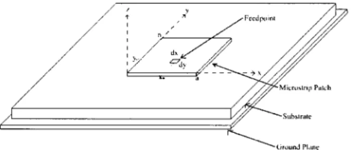
Consider a microstrip patch antenna (shown in Fig. 1) of resonant length b (⬇d/ 2) along the y direction and width a (⬇2b), the
following transcendental equation is obtained [3]:
tan共kyb兲 ⫽ 2ky␣y ky2⫺␣y2 , (1) where ␣y⫽ j 20 0 t aYwFy
冉
a b冊
, Fy⫽ 0.7747 ⫹ 0.5977冉
a b⫺ 1冊
⫺ 0.1638冉
a b⫺ 1冊
2 .The wall admittance Ywis multiplied by a factor Fyto take into
consideration the effect of the aspect ratio a/b on the accuracy of the mode vectors used to represent the actual field distribution at the radiating edges. Better agreement between the predicted and measured results was found in comparison to Fy⫽ 1. The wall
Figure 1 Rectangular microstrip patch antenna used in the experiment