Aperiodic and randomized dielectric mirrors:
alternatives to metallic back reflectors for solar
cells
Albert Lin,* Yan-Kai Zhong, Sze-Ming Fu, Chi Wei Tseng, and Sheng Lun Yan
Department of Electronic Engineering, National Chiao-Tung Univeristy, Hsinchu 30010, Taiwan
*hdtd5746@gmail.com
Abstract: Dielectric mirrors have recently emerged for solar cells due to the
advantages of lower cost, lower temperature processing, higher throughput, and zero plasmonic absorption as compared to conventional metallic counterparts. Nonetheless, in the past, efforts for incorporating dielectric mirrors into photovoltaics were not successful due to limited bandwidth and insufficient light scattering that prevented their wide usage. In this work, it is shown that the key for ultra-broadband dielectric mirrors is aperiodicity, or randomization. In addition, it has been proven that dielectric mirrors can be widely applicable to thin-film and thick wafer-based solar cells to provide for light trapping comparable to conventional metallic back reflectors at their respective optimal geometries. Finally, the near-field angular emission plot of Poynting vectors is conducted, and it further confirms the superior light-scattering property of dielectric mirrors, especially for diffuse medium reflectors, despite the absence of surface plasmon excitation. The preliminary experimental results also confirm the high feasibility of dielectric mirrors for photovoltaics.
©2014 Optical Society of America
OCIS codes: (310.6845) Thin film devices and applications; (040.5350) Photovoltaic;
(050.1940) Diffraction.
References and links
1. S. Hänni, G. Bugnon, G. Parascandolo, M. Boccard, J. Escarré, M. Despeisse, F. Meillaud, and C. Ballif, “High-efficiency microcrystalline silicon single-junction solar cells,” Prog. Photovolt. Res. Appl. 21, 821–826 (2013). 2. B. Lipovšek, J. Krč, O. Isabella, M. Zeman, and M. Topič, “Modeling and optimization of white paint back
reflectors for thin-film silicon solar cells,” J. Appl. Phys. 108(10), 103115 (2010).
3. P. Bermel, C. Luo, L. Zeng, L. C. Kimerling, and J. D. Joannopoulos, “Improving thin-film crystalline silicon solar cell efficiencies with photonic crystals,” Opt. Express 15(25), 16986–17000 (2007).
4. X. Sheng, S. G. Johnson, L. Z. Broderick, J. Michel, and L. C. Kimerling, “Integrated photonic structures for light trapping in thin-film Si solar cells,” Appl. Phys. Lett. 100(11), 111110 (2012).
5. S. L. Chuang, Physics of Photonic Devices, 2nd ed. (Wiley, 2009).
6. P. Bhattacharya, Semiconductor Optoelectronic Devices, 2nd ed. (Prentice-Hall, 2006).
7. J. D. Joannopoulos, S. G. Johnson, R. D. Meade, and J. N. Winn, Photonic Crystal: Molding the Flow of Light, 2 ed. (Princeton University Press, 2008).
8. Y.-C. Lee, C.-F. Huang, J.-Y. Chang, and M.-L. Wu, “Enhanced light trapping based on guided mode resonance effect for thin-film silicon solar cells with two filling-factor gratings,” Opt. Express 16(11), 7969–7975 (2008). 9. L. Dal Negro, C. Oton, Z. Gaburro, L. Pavesi, P. Johnson, A. Lagendijk, R. Righini, M. Colocci, and D.
Wiersma, “Light transport through the band-edge states of Fibonacci quasicrystals,” Phys. Rev. Lett. 90(5), 055501 (2003).
10. W. Gellermann, M. Kohmoto, B. Sutherland, and P. C. Taylor, “Localization of light waves in Fibonacci dielectric multilayers,” Phys. Rev. Lett. 72(5), 633–636 (1994).
11. L. Dal Negro, M. Stolfi, Y. Yi, J. Michel, X. Duan, L. C. Kimerling, J. LeBlanc, and J. Haavisto, “Photon band gap properties and omnidirectional reflectance in Si/SiO 2 Thue–Morse quasicrystals,” Appl. Phys. Lett. 84(25), 5186 (2004).
12. C. Lin, N. Huang, and M. L. Povinelli, “Effect of aperiodicity on the broadband reflection of silicon nanorod structures for photovoltaics,” Opt. Express 20(1 S1), A125–A132 (2012).
13. C. Lin and M. L. Povinelli, “Optimal design of aperiodic, vertical silicon nanowire structures for photovoltaics,” Opt. Express 19(Suppl 5), A1148–A1154 (2011).
15. A. Oskooi, P. A. Favuzzi, Y. Tanaka, H. Shigeta, Y. Kawakami, and S. Noda, “Partially disordered photonic-crystal thin films for enhanced and robust photovoltaics,” Appl. Phys. Lett. 100(18), 181110 (2012). 16. K. Vynck, M. Burresi, F. Riboli, and D. S. Wiersma, “Photon management in two-dimensional disordered
media,” Nat. Mater. 11(12), 1017–1022 (2012).
17. F. Pratesi, M. Burresi, F. Riboli, K. Vynck, and D. S. Wiersma, “Disordered photonic structures for light harvesting in solar cells,” Opt. Express 21(Suppl 3), A460–A468 (2013).
18. A. Bozzola, M. Liscidini, and L. C. Andreani, “Broadband light trapping with disordered photonic structures in thin-film silicon solar cells,” Prog. Photovolt. Res. Appl. 21, 2385 (2013).
19. E. R. Martins, J. Li, Y. Liu, V. Depauw, Z. Chen, J. Zhou, and T. F. Krauss, “Deterministic quasi-random nanostructures for photon control,” Nat. Commun. 4, 2665 (2013).
20. M. Burresi, F. Pratesi, K. Vynck, M. Prasciolu, M. Tormen, and D. S. Wiersma, “Two-dimensional disorder for broadband, omnidirectional and polarization-insensitive absorption,” Opt. Express 21(Suppl 2), A268–A275 (2013).
21. P. Spinelli, M. A. Verschuuren, and A. Polman, “Broadband omnidirectional antireflection coating based on subwavelength surface Mie resonators,” Nat. Commun. 3, 692 (2012).
22. P. Nitz, J. Ferber, R. Stangl, H. R. Wilson, and V. Wittwer, “Simulation of multiply scattering media,” Sol. Energ. Mat. Sol. Cells 54(1-4), 297–307 (1998).
23. W. E. Vargas, A. Amador, and G. A. Niklasson, “Diffuse reflectance of TiO2 pigmented paints: spectral
dependence of the average path length parameter and the forward scattering ratio,” Opt. Commun. 261(1), 71–78 (2006).
24. W. E. Vargas, P. Greenwood, J. E. Otterstedt, and G. A. Niklasson, “Light scattering in pigmented coatings: experiment and theory,” Sol. Energy 68(6), 553–561 (2000).
25. J. E. Cotter, “Optical intensity of light in layers of silicon with rear diffuse reflectors,” J. Appl. Phys. 84(1), 618– 624 (1998).
26. S. Preble, M. Lipson, and H. Lipson, “Two-dimensional photonic crystals designed by evolutionary algorithms,” Appl. Phys. Lett. 86, 061111 (2005).
27. B. Deken, S. Pekarek, and F. Dogan, “Minimization of field enhancement in multilayer capacitors,” Comput. Mater. Sci. 37(3), 401–409 (2006).
28. J. B. Pollack and H. Lipson, “Automatic design and manufacture of robotic life forms,” Nature 406(6799), 974– 978 (2000).
29. L. Shen, Z. Ye, and S. He, “Design of two-dimensional photonic crystals with large absolute band gaps using a genetic algorithm,” Phys. Rev. B 68, 035109 (2003).
30. Rsoft, Rsoft CAD User Manual, 8.2 ed. (Rsoft Design Group, 2010).
31. L. Miao, S. Tanemura, S. Toh, K. Kaneko, and M. Tanemura, “Preparation and characterization of rutile TiO2 nanorods,” J. Mater. Sci. Technol. 20, 59–62 (2004).
32. O. S. o. America, Handbook of Optics, 2nd ed. (McGraw-Hill Professional, 1994), Vol. 2.
33. E. D. Palik, Handbook of Optical Constants of Solids (Academic Press Handbook Series, 1985). 34. J. R. Devore, “Refractive indices of rutile and sphalerite,” J. Opt. Soc. Am. 41(6), 416–419 (1951).
35. C. Battaglia, C.-M. Hsu, K. Söderström, J. Escarré, F.-J. Haug, M. Charrière, M. Boccard, M. Despeisse, D. T. L. Alexander, M. Cantoni, Y. Cui, and C. Ballif, “Light trapping in solar cells: can periodic beat random?” ACS Nano 6(3), 2790–2797 (2012).
36. K. Söderström, F.-J. Haug, J. Escarré, O. Cubero, and C. Ballif, “Photocurrent increase in n-i-p thin film silicon solar cells by guided mode excitation via grating coupler,” Appl. Phys. Lett. 96(21), 213508 (2010).
37. O. Deparis and O. El Daif, “Optimization of slow light one-dimensional Bragg structures for photocurrent enhancement in solar cells,” Opt. Lett. 37(20), 4230–4232 (2012).
38. A. Lin, Y.-K. Zhong, and S.-M. Fu, “The effect of mode excitations on the absorption enhancement for silicon thin film solar cells,” J. Appl. Phys. 114(23), 233104 (2013).
39. H.-Y. Lin, Y. Kuo, C.-Y. Liao, C. C. Yang, and Y.-W. Kiang, “Surface plasmon effects in the absorption enhancements of amorphous silicon solar cells with periodical metal nanowall and nanopillar structures,” Opt. Express 20(1 S1), A104–A118 (2012).
40. S. Pillai, F. J. Beck, K. R. Catchpole, Z. Ouyang, and M. A. Green, “The effect of dielectric spacer thickness on surface plasmon enhanced solar cells for front and rear side depositions,” J. Appl. Phys. 109(7), 073105 (2011). 41. U. W. Paetzold, E. Moulin, B. E. Pieters, R. Carius, and U. Rau, “Design of nanostructured plasmonic back
contacts for thin-film silicon solar cells,” Opt. Express 19(Suppl 6), A1219–A1230 (2011).
42. U. W. Paetzold, E. Moulin, D. Michaelis, W. Bottler, C. Wächter, V. Hagemann, M. Meier, R. Carius, and U. Rau, “Plasmonic reflection grating back contacts for microcrystalline silicon solar cells,” Appl. Phys. Lett.
99(18), 181105 (2011). 1. Introduction
Dielectric mirrors have the benefits of lower cost, lower temperature processing, high throughput, and zero plasmonic loss [1,2]. This is easiest to understand when diffuse medium reflectors are used as an example [1,2]. The problem with previous designs of dielectric reflectors for solar cells is primarily limited bandwidth [3,4] and in some cases insufficient light scattering due to the absence of surface plasmon emission. Conventional distributed Bragg reflectors (DBR) generally do not provide a wide enough reflection bandwidth for
photovoltaic applications [5–7]. If the target wavelength of 400–1000 nm is selected, the
bandwidth for a DBR is around 300 nm for silicon dioxide/titanium oxide (SiO2/TiO2)
systems. For a leaky-mode-based grating mirror or an equivalently high-index contrast mirror (HCG), the reflection bandwidth is still insufficient for solar cells. For target wavelengths from 400–1000 nm, the reflection bandwidth for an HCG is around 200 nm for silicon dioxide/silicon (SiO2/Si) systems. In addition, integration of this type of dielectric mirror into
solar cells will lead to a situation where removing the active absorption materials becomes necessary [8]. Besides, selection of a wide-bandgap material with a refractive index greater than 3 to form an HCG is quite difficult since the refractive indices of most wide-bandgap semiconductors are smaller than 3.
Earlier work has been conducted to investigate aperiodic structures [9–12] in nanophotonics. There are also some pioneering works exploring the possibility of using aperiodicity for solar cells [13–19], including the supercell concept and quasi-random structures [14,19], aperiodic nanowires [13], and disordered media [15,16,18,20].
In this paper, we show that the key to achieving ultra-broadband high reflectance for dielectric mirrors is through randomness and aperiodicity, and this is the key to constructing all-dielectric solar cells. In addition to reflectance, the integrated absorbance weighted by the solar AM1.5 spectrum is also an important indication for the quality of solar cell back reflectors. In order to compare the light trapping of various metallic and dielectric mirrors, different solar cell structures with dielectric or metallic reflectors are compared side by side, with the geometry systematically optimized by genetic algorithms. For dielectric mirrors, an aperiodic DBR (A-DBR) and diffuse medium reflectors are used as examples. For metallic mirrors, different structures with or without dielectric spacers are studied, and the selection of the proper metallic mirror configuration for maximized absorbance will be discussed. It will be shown that the light trapping provided by diffuse medium reflectors or A-DBRs is actually comparable to conventional metallic back reflectors. The long-wavelength light scattering properties for dielectric mirrors are further studied by examining the polar plots of near-field time-averaged Poynting vectors to clarify the achievable emission angle in the absence of surface plasmon excitation. It will be shown later in this work that aperiodic or randomized dielectric mirrors are actually more promising than metallic mirrors for either thick wafer-based solar cells or thin-film devices. This is due to the fact that while the light trapping provided by dielectric mirrors can be comparable to metallic ones, the dielectric mirrors such as diffuse medium reflectors have the additional advantages of lower cost, lower temperature processing, and higher throughput [1,2].
2. Problem setup and algorithm-optimized geometry
hg
Λ
FF
Λ
SiO2 Si Anti-Reflection Coatingt
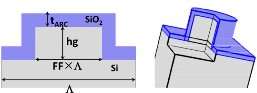
ARCFig. 1. Illustration of the solar cell stack in this study and the front surface structure. The Mie resonator-based design [21], or equivalent photonic-crystal circular grating arranged in a square lattice, is selected to be the solar cell front surface nanostructure.
The front surface nanostructure for all of the solar cell stacks in this study is uniformly selected as the Mie resonator-based design to facilitate a fair side-by-side comparison between dielectric and metallic mirrors [21] as illustrated in Fig. 1.
The first solar cell structure under study is an A-DBR-based design with a silicon absorber and anti-reflection coating (ARC) realized by Mie dielectric resonators [21]. The titanium oxide (TiO2)/silicon dioxide is used for alternating layers. If the thickness of the absorber is
thick enough, e.g., >500 nm for silicon, light trapping is generally not necessary for a wavelength below 600 nm. This means the reflection band of back reflectors can start from λ=600 nm instead of λ=400 nm. In the case in which only the long-wavelength portion of the solar spectrum, i.e., λ>600 nm, requires solar cell light trapping, other dielectric materials such as silicon nitride (Si3N4), indium tin oxide (ITO), or aluminum-doped zinc oxide (AZO)
can be used instead. Nonetheless, it is worth mentioning that, for other applications such as triple-junction cells or intermediate-band solar cells, ultra-wideband design becomes essential since the wide absorption spectrum results from the joint effect of the sub-cells or from the addition of intermediate states. As a result, the reflection mirror in this case should cover a very wide spectral range. Previous designs using a periodic DBR generally resulted in limited bandwidth [3,4], which does not cover the entire solar spectrum of interest for silicon photovoltaics. Here, an aperiodically designed DBR is shown to be capable of providing bandwidth covering the entire portion of the solar spectrum of interest for silicon materials.
The second structure under investigation is one of white paint back reflector-based solar
cells [1,2]. The white paint reflector generally consists of TiO2 or other dielectric
nanoparticles embedded in low-index polymer-based or oxide-based host materials. It falls into the category of diffuse medium reflectors. The white paint reflector is very promising for photovoltaics because of its lower cost, lower temperature processing, higher throughput, and zero plasmonic absorption loss [1,2]. Analysis along the line of the Monte Carlo method [22], N-flux methods based on radiation transfer equations [23–25], and one-dimensional (1D) approximation based on semi-coherent optical modeling [2] have been conducted for diffuse medium reflectors, but the wave optics analysis especially for solar cell structures has not been thoroughly investigated. In this work, the light trapping of diffuse medium reflectors and comparison to metallic mirrors will be carefully examined.
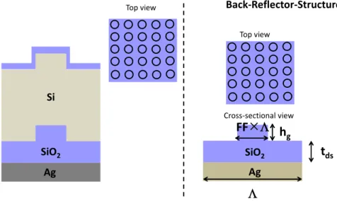
For metallic back reflectors, several different back reflector structures are possible, including dielectric-spaced metallic reflectors or metallic reflectors directly in contact with semiconductors. In this work, the optimal metallic reflector configuration is chosen, and geometry optimization is conducted to maximize the integrated absorbance. The result is then compared to dielectric mirror-backed solar cells. Angular emission plots for time-averaged Poynting vectors are then examined to compare the light scattering behavior for the metallic and dielectric mirrors.
A genetic algorithm is chosen as a global optimization algorithm due to its success in different fields of science and engineering [26–29] and the advantage that it does not require initial guesses. The material parameters are from the Rsoft material database [30] and literature [31–34]. Crystalline silicon parameters are used for both thick and thin absorber case studies due to the fact that the majority of the current photovoltaic market is still for wafer-based crystalline silicon or multi-crystalline silicon solar cells. Although crystalline silicon is used as an example, other inorganic semiconductors such as polycrystalline or amorphous silicon, gallium arsenide (GaAs), or cadmium telluride (CdTe) can also be used to demonstrate the effectiveness of the dielectric mirrors in this study. The result will be the same due to similar light trapping behaviors in inorganic solar cells. The calculation method is based on rigorously coupled wave analysis (RCWA) implemented by Rsoft Diffractmode. The polarization angle is 45°, and therefore the result is the average of s- and p-polarization.
{
*}
2 0 1 ( ) 2 A( ) , 1 Re ( ( ) ) ( ) 2 V S E r dv E r H r ds ωε ε λ λ ′′ = × ⋅
(1)where ω is the angular frequency, λ is the free-space wavelength, ε0 is the permittivity in
vacuum, and ε″ is the imaginary part of a complex semiconductor dielectric constant. The
integrated absorbance weighted by the AM 1.5 spectrum can be defined as:
Int ( )A( ) A , ( ) d hc d hc λ λ λ λ λ λ λ Ω = Ω
(2)where Ω(λ) is the AM 1.5 solar spectrum in unit # s−1 nm−1 m−2, h is the Plank constant, λ is
the free-space wavelength, and c is the speed of light. Since the AM 1.5 solar spectrum is in the number of photons, it is actually exactly the same as the photocurrent, assuming perfect charge collection.
3. DBR-based design using optimized aperiodicity
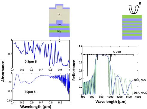
The first structure under study is illustrated in Fig. 2. The solar cell stacks consist of an ARC illustrated in Fig. 1, a silicon absorber, and the A-DBR illustrated in Fig. 2. For a periodic DBR, the high reflection is due to the constructive phase interference between reflected waves by the quarter wave slabs. Nonetheless, interference-based high reflectance is very difficult to achieve in ultra-broadband. This is due to the fact that the condition for constructive interference can only be perfectly fulfilled at the target wavelength, and the reflectance will gradually degrade when the wavelength begins to deviate from the target one. On the other hand, high reflectance for the aperiodic design proposed here is due to random light scattering. In this scenario, the successive phase addition for reflected waves leads to high reflectance. Although reflectance at the target wavelength for the A-DBR may not be as high as for a periodic DBR, the bandwidth of the A-DBR can be significantly widened while maintaining a high enough reflectance, as evident in Fig. 3. The reason that the broadband reflection can exist for the aperiodic structure is due to the fact that radiation modes, i.e., leaky modes, can continuously exist over the spectrum. This point has been quite clear from the literature on photonic crystals [7,35,36]. The thickness of each layer in the A-DBR is optimized individually in this section. It is thus self-evident that aperiodicity is the key to achieving broadband reflection. Conventional periodic DBRs [3,4,7] can only provide limited bandwidth, and therefore they are more appropriate for laser or detector applications but not for solar cells. From the reflectance plot for the A-DBR at the right of Fig. 3, it can be seen that it covers the entire spectral range of interest, i.e. λ=400 nm to λ=1000 nm. Comparison is made between the periodic DBR and the A-DBR in Fig. 3, where it is observed that the reflection bandwidth for the periodic DBR is 350 nm while the bandwidth of the A-DBR is 780 nm.
Back-Reflector-Structure nHTiO2 nLSiO2 t1 t2 t3 t4 … nH nL t2N N pairs, 2N layers Si
. . .
SiO2 TiO2 Top viewFig. 2. Illustration of the solar cell structure with an A-DBR. Layer thickness of an A-DBR can be optimized individually. Randomly determined layer thickness is also possible, and it can still lead to high reflectance.
For the mirror reflectance calculation at the right of Fig. 3, N=100 is used for the A-DBR to achieve ultra-broadband high reflectance, and the reflectance for periodic DBRs is also shown for comparison. For the integrated absorbance calculation for the entire solar cell stack structure illustrated at the left of Fig. 2, N=10 is used instead for the A-DBR to reduce the number of required deposited layers. The A-DBR with N=10 will have degraded reflectance at certain wavelengths as compared to the A-DBR with N=100. Nonetheless, an A-DBR with N=10 is more practical for a cost-sensitive solar application. The optimized geometry for the
solar cell with the A-DBR is Λ=513 nm, FF=0.77, hg=82 nm, tARC=81 nm for the case of a
thin absorber (300 nm), and is Λ=332 nm, FF=0.5, hg=108 nm, tARC=99 nm for the case of a
thick absorber (30 μm). The integrated absorbance for the A-DBR is 0.563 for a thin absorber (300 nm) and 0.984 for a thick absorber (30 μm). If a quarter-wavelength-slab periodic DBR with N=10 and center wavelength at λ=800 nm is used instead, the integrated absorbance for the A-DBR is 0.525 for a thin absorber (300 nm) and 0.984 for a thick absorber (30 μm). The comparison between different back reflectors is listed in Table 1 in Section 5. The layer thickness for the aperiodic DBR varies between 10 nm and 300 nm, and the full list is not included here since it is an extended list. For geometry parameters, please refer to Fig. 1 and Fig. 2. Layer thickness can also be randomly selected without significantly degraded absorbance. This reflects the importance of randomness and aperiodicity in a photovoltaic design using dielectric mirrors. The fabrication complexity for an A-DBR is a drawback for solar cell application. In the next section diffuse medium mirrors will be investigated, and they can provide much simpler processing than an A-DBR.
4000 600 800 1000 1200 1400 1600 0.2 0.4 0.6 0.8 1 1.2 0.4 0.5 0.6 0.7 0.8 0.9 1 0.85 0.9 0.95 1 R Wavelength (μm) Wavelength (μm) Re fl ec ta n ce Ab so rb an ce A-DBR DBR, N=5 DBR, N=20 0.4 0.5 0.6 0.7 0.8 0.9 1 0 0.5 1 30μm Si 0.3μm Si Si . . . SiO2 TiO2
Fig. 3. (Left) Spectral absorbance of the solar cell with an A-DBR, N=10 for A-DBR. (Right) reflectance for regular periodic DBR and A-DBR, N=100 for A-DBR.
4. Diffuse mirror-based design using randomness
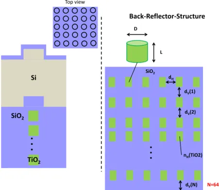
The second structure under study is a diffuse medium reflector that has recently shown to be very promising for solar cell application. The low-cost and low-temperature nature of diffuse medium reflectors can further decrease the cost for photovoltaics. The structure is an ARC illustrated in Fig. 1, a silicon absorber, and the white paint back reflectors illustrated in Fig. 4.
Common white paint reflectors generally consist of titanium oxide (TiO2) nanoparticles
embedded in a low-index host matrix material such as organic polymers or oxide-based dielectrics [2]. The superior light-scattering property of the embedded TiO2 is the key to high
reflectance and light trapping. The vertical spacing between TiO2 nanoparticles, dV, is
randomly varied here between 10 nm and 300 nm. In the horizontal direction, the TiO2
nanoparticles should also assume a random distribution in real diffuse medium reflectors. Nonetheless, if randomness in three dimensions is included, the computation is unmanageable. Therefore, a one-dimensional randomness approximation similar to [2], B. Lipovšek et al., is used here to capture the essential physics of diffuse medium reflectors. A
vertical spacing dV can also be optimized using a genetic algorithm, and the resulting
integrated absorbance value can be slightly higher. Since in real diffuse mirrors embedded
TiO2 nanoparticles with well-controlled spacing is more difficult to realize from the
fabrication point of view, the result for a randomly selected dV is included here. Based on our
study, either an aperiodically adjusted dV or a randomly varied dV leads to a broad reflection
band. As a result, it is obvious, from the study of diffuse medium reflectors and A-DBRs in the previous section, that the aperiodicity or randomness is the key for high-efficiency photovoltaics incorporating dielectric mirrors.
Si
. . .
SiO2 TiO2 Top view Back-Reflector-Structure SiO2 nH(TiO2) L D dH dV(1) dV(2). . .
dV(N) N=64Fig. 4. Illustration of the solar cell structure with white paint diffuse medium reflector. The TiO2 scatterers are cylindrical in shape to enhance the reflectance.
From the reflectance plot for the white paint back reflector, it can be seen that it covers the entire spectral range of interest, i.e., λ=400 nm to λ=1000 nm. In fact, the bandwidth that the diffuse medium reflector can achieve is even beyond 1000 nm, which is evident from the right side of Fig. 5. For spectral reflectance at the right of Fig. 5, dH=25 nm, D=229 nm, and L=71
nm to maximize the reflectance, and dV is randomly varied between 10 nm and 300 nm. For
the integrated absorbance calculation at the left of Fig. 5, AInt should be maximized, so the
optimized geometry will be slightly different from the one for the spectral reflectance. Nevertheless, the reflectance plot is insightful to show the superior reflection property of the diffuse medium reflector. In this work, the RCWA approach is used for the calculation. The high reflectance behavior associated with the diffuse medium reflector is confirmed by a finite-difference time domain (FDTD) method. The reflection peaks outside the reflection band are due to the coupling to the radiation modes, but with weaker coupling strength than the coupling within the reflection band. The reflectance dips in the spectral reflectance plot are due to the coupling into the Bloch propagation modes in the mirror structure [37]. Although it is not the main point in this paper, it is worth mentioning that a diffuse medium reflector has the advantage wherein the bandwidth can be widened by increasing the total number of the scattering sites in the wave propagation direction for a fixed-index contrast ratio. This can be done by increasing the thickness of the white paint reflector so that the photons encounter more scattering in the diffuse medium. This phenomenon is generally not possible for periodic structures, such as a periodic DBR where the index contrast pretty much determines the reflection bandwidth it can achieve. The optimized geometry for the solar cell
with white paint back reflectors is Λ=624 nm, tARC=97 nm, D=553 nm, L=277 nm, dH=70 nm,
FF=0.62, and hg=135 nm for the case of a thin absorber (300 nm), and is Λ=359 nm,
tARC=126 nm, D=244 nm, L=376 nm, dH=115 nm, FF=0.45, and hg=89 nm for the case of
thick absorber (30 μm). The vertical spacing dV is randomly varied between 10 nm and 300
nm. The number of TiO2 scatterers in the vertical direction is chosen to be N=64. For
with various back reflectors will be listed in Table 1 in Section 5. It should be pointed out that, unlike A-DBRs, the process of diffuse medium mirrors is very simple. The commercial white paint can actually be used, and room-temperature processing is easily achieved.
0.4 0.5 0.6 0.7 0.8 0.9 1 0 0.5 1 0.4 0.5 0.6 0.7 0.8 0.9 1 0.85 0.9 0.95 1 R . . . Wavelength (μm) Absorb an ce 30μm Si 0.3μm Si 0.5 1 1.5 0 0.2 0.4 0.6 0.8 1 1.2 Wavelength(μm) R efl ec ta n ce Si . . . SiO2 TiO2
Fig. 5. (Left) Spectral absorbance of the solar cell with a white paint diffuse medium reflector. (Right) Reflectance for the white paint diffuse medium reflector.
5. Metallic back reflector: the selection of the configurations
Ag
Ag
Ag
SiO
2Ag
SiO
2 (a) (b) (c) (d)Back-Reflector-Structure
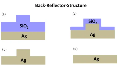
Fig. 6. Different configurations of metallic back reflectors for solar cells. (a) Planar metallic mirror with grating on the dielectric spacer. (b) Bare metallic mirror with grating. (c) Grated metallic mirror wrapped by a dielectric spacer. (d) Bare planar metallic mirror.
In order to compare dielectric mirrors and conventional metallic mirrors, spectral response and integrated absorbance solar cells with a metallic back reflector are investigated in this
reflector, illustrated in Fig. 7. Selection of the configuration for a metallic back reflector actually takes some consideration. Figure 6 illustrates several different metallic back reflector configurations with or without a dielectric spacer. From a fabrication point of view, for wafer-based crystalline silicon or multi-crystalline silicon solar cells, the configuration in Fig. 6(a) may have been more difficult to realize in the past, but with the rapid advances in silicon process technology, at present the difficulty can be easily overcome. For thin-film technology, all of the configurations in Fig. 6 can be realized easily, but the most common one in experimental thin-film solar cells is Fig. 6(c).
In the case of a bare metallic back reflector with grating in Fig. 6(b), metallic absorption generally outperforms surface plasmon emission [38]. For the planar metallic back reflector in Fig. 6(d), haze and light scattering are not sufficient. The planar metallic back reflector structure can be useful only if the ARC itself can provide a large enough scattering angle to ensure absorption enhancement in solar cells. There are two common dielectric-spaced metallic mirror structures. One is a metallic grating wrapped by a dielectric spacer, as shown in Fig. 6(c). The other one is the planar metallic mirror with grating on the dielectric spacer itself, as shown in Fig. 6(a). In fact, it has been shown that the planar metallic mirror with grating on the dielectric spacer in Fig. 6(a) is more appropriate for solar cell absorption enhancement [38]. This is due to the fact that plasmon absorption loss can be generally lower for the planar metal-dielectric interface. It will become clearer in the following section that although the metallic mirror in Fig. 6(c) can generally provide stronger field emission when compared to Fig. 6(a), plasmon absorption will outperform the consideration of the angular scattering. As a result, Fig. 6(a) is selected as the metallic back reflector for the absorbance calculation in Fig. 8 and Table 1.
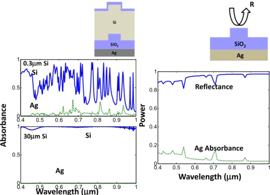
From the reflectance plot for metallic back reflectors in Fig. 8, it can be seen that although it covers the entire spectral range of interest, i.e. λ=400 nm to λ=1000 nm, significant plasmonic absorption also exists over the entire spectrum. Plasmon absorption will be enhanced even if grating is on the metal, such as in Fig. 6(c). The optimized geometry for the
solar cell with metallic back reflectors is Λ=539 nm, tARC=59 nm, FF=0.38, hg=194 nm, and
tds=187 nm for the case of a thin absorber (300 nm), and is Λ=400 nm, tARC=98 nm, FF=0.77,
hg=88 nm, and tds=82 nm for the case of a thick absorber (30 μm). For the geometry
parameters, please refer to Fig. 1 and Fig. 7. Table 1 compares the integrated absorbance weighted by the AM 1.5 spectrum for solar cells with various metallic and dielectric mirrors.
Ag SiO2
t
dsFF
Λ
Λ
h
g Top view Cross-sectional view SiO2 Ag SiTop view Back-Reflector-Structure
Fig. 7. Illustration of the solar cell structure with a metallic mirror. The selection of the metal back reflector configuration here is the best trade-off between plasmonic light scattering and metal absorption.
0.4 0.5 0.6 0.7 0.8 0.9 1 0 0.5 1 R
Wavelength (
μ
m)
Wavelength (
μ
m)
Po
w
er
Abs
o
rbanc
e
0.4 0.5 0.6 0.7 0.8 0.9 1 0 0.5 1 0.4 0.5 0.6 0.7 0.8 0.9 1 0 0.2 0.4 0.6 0.8 1 30μm Si 0.3μm Si Reflectance Ag Absorbance Ag Si Ag Si Ag SiO2 SiO2 Ag SiFig. 8. (Left) Spectral absorbance of the solar cell with a metallic mirror. (Right) Reflectance and metallic absorbance for the metallic mirror.
Table 1. Comparison of AM 1.5 Weighted Integrated Absorbance AInt
Mirror Type Periodic-DBR (300nm) A-DBR (300nm) WP Mirror (300nm) Metallic (300nm)
AInt 0.525 0.563 0.588 0.543
Mirror Type Periodic-DBR (30μm) A-DBR (30μm) WP Mirror (30μm) Metallic (30μm)
AInt 0.984 0.984 0.971 0.988
6. Angular emission for the dielectric and metallic back reflectors
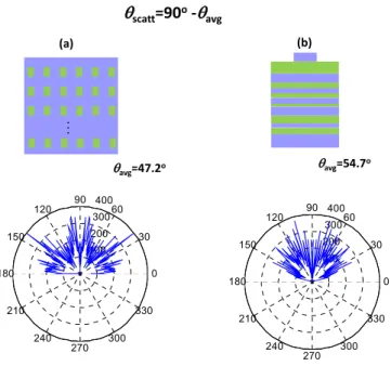
It is very interesting to examine the long-wavelength angular emission plots for various dielectric and metallic mirrors studied in this paper. Traditionally, the haze parameter is used to characterize the angular emission of solar cell back reflectors. In the nanophotonic regime, a haze parameter may not accurately describe the -rapping property for solar cells. As a result, the near-field field emission plot is constructed by plotting the time-averaged Poynting vector in a polar coordinate:
poynting, avg poynting, avg, x poynting, avg
* * , y Re{ ( ) ( )} 1Re{ ( ) ( 2 . 2 )} 1 z y x z P P P E r H r E r H r = + ∗ − ∗ = (3)
It is also possible to calculate the angular emission at the far field. In fact, the conclusion for comparison of different metallic and dielectric mirrors will not change if the far-field
advantage that it includes the in-plane propagation evanescent modes. This point is easiest to conceive by examining the formulation for eigenmode expansion:
z n m m z n, m n n, m n n m 2 2 2 z 0 m m n
exp( ) exp( ) exp( )
exp( ) e ( , , ) 2 2 xp( ) exp( ), 2 2 , E x y z n m a jk z jk x jk y a j y n m k z j x j k k π π π π = = − = Λ Λ Λ − Λ
(4)where k0 is the free space wave vector, Λn nad Λm is the period in the x and y directionz, n and
m are the expansion running index, and kz is the wave vector in the z direction (perpendicular
to the substrate). When it goes to higher-order modes, i.e., larger n and m, kz can become an
imaginary number, which corresponds to evanescent modes. For far-field angular plots, these modes will not be reflected. Nonetheless, it should be emphasized that the conclusion about the comparison between different mirrors will be the same; no matter near-field or far-field angular plots are constructed for comparison.
200 400 600 800 30 210 60 240 90 270 120 300 150 330 180 0 500 1000 30 210 60 240 90 270 120 300 150 330 180 0 Ag Ag SiO2 Ag SiO2 θavg=63.5o θavg=57.5 o θavg=50.8o
θ
scatt=90o-θ
avg (a) (b) (c) 200 400 600 30 210 60 240 90 270 120 300 150 330 180 0Fig. 9. Long-wavelength angular emission plot at λ=1 μm for metallic mirrors. (a) Planar metallic mirror with grating on the dielectric spacer. (b) Metallic grating mirror wrapped by a dielectric spacer. (c) Bare metallic mirror with grating. Larger θscatt, or equivalently smaller θavg,
θavg=47.2o θavg=54.7 o . . . θscatt=90o-θavg (a) (b) 100 200 300 400 30 210 60 240 90 270 120 300 150 330 180 0 100 200 300 400 30 210 60 240 90 270 120 300 150 330 180 0
Fig. 10. Long-wavelength angular emission plot λ=1 μm for dielectric mirrors. (a) White paint diffuse medium reflector. (b) A-DBR. Larger θscatt, or equivalently smaller θavg, indicates
stronger light scattering.
Table 2. Comparison of Long-wavelength Scattering Angles for Different Dielectric and Metallic Mirrors at λ = 1μm*
Mirror Type A-DBR WP mirror
Planar Metallic with Grated Dielectric Spacer Grated Metallic Wrapped by a Dielectric Spacer
Bare Metallic with Grating
θscatt 35.3° 42.8° 26.5° 32.5° 39.2°
Metallic Absorbance
(%) 0 0 1.4 12.3 23.3
*Larger scattering angle indicates stronger light scattering.
The simple relation between the scattering angle and the averaged field emission angle calculated using Poynting vector should be:
scatt 90 - avg.
θ = °θ (5)
This is due to the fact that the polar coordinate normally starts from zero at the positive x-axis, while in reflection or diffraction terminology, the scattering angle is usually measured from the normal direction perpendicular to the substrate. Therefore, larger θscatt, or equivalently
smaller θavg, indicates stronger light scattering.
In Fig. 9 and Fig. 10, the long-wavelength angular emission plots at λ=1 μm is plotted for various solar cell back reflectors. The geometry is from the optimized ones in previous sections, and the dielectric spacer thickness for Fig. 9(b) is 50 nm. In fact, the conclusion for the comparison between these metallic and dielectric mirrors will not change for varied geometry, as long as the geometry selection reasonably falls into the sub-wavelength diffraction regime [35,36,39–42]. The refractive index above the metallic or dielectric mirrors is set as nr=3.1 in order to simulate the situation in real solar cell where photons are incident
Paetzold et al. From Figs. 9(a)–9(c) and in Table 2, it is seen that a bare metallic mirror with grating in Fig. 9(c) can provide the strongest light scattering and the largest scattering angle
θscatt. Nonetheless, the strong metallic absorption in Table 2 is the physical reason for low
AM1.5 integrated absorbance, as verified by Lin et al [38]. The configuration in Fig. 9(a) can provide a very small metallic absorption loss due to the planar metal-semiconductor interface, and it has been shown this is the preferred configurations [38] for high integrated absorbance. On the other hand, Fig. 9(b) is a common experimental structure for thin-film photovoltaics, and its scattering angle and metallic absorbance are between Figs. 9(a) and 9(c). For dielectric mirrors, the angular responses are included in Fig. 10, and the scattering angles are listed in Table 2. It is observed that a decent long-wavelength scattering property comparable to the metallic reflectors can still be achieved, despite the absence of plasmon excitations for either a diffuse medium reflector or an A-DBR. This observation is different from the general intuition that dielectric nanostructures can be less efficient than plasmonic ones for light scattering.
One thing to point out is that similar scattering and light-trapping capabilities for dielectric and metallic mirrors seem to indicate that the integrated absorbance for dielectric mirrors should be higher due to no plasmonic absorption. Nonetheless, from Table 1 it is clear that the resulting integrated absorbance is similar for dielectric and metallic mirrors. This is due to the fact that, for the best configured metallic mirrors in Fig. 9(a), planar metal-semiconductor interface leads to small metallic absorption, which is evident from Table 2. This results in similar integrated absorbance for both metallic and dielectric ones.
Although the light trapping property achieved is similar for the dielectric mirrors and the best configured metallic mirror, the dielectric ones do possess additional advantages, especially for the diffuse medium reflector. This includes lower cost, lower process temperature, and higher throughput [1,2], with which metallic mirrors can never compete. The fact that dielectric mirrors provide zero absorption loss also leads to greater potential such as in ultra-thin solar cells or the spectral splitting of multi-junction cells. In the case of spectral splitting, more than one narrow-band filtering mirror is needed, and thus the accumulated metallic absorption becomes detrimental, even in the best configured set-up.
7. Initial experimental verification of diffuse medium reflectors for photovoltaics
Fluorine-doped tin oxide- (FTO) coated glass is cleaned by acetone first. Afterward, the p-i-n amorphous silicon film is deposited on the FTO glass and the thickness of the p, i, and n layers are 8 nm, 300 nm and 20 nm, respectively. The p-i-n silicon film is deposited by very-high-frequency plasma-enhanced chemical vapor deposition (VHF-PECVD) at 250°C. The indium tin oxide (ITO) thickness is 180 nm and is deposited by sputtering. A shadow mask is placed on top of α-Si:H during ITO deposition to form the patterned ITO electrodes. Since the white paint material currently used in this study is non-conducting, etching is necessary to make ohmic contact to the bottom FTO layer, which is in turn in contact with the p-type
emitter. Therefore, reactive ion etching (RIE) using CF4/Argon at 20 mtorr is employed to
etch the portion of silicon film that is not covered with ITO, and therefore the contact to the bottom FTO layer is achieved. Aluminum ohmic contact can be formed on the FTO and ITO layers, but based on our measurement, a probe directly in contact with the FTO or ITO leads to a similar measurement result. For the white paint back reflector, the commercial white paint is applied at the back side of the glass substrate. For the aluminum back reflector, evaporation is used to deposit aluminum on the back side of the glass substrate.
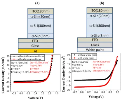
In Fig. 11, the J-V curve is measured for devices with aluminum or white paint back reflectors applied to the backside of the FTO-coated glass substrate for the same sample. The measurement is carried out using a Keithley 2440 5A source meter, Oriel sol3A class AAA solar simulator, and a Forter I-V measurement and analysis system. The sample is diced so that half of it is white paint coated, and the other half is evaporated aluminum. After applying the white paint reflector to the amorphous silicon solar cell, the solar cell efficiency is increased from 5.03% to 9.43%. If an aluminum reflector is used instead, the efficiency is increased from 4.66% to 5.41%. In this experimental setup, an aluminum reflector is used due
to its lower cost and the compatibility with silicon IC processing technology. If a silver reflector is used instead, the efficiency for metal back devices can be slightly higher due to the higher reflectance of silver. Nonetheless, the cost of a silver reflector will be significantly higher, and the efficiency of silver-backed solar cells is not expected to exceed the white paint device, evident from the fact that the white paint device is far more efficient than the aluminum one. Based on our preliminary experimental study, it is suggested that diffuse medium reflectors are, in fact, very promising, due to zero plasmonic loss, low cost, low temperature processing, and high throughput. From this initial experimental verification, it is demonstrated that the concept of diffuse medium reflectors can indeed be applied to future photovoltaics, and by wave optics design and optimization it is believed that reflectance and haze parameters will be continuously improved in the future.
α-Si p(8nm) α-Si i(300nm) α-Si n(20nm) FTO Glass ITO(180nm) Al -0.2 0.0 0.2 0.4 0.6 0.8 1.0 -20 -15 -10 -5 0 5 10 15 20 Jsc=16.62mA/cm2 Voc=0.86V FF=0.66 Efficiency=9.43% C u rre nt De nsi ty (mA /cm 2 ) Voltage(V)
without white paint with white paint Jsc=8.74mA/cm2 Voc=0.84V FF=0.69 Efficiency=5.033% α-Si p(8nm) α-Si i(300nm) α-Si n(20nm) FTO Glass ITO(180nm) White paint (a) (b) -0.2 0.0 0.2 0.4 0.6 0.8 1.0 -20 -15 -10 -5 0 5 10 15 20 Jsc=10.03mA/cm2 Voc=0.78V FF=0.69 Efficiency=5.41% Jsc=8.72mA/cm2 Voc=0.80V FF=0.67 Efficiency=4.66% C urr ent D ens it y( m A /c m 2 ) Voltage(V)
without Aluminum reflector with Aluminum reflector
Fig. 11. (a) J-V with and without an aluminum back reflector. (b) J-V with and without a white paint back reflector. In these measurements, the light comes from the indium tin oxide (ITO) side.
8. Conclusion
In this work, it is shown that dielectric mirrors can provide ultra-broadband high reflectance and light trapping necessary for solar cell application. This can be achieved by properly tailoring aperiodic or randomized designs. The bandwidth provided by such aperiodic or random dielectric mirror designs is significantly larger than the conventional dielectric mirrors such as periodic DBRs or leaky-mode-based broadband high-index-contrast grating (HCG). The side-by-side comparison for various solar cell structures with dielectric or metallic mirrors, at their respective optimized geometry, reveals that the dielectric mirrors are widely applicable to either thin-film or thick wafer-based solar cells. The angular emission plots of time-averaged Poynting vectors further demonstrate that purely dielectric mirrors can still provide efficient light scattering, despite the absence of surface plasmon emission. The observation of the same light-trapping capability for metallic and dielectric mirrors suggests that dielectric mirrors should be employed for future photovoltaics. This is especially true for diffuse medium reflectors, since it possesses the advantage of lower cost, lower temperature processing, higher throughput, and zero plasmonic absorption, with which metallic reflectors can never compete. The preliminary experimental effort also confirms the decent feasibility of
