___________________________________________ 0-7803-8560-8/04/$20.00©2004IEEE
A CMOS Low Dropout Regulator Stable With Any Load Capacitor
Hsuan-I Pan, Chin-Hung Cheng, Chern-Lin Chen, Senior Member IEEE
Department of Electrical Engineering &
Graduate Institute of Electronics Engineering
National Taiwan University
Ta-yung Yang
System General Corp.
Taiwan
ABSTRACT
A CMOS low dropout regulator (LDO) with a new pole-zero pairs cancellation compensation scheme is presented. LDO using this proposed compensation technique provides stable output voltage with any load capacitor. The only constraint on the equivalent series resistance (ESR) of the load capacitor is that it should be less than the load resistance. It is especially suitable for system-on-chip integration applications and board size reduction.
1. INTRODUCTION
Low dropout regulators (LDOs) are widely used for power management applications. Compared with switching regulators, LDOs are less expensive, smaller in size and easier to be used. Moreover, the noise of output voltage is lower and the response to input voltage transient and output load transient is faster. These advantages make LDOs suitable for battery-powered equipments, communication systems, portable systems, and post regulators of switching regulators. Among possible process technologies, CMOS technology is very attractive for LDO circuit implementation because of its low cost, low power consumption and potential for future system-on-chip integration.
One of the most important issues in LDO design is to maintain the system stability. Conventionally, all LDO systems require off-chip load capacitors for stability. In addition to the value of the load capacitor, the capacitor’s parasitic equivalent series resistance (ESR) plays an important role [1]. Most LDOs rely heavily on the ESR value for stability. The basic problem with such LDOs is that the ESR, being parasitic, is not well controlled and not guaranteed by capacitor manufacturers, specifically at low temperatures.
In the literatures, there have been several LDO compensation methods [2~6] presented. These methods mostly focus on improving the performance
of LDO. The ESR and the value of the load capacitor are still limited. A damping-factor-control frequency compensation approach [7] is presented to allow a capacitor-free CMOS LDO.
In this paper, a CMOS LDO using new compensation scheme that can maintain system stability without a load capacitor is proposed. Moreover, it can provide stable output under all load conditions with any value of load capacitor. The ESR of the load capacitor can range from zero to some finite value.
2. REVIEW OF CONVENTIONAL LDO COMPENSATION SCHEME
Fig. 1 shows a conventional LDO system. PMOS is used as the pass element to improve dropout voltage performance without increasing complexity of the circuit [8]. A conventional LDO can be considered a two-stage amplifier connected as a unity gain buffer. The first stage is the error amplifier, and the second stage consists of the pass element with R1, R2, RL,
RESR and CL. Due to high output resistance of the
error amplifier and large CL, there is one low
frequency pole at the output of each stage, respectively. Conventionally, the RESR is utilized to
insert a zero between two low frequency poles and unity gain frequency, as shown in Fig. 2. Normally, R1, R2 are much larger than RL.
Fig. 1 System block of a conventional LDO
266
Fig. 2 Frequency response of the LDO open loop gain with conventional compensation scheme The low frequency poles and ESR zero in open loop transfer function can be estimated as
P1=(2ʌCPARROA) -1
(1) PL=(2ʌCLRL)-1 (2)
ZESR=(2ʌCLRESR)-1 (3)
P1 is the pole at output of the error amplifier stage and
PL is the pole at output of the second stage, CPAR and
ROA are the parasitic capacitance seen at the gate of
the pass element and the output resistance of the error amplifier, respectively. With carefully selected CL
and RESR, ZESR can locate between the unity gain
frequency and two low frequency poles. As ZESR
contributes +90 degrees phase shift, this two-pole one-zero system can provide sufficient phase margin. In this way, the system can be guaranteed stable.
However, there are two major problems in the conventional compensation scheme. First, RESR must
be some finite value therefore the load transient performance cannot be optimized. Second, the value of RESR and CL are strictly limited because DC gain
and frequency of PL of the open loop transfer function
will vary with loading conditions. For example, as load current changes from 1mA to 100mA, transconductance of the pass element may be ten times larger, and RL becomes one hundred times
smaller. As a result, frequency of PL becomes one
hundred times larger and the DC value of the loop gain becomes ten times smaller. In other words, frequency response of the open loop transfer function is different under different loading conditions. So the position of ESR zero is strictly confined in a limited range. That is, RESR and CL must be designed very
carefully.
3. PROPOSED POLE-ZERO PAIRS CANCELLATION COMPENSATION
3.1. Stability of the LDO with Pole-Zero Pairs Cancellation Compensation
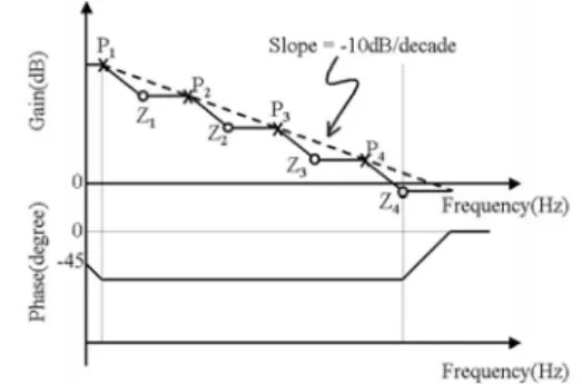
A pole-zero pairs cancellation compensation scheme is proposed to alleviate those conventional design constraints. Fig. 3 illustrates the basic concept of pole-zero pairs cancellation compensation scheme. As a series of pole-zero pairs are generated and arranged appropriately in the open loop transfer
function, a sufficient phase margin can be achieved. The frequency of Zi (i=1 to 4) is designed to be ten
times of Pi. As a result, the phase shift is about 45
degrees over P1 to Z4 because the phase shift of each
pole-zero pair will cancel with each other, and the average slope of loop gain turns out to be –10dB/decade, so a straight line of –10 dB/decade can be used to approximate the curve of gain between P1 and Z4. An LDO using this compensation method
is stable with different CL and RESR conditions. The
detailed discussions of phase margin and stability can be divided into three cases as below.
Fig. 3 Frequency response of the pole-zero pairs cancellation compensation
1) Without an off-chip CL: Without an off-chip CL,
PL moves to higher frequency than unity gain
frequency. As Fig. 4 shows, there are several pole-zero pairs before unity gain frequency, the equivalent slope of gain is –10dB/decade, and PL
does not affect the phase margin due to its high frequency location. The phase margin is about 135 degrees in this case because pole-zero pairs only provide –45 degrees phase shift.
2) With an off-chip CL, without RESR: Off-chip CL
and RL will generate a low frequency pole PL. So
besides –45 degrees phase shift provided by pole-zero pairs, PL contributes at most –90 degrees phase shift.
It results at least 45 degrees phase margin and the LDO remains stable.
3) With an off-chip CL, with RESR: When RESR is
large enough and that cannot be neglected, it will generate a zero ZESR with CL lower than the unity
gain frequency. As Figure 4 shows, ZESR will reduce
the slope of gain and increase the phase shift. If ZESR
is larger than PL, that is, RESR is smaller than RL,
phase margin of LDO will become larger compared to case 2, so LDO is also stable in this case.
In summary, an LDO with this compensation scheme is stable as long as RESR is smaller than RL,
which can be achieved easily. In other words, wherever the position of PL is, phase margin of the
LDO is at least 45 degrees.
267
Fig. 4 Frequency response of the loop gain with different load capacitors
3.2. Pole-Zero Pairs Generation
The pole-zero pair at the lowest frequency can be generated through a parallel amplifier structure or the amplifier with a feed-forward capacitor [8]. However, several pole-zero pairs are needed for pole-zero pairs compensation. A new pass element structure is used to generate pole-zero pairs with designed positions. Fig. 5 shows the proposed pass element structure, where C1~C4 can be parasitic capacitors of M1~M4 or
additional on-chip capacitors. If R(i+1) >> Ri (i=1~3),
the transfer function of VO(s)/VI(s) can be written as
A1/(1+P1)+A2/(1+P2)+A3/(1+P3)+A4/(1+P4) (4)
Ai=gmiRL (i=1~4), Pi=ȈRiCi (i= 1~4)
where gmi is the transconductance of Mi (i=1~4).
If gmi < gm(i+1) (i= 1~3), the frequency response of
|VO(s)/VI(s)| can be approximated by the envelop of
the frequency response of the four terms in equation (4), as the solid line in Fig. 6. So this structure generates three pole-zero pairs in the transfer function of loop gain.
Fig. 5 Proposed pass element structure
Fig. 6 Frequency response of four terms and asymptote of |VO(s)/VI(s)|
3.3. Circuit Implementation
The simplified overall schematic of proposed LDO is shown in Fig. 7. It is composed of a differential amplifier with a feed-forward capacitor and a pass element using proposed structure, where M7 and M8
are biased in triode region to behave as resistors. The VREF is generated by a bandgap voltage reference.
The first amplifier with feed-forward capacitor CC
generates the lowest frequency pole-zero pair. Other pole-zero pairs are generated through the pass element. Due to the average slope of gain without CL
is only –10dB/decade, the DC loop gain cannot be very high because of high frequency parasitic poles. To achieve about 40 dB DC loop gain for acceptable regulation performance, phase margin for worst case is designed to be a smaller value. The simulated phase margin under different load conditions with different CL is shown in Fig. 8 and the phase margin
is designed at least 42 degrees.
Fig. 7 Simplified overall schematic of the LDO
Fig. 8 Simulated phase margin versus CL under
different load conditions
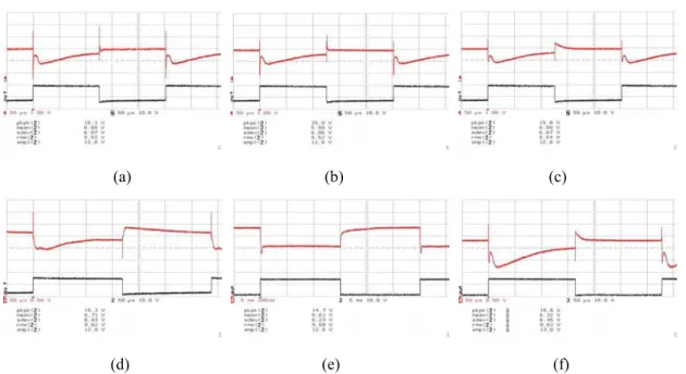
4. EXPERIMENTAL RESULTS
The proposed LDO has been implemented in 0.5-μm 1P2M CMOS technology. It is designed to deliver a maximum load current of 150mA. The preset output voltage is 2.5V. Fig. 9 shows the waveforms of output voltage under load current transients using different load capacitors. The load current changes from zero to 150mA and back to zero with rise and fall times of 2us. As Fig. 9 shows, the output voltage is stable with different load capacitors and ESRs. Listed in Table I are the key performance parameters of the LDO. It is noted that CL value is not
necessarily specified and the ESR stability region
268
(a) (b) (c)
(d) (e) (f) Fig. 9 Experimental transient response with different load capacitor and ESR:
(a) CL=0, ESR=0. (b) CL=10nF, ESR=0. (c) CL=0.1uF, ESR=0.
(d) CL=1uF, ESR=0. (e) CL=47uF, ESR=0.5ȍ. (f) CL=0.1uF, ESR=1ȍ.
ranges from 0 to RL,min. The line and load regulation
performance is not so brilliant due to the relatively low DC loop gain (about 40dB in this work).
5. CONCLUSION
In this paper, the conventional compensation scheme for LDO and its limitation are analyzed. A new compensation technique using pole-zero pairs cancellation is proposed to improve the sable range for the load capacitor and its ESR value. An LDO with new compensation scheme is fabricated and the load capacitor can range from 0 to any value to provide a stable output voltage. The ESR of load capacitor only needs to be less than the load resistance to ensure stability. The measured transient response is quite consistent with the analysis.
Table 1 Performance parameters
Measured Result
VIN 3V~7V
VOUT 2.3~2.5V
Quiescent current 90uA
Dropout voltage 446mV (ILOAD=150mA)
Load regulation 1.47mV/mA
Line regulation 30mV/V
CL stable range Not limited
ESR stable range Smaller than RL,min (16.67ȍ)
6. REFERENCES
[1] C. Simpson, “Linear Regulators: Theory of Operation and Compensation,” Application Note 1148, National
Semiconductor, May 2000.
[2] G. A. Rincon-Mora and P. E. Allen, “Optimized Frequency-Shaping Circuit Topologies for LDO’s,”
IEEE Transactions on Circuits and Systems II, vol. 45,
no. 6, pp. 703-708, Jun. 1998.
[3] K. N. Leung, P. K. T. Mok, and W. H. Ki, “A Novel Frequency Compensation Technique for Low-Voltage
Low-Dropout Regulator,” IEEE International
Symposium on Circuits and Systems, vol. 5, pp.
102-105, May 1999.
[4] W. Chen, W. Ki and P. K. T. Mok, “Dual-Loop Feedback for Fast Low Dropout Regulators,” IEEE
Power Electronics Specialists Conference, vol. 3, pp.
1265-1269, Jun. 2001.
[5] C. K. Chava and J. Silva-Martinez, “A Robust Frequency Compensation Scheme for LDO Regulators,” IEEE International Symposium on
Circuits and Systems, vol. 5, pp. 825-828, May 2002.
[6] K. C. Kwok and P. K. T. Mok, “Pole-Zero Tracking Frequency Compensation for Low Dropout Regulator,” IEEE International Symposium on Circuits
and Systems, vol. 4, pp. 735-738, May 2002.
[7] K. N. Leung and P. K. T. Mok, “A Capacitor-Free CMOS Low-Dropout Regulator With Damping-Factor-Control Frequency Compensation,”
IEEE Journal of Solid-State Circuits, vol. 38, no. 10,
pp. 1691-1702, Oct. 2003.
[8] G. A. Rincon-Mora, “Current Efficient, Low Voltage, Low Drop-Out Regulators”, Ph.D. Thesis, Georgia
Institute of Technology, Nov. 1996.
![Fig. 1 shows a conventional LDO system. PMOS is used as the pass element to improve dropout voltage performance without increasing complexity of the circuit [8]](https://thumb-ap.123doks.com/thumbv2/9libinfo/8862405.245448/1.892.496.748.925.1084/conventional-element-improve-dropout-voltage-performance-increasing-complexity.webp)