Relationships
between
the
crystalline
phase
of
an
IGZO
target
and
electrical
properties
of
a-IGZO
channel
film
Yih-Shing
Lee
a,*
,
Zuo-Ming
Dai
b,
Cheng-I
Lin
c,
Horng-Chih
Lin
caDepartmentofOptoelectronicSystemEngineering,MinghsinUniversityofScienceandTechnology,Hsin-Fong,Hsin-Chu30401,Taiwan,ROC bInstituteofElectronics,MinghsinUniversityofScienceandTechnology,Hsin-Chu30401,Taiwan,ROC
c
InstituteofElectronicsandDepartmentofElectronicEngineering,NationalChiaoTungUniversity,Hsin-Chu300,Taiwan,ROC Availableonline27May2011
Abstract
ThisstudyusedpowderscontainingdifferentIn2O3–Ga2O3–ZnO(IGZO)chemicalcompositionstomanufacturetargetsusingametallurgical process.TheresultingtargetswereusedtodepositamorphousIn–Ga–Zn–O(a-IGZO)channelfilmsbyaradiofrequencymagnetronsputtering process.Thisstudyexaminedtherelationshipsbetweenthesetargetcompositionsandcrystallinephasesofthepowdersandtheresultingmaterial characterization,examiningtheimpactsonelectricalcharacteristicsofa-IGZOfilmswithvariedO2flowrates.Theternarycompoundphaseof ZnGa2O4becamestableat10008CaccordingtoXRDdiagramsatdifferentcalciningtemperatures.AnanalysisoftheXRDdiagramsofdifferent compositionsofIGZOpowdersshowedthattheatomicratioofZnOislargerthanthatofIn2O3andGa2O3,andthatthemainpeaks(101)and (0015)intensityoftherespectiveInGaZnO4andInGaZnO6phasesintensitywouldincrease.Ceramictargetswithdifferentcompositionswere usedtodepositthea-IGZOfilmswithvariedO2flowrates.WhentheO2flowratewaszero,theresultsofaHallmeasurementofa-IGZOfilms depositedfromtargetswithhigherZnatomicratioshowedlowerresistivity,highercarrierconcentration,andlowermobility.Nevertheless,asthe O2flowratewasmorethan5sccm,increasingtheatomratioofZnintheIGZOceramictargetobviouslyincreasedthecapabilityofcapturingO2in thea-IGZOfilms,leadingtohigherresistivity,lowercarrierconcentration(<1018cm 3),andhighermobility.
#2011ElsevierLtdandTechnaGroupS.r.l.Allrightsreserved.
Keywords:A.Films;B.X-raymethods;C.Electricalproperties;IGZO
1. Introduction
Transparent amorphous oxide semiconductors (TAOSs)are promisingforchannelmaterialsofthin-filmtransistors[1](TFTs) andareusedprimarilyfordrivingTFTsinorganiclight-emitting diodedisplaysduetolargemobilities(>10cm2V 1s 1)andlow processtemperatures.SeveralTAOSs,suchasamorphousIn–Ga– Zn–O(a-IGZO)[1–3],In–Zn–O[4,5],Zn–Sn–O[6],andIn–Sn– O[7],havebeenreportedaschannelmaterialsofTFTstodate.As such, an essential feature of TAOSs is that they are multi-componentmaterials,and,thereforehavealargeflexibilitytotune propertiesfor TFTs.However, thisfeatureraises aproblemin determiningthe optimalchemicalcompositionand fabrication conditioninsuchalargeparameterspace.Therefore,werequire anefficienttechniquetosurveysystematicallyamaterialovera
widechemicalcompositionandunderdepositionconditionsfor theactivelayersoftheTFTs.
Moreover, themost vitalcharacteristicfor device applica-tionsisthatthecarrierconcentrationmustbecontrolledatlow levels, forexample,<1015cm 3,withfavorable stabilityand reproducibility to control device characteristics, such as thresholdvoltage,andtosuppresstheoff-current[3].Powder targetsdegradecrystalgrowthqualityofZnOfilms;therefore, ceramic targets were prepared for a-IGZO film by an RF sputtering system [8]. This paper reports the relationships between the crystalline phases of different compositions of In2O3–Ga2O3–ZnO (IGZO) targets and the Hall electrical propertiesofa-IGZOchannelfilmpreparedbyRFmagnetron sputteringwithvariedO2flowrates.
2. Experimentalprocedure
The different composition of IGZO powder used in the experimentwasmixedbytheatomicratiosofIn:Ga:Zn=2:2:1,
www.elsevier.com/locate/ceramint
Available online at www.sciencedirect.com
CeramicsInternational38S(2012)S595–S599
*Correspondingauthor.Tel.:+886355931423383;fax:+88655931423388. E-mailaddress:yslee@must.edu.tw(Y.-S.Lee).
0272-8842/$36.00#2011ElsevierLtdandTechnaGroupS.r.l.Allrightsreserved. doi:10.1016/j.ceramint.2011.05.105
1:1:1,and1:1:2.The powderswerethenmilled, followedby calciningatvarioustemperaturesof730,930,and10308Cfor 1h, respectively. Next, the powders were ground, sieved througha250-meshscreen,andwereformedinto thesputter targetwiththe pressureof 60,000–70,000kg/cm2at 12508C for1hinanArambient.Thea-IGZOfilmsweredepositedat roomtemperature using an RF magnetron sputtering system (LJUHVLJ-303CL)ontheglasssubstratesofSCHOTTB270. Inthedepositionprocess,thesputteringpowerwassetat250W and the working pressure was controlled at 5E 3Torr. Additionally,thesputteringconditionsofa-IGZOfilmwereset atthefixedArflow(50sccm)withvariedO2flowrates(0sccm, 2sccm,5sccm,7sccm,and 10sccm). Afterdeposition, the samples were annealed at 4008C with5E 3Torr working pressurefor 1h inN2ambientof 40sccm.
The crystallinities of different IGZO powders were also analyzedbyXRD(X-Raydiffraction)(PANalyticalX’PertPro) with a Ni-filtered Cu Ka (l=1.5418A˚ ) source in u–2u scanningmode.Thescanninganglewasbetween208and808. HallmeasurementwasutilizedwiththevanderPauwmethod byusingtheHL5500PC(Bio-Rad).Themagneticfieldapplied inthemeasurementwasat0.323T.Thetestsampleswerecut intosquares1cm2.Thefilmsheetresistanceandthicknesswere measured by a 4-point probe (Napson RT-80) and an N&K1500,respectively.
3. Results anddiscussion
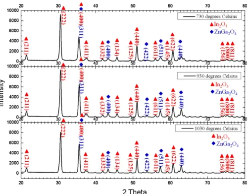
Fig. 1 shows XRD diagrams of IGZO1 (In2O3 :-Ga2O3:ZnO=2:2:1) powders that were calcined at different temperaturesof 730, 930, and 10308C for 1h, respectively.
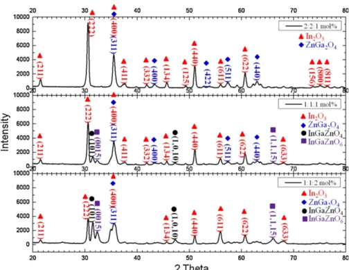
DifferentphaseorientationsofIn2O3andZnGaO4areindicated inFig.1.Beyondthecalcinationstemperatureof10008C,the main phase orientation (222) peak of In2O3decreased, and thosepeaks(400),(511),and(440) intensityofZnGa2O4 increased and saturated. This implied that the ternary compounds ofZnGa2O4reacted completelyand thosepeaks were similar with the XRD results of ZnGa2O4 targets, as measuredaccording toKrishna etal.[9].Fig.2 showsXRD diagrams of IGZO powders with different atomic ratios of In:Ga:Zncalcined at7308C for1h.Differentphase orienta-tions of In2O3, ZnGa2O4, InGaZnO4, and InGaZnO6 are indicatedinFig.2.WhentheatomicratioofZnO waslarger than that of In2O3 and Ga2O3, the main peaks (101) and (0015) intensityof the respectiveInGaZnO4and InGaZnO6 phasesintensityincreased.Thosepeakswerealsoshowninthe XRD patternsof the InGaZnO4target[10].Nevertheless,the mainpeaks(222)and(311)intensityoftherespectiveIn2O3 andZnGa2O4phasesdecreased graduallyas the ZnO atomic ratioincreased.
Fig.3 shows the Hall measurement plot of a-IGZO1film (In:Ga:Zn=2:2:1)asafunctionofO2flowrateswithafixedAr flow, 50sccm.The resistivity increasedlinearly with the O2 flowratefirst,andthenreachedsaturationatthehighO2flow rate [2,11]. By increasing the O2 flow rate, the carrier concentrationdecreasedatthelowerO2flowrate(<5sccm), sccm), but thecarrier concentration increasedatthe highO2 flow rate condition (>5sccm). At the high O2 flow rate condition (>5sccm), the concentration and the mobility becameatrade-offduetothescatteringoftheoxygenvacancy andwhetherthegraindensitywastightornot.Fig.4showsthe SEMgraphsfora-IGZO1filmwiththedepositionconditionat
Fig.1. XRDdiagramsofIGZO1(In2O3:Ga2O3:ZnO=2:2:1)powderswerecalcinedatdifferenttemperaturesfor1h,differentphaseorientationsofIn2O3and
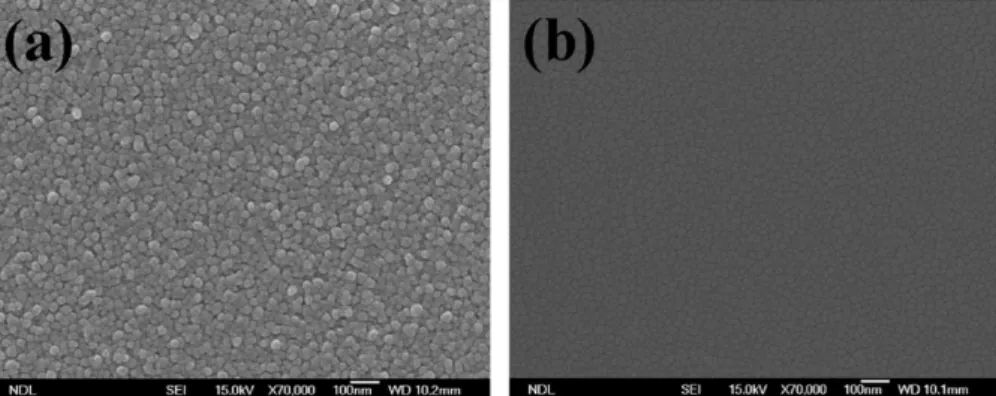
O2flowat0 and2sccm,respectively.It canbeseenthatthe sampleaddedelementofO2appearslooserinthefilm,ascribed toincompletesurfacereactioninthefilmduetolesscontentof Zn in the a-IGZO1 target. Less content of Zn decreases the capability of O2 capture. Therefore,loose appearance inthe surfaceindicateslowermobility.Fig.5showstheSEMgraphs for a-IGZO2 film (In:Ga:Zn=1:1:1) with the deposition conditionatO2flowat0and2sccm,respectively.The result ofa-IGZO3(In:Ga:Zn=1:1:2)isthesameasthatofa-IGZO2. Adequate content of Zn existed in the film; therefore, the capability of O2capturewas promotedandthe surface could reactcompletelyanddisplaydenselywhentheO2wasadded. Afterward, the mobility rose withthe addedO2 flow. Fig.6 shows the Hall measurement plot of a-IGZO2 film (In:Ga:Zn=1:1:1)asafunctionofO2flowrateswithafixed Arflowequalto50sccm.By increasingtheO2flowrate,the carrier concentrationfirst decreasedatthelowerO2flowrate (<5sccm), thenslightly increasedatthe higher O2flowrate
Fig.2. XRDdiagramsofIGZOpowderswiththedifferentatomicratiosofIn:Ga:Zncalcinedat7308Cfor1h,differentphaseorientationsofIn2O3,ZnGa2O4,
InGaZnO4,andInGaZnO6wereindicatedinthediagram.
O2 flow(sccm) 12 10 8 6 4 2 0 Resistivity(ohm-cm) 10-3 10-2 10-1 100 101 Concentration(1/cm 3) 1017 1018 1019 1020 Mobility(cm 2/v-s) 10-1 100 101 102 Resistivity Concentration Mobility IGZO1
Fig.3. Hallmeasurementplotofa-IGZO1film(In:Ga:Zn=2:2:1)asafunction ofO2flowrateswithfixedArflow,50sccm.
condition (>5sccm); finally, the carrier concentration decreased at the highest O2 flow rate (>7sccm). Increasing theatomicratioofZnintheIGZOceramictargetincreasedthe capabilityofcapturingO2,leadingtolowercarrier concentra-tion.Fig.7showstheHallmeasurementplotofa-IGZO3film (In:Ga:Zn=1:1:2)asafunctionofO2flowrateswithafixedAr flowequalto50sccm.Theresistivityrosewiththeincreasing O2flowanddidnotsaturatewhentheO2flowratewasmore than 5sccm. Increasing the atom ratio of Zn in the IGZO
ceramictargetobviouslyincreasedthecapabilityofcapturing O2,leadingtolowercarrierconcentration(<1018cm 3)atthe O2flowrateequalto5sccm.Lowercarrierconcentrationmust be controlled at low levels to control TAOSs–TFT device characteristicswithfavorablestabilityandreproducibility.The resistivity of a-IGZO3 film at the highest O2 flow rate (>7sccm)wasrevealedtobemorethan38.4Vcm,ascribedto thelargestcapability ofcapturingO2.WhentheO2flowrate waszero,the resultsof aHallmeasurement ofa-IGZO films depositedfromtargets withahigher Znatomicratioshowed lower resistivity, higher carrier concentration, and lower mobility.
4. Conclusions
TosummarizeacomparisonoftheXRDanalysesofpowder and Hall measurements of a-IGZO films suggests that increasing the zinc ion content, causes the main peaks (101) and (0015) intensity of the respective InGaZnO4 andInGaZnO6phasesintensity,toincreaseinproportiontothe conductivityandcarrier concentrationina-IGZO filmsatO2 flowrateequaltozero.The resistivityof a-IGZOfilmwitha smallerZnOatomicratiosaturatedwhentheO2flowincreases. LesscontentofZndecreasesthecapabilityof O2capture.By increasingtheO2flowrate,thecarrierconcentrationdecreases on the lower O2 flow rate (<5sccm), but the carrier concentration increases at the high O2 flow rate condition (>5sccm).Nevertheless,theresistivityofa-IGZOfilmwitha higher Znatomicratiorises withthe increasingO2flow and does notsaturatewhen theO2flowrateismorethan5sccm. IncreasingtheatomicratioofZnOinIGZOpowderobviously increases the capability of capturing O2, leading to higher resistivityandlowercarrier concentration.
Acknowledgements
This work was supported by National Science Council Research Project (NSC 98-2218-E-159-002). Hall measure-mentandallothersmeasurementwereimplementedinNCTU and National Nano Device Laboratory, Hsin-Chu, Taiwan, respectively. Authors also thanks for the proof reading this articlefromWallaceAcademicEditing.
Fig.5. SEMgraphsofa-IGZO2film(In:Ga:Zn=1:1:1)withO2flowratesat(a)0and(b)2sccm,respectively.
O2 flow(sccm) 12 10 8 6 4 2 0 Resistivity(ohm-cm) 10-3 10-2 10-1 100 101 Concentration(1/cm 3) 1017 1018 1019 1020 1021 Mobility(cm 2/v-s) 100 101 102 Resistivity Concentration Mobility IGZO2
Fig.6. Hallmeasurementplotofa-IGZO2film(In:Ga:Zn=1:1:1)asafunction ofO2flowrateswithfixedArflow,50sccm.
O2 flow(sccm) 12 10 8 6 4 2 0 Resistivity(ohm-cm) 10-3 10-2 10-1 100 101 102 103 104 Concentration(1/cm 3) 1017 1018 1019 1020 1021 Mobility(cm 2/v-s) 100 101 Resistivity Concentration Mobility IGZO3
Fig.7. Hallmeasurementplotofa-IGZO3film(In:Ga:Zn=1:1:2)asafunction ofO2flowrateswithfixedArflow,50sccm.
References
[1] K.Nomura,H.Ohta,A.Takagi,T.Kamiya,M.Hirano,H.Hosono, Room-temperaturefabricationoftransparentflexiblethin-filmtransistorsusing amorphousoxidesemiconductors,Nature432(2004)488–492. [2] H.Yabuta,M.Sano,K.Abe,T.Aiba,T.Den,H.Kumomi,K.Nomura,T.
Kamiya,H.Hosono,High-mobilitythin-filmtransistorwithamorphous InGaZnO4channelfabricatedbyroomtemperaturerf-magnetron
sputter-ing,AppliedPhysicsLetters89(2006), 112123-1-112123-3. [3] K.Nomura,A.Takagi, T.Kamiya,H.Ohta,M.Hirano,H.Hosono,
Amorphousoxidesemiconductorsforhigh-performanceflexible thin-filmtransistors,JapaneseJournalofAppliedPhysics45(2006)4303– 4308.
[4] N.L.Dehuff,E.S.Kettenring,D.Hong,H.Q.Chiang,J.F.Wager,R.L. Hoffman,C.H.Park,D.A.Keszler,Transparentthin-filmtransistorswith zincindiumoxidechannellayer,JournalofAppliedPhysics97(2005), 064505-1-064505-5.
[5] B. Yaglioglu, H.Y. Yeom, R. Beresford, D.C. Paine, High-mobility amorphousIn2O3–10wt% ZnOthin film transistors, AppliedPhysics
Letters89(2006), 062103-1-062103-3.
[6] R.L.Hoffman,Effectsofchannelstoichiometryandprocessing tempera-tureontheelectricalcharacteristicsofzinctinoxidethin-filmtransistors, Solid-StateElectronics50(2006)784–787.
[7] T.Miyasako,M.Senoo,E.Tokumitsu,Ferroelectric-gatethin-film tran-sistorsusingindium-tin-oxidechannelwithlargechargecontrollability, AppliedPhysicsLetters86(2005), 162902-1-162902-3.
[8] X.Q. Weia, Z. Zhanga, Y.X.Yub, B.Y.Manc, Comparativestudy on structuralandopticalpropertiesofZnOthinfilmspreparedbyPLDusing ZnOpowdertargetandceramictarge,Optics&LaserTechnology41 (2009)530–534.
[9] K.M.Krishna,M.Nisha,R.Reshmi,R.Manoj,A.S.Asha,M.K.Jayaraj, ElectricalandopticalpropertiesofZnGa2O4thinfilmdepositedbypulse
laserdeposition,MaterialsForum29(2005)243–247.
[10] M.Orita,M.Takeuchi,H.Sakai,H.Tanji,Newtransparentconductive oxideswithYbFe2O4structure,JapaneseJournalofAppliedPhysics34
(1995)L1550–L1552.
[11] Y.K. Moon, S. Lee, D.H. Kim, D.H. Lee, C.O. Jeong, J.W. Park, ApplicationofDCmagnetronsputteringtodepositionofInGaZnOfilms forthinfilmtransistordevices,JapaneseJournalofAppliedPhysics48 (2009)031301–031304.