An optimal silicidation technique for electrostatic discharge
protection sub-100 nm CMOS devices in VLSI circuit
Shao-Ming Yu
a, Jam-Wen Lee
b, Yiming Li
c,*aDepartment of Computer and Information Science, National Chiao Tung University, Hsinchu 300, Taiwan bMicroelectronics and Information Systems Research Center, National Chiao Tung University, Hsinchu 300, Taiwan
c
Department of Communication Engineering, National Chiao Tung University, Hsinchu 300, Taiwan Available online 20 March 2006
Abstract
In this paper we propose a silicide design consideration for electrostatic discharge (ESD) protection in nanoscale CMOS devices. According to our practical implementation, it is found that a comprehensive silicide optimization can be achieved on the gate, drain, and source sides with very few testkey designs. Our study shows that there is a high characteristic efficiency for various conditions; in particular, for optimizing the performance of sub-100 nm complementary metal-oxide-semiconductor devices in system-on-a-chip era. Ó 2006 Elsevier B.V. All rights reserved.
Keywords: Electrostatic discharge; Silicide; Nanoscale device; VLSI circuit; System-on-a-chip; Modeling; Simulation; Optimization
1. Introduction
Electrostatic discharge (ESD) is an important issue in complementary metal-oxide-semiconductor (CMOS) cir-cuit design and manufacture; in particular, for the sub-100 nm technology era[1–6]. Simultaneously scaling down of the gate oxide, source-drain and silicide suffer ESD robustness[2]. An optimization of ESD protection devices will obtain a good ESD robustness. Among these device parameters, silicide is the most important factor for its ESD robustness. Change of silicidation can be achieved by directly adding a low cost photo-mask [3]. To reduce the cost and complexity of testkey design, most of the opti-mizations have been done on drain side by designing a ser-ies of testkeys possessing a non-silicide region with various widths and locations. However, it is known that an optimi-zation of drain side is not enough[5]. Performing optimiza-tion on drain, source, and gate sides are necessary. Contrary to conventional ways, to optimize silicides on electrodes aforementioned, we study here a different
opti-mization methodology. To investigate the device internal electric field distribution and carrier temperature for advanced ESD design, we simulate the device transport properties with a set of semiconductor device equations that include Poisson equation, electron-hole current conti-nuity equation, and electron-hole energy conservation equation [4,7]. Based on our experiment and simulation study, we conclude that our approach provides an alterna-tive for the optimization of the silicide by exploring the local current density, maximum electric field and tempera-ture gradient. This method accounts for the failure mecha-nism of the devices successfully. Besides the device optimization for ESD robustness, the circuit optimization strategy is also achieved on the ESD strength, standby cur-rent consideration, driving capability, and operation speed. This paper is organized as follows. Section 2 states device structure, measurement, and simulation. Section 3 dis-cusses the results. Finally, we draw conclusions.
2. Device structures and characterization
The explored devices are fabricated using 90 nm CMOS technology, their cross-section views are shown in Fig. 1. The layout parameters are listed in Table 1. Oxide
0167-9317/$ - see front matter Ó 2006 Elsevier B.V. All rights reserved. doi:10.1016/j.mee.2006.02.006
*
Corresponding author. Present address: P.O. Box 25-178, Hsinchu 300, Taiwan. Tel.: +886 930 330 766; fax: + 886 572 6639.
E-mail address:[email protected](Y. Li).
thickness of this technology is 1.6 nm and the source and drain silicides are formed by using cobalt to have a thick-ness about 30 nm. All of our test structures have a gate length of 120 nm. Transmission line pulse generator (TLPG) measurement used to characterize ESD robustness of our test structures is done by using Barth Electronics Model 4002 TLP. In good agreement of the industry stan-dard-Human Body Model (HBM); the pulse for measure-ment is 100 ns, whose raise time and fall time are controlled within 20 ns HP 4156B semiconductor analyzer is used to measure quasi-static current-voltage (IV) proper-ties of the devices. Finally, the HP 4284 capacitance voltage analyzer is used to verify the high frequency capacitance-voltage (CV) characteristics of the silicided and non-sili-cided gate devices.
The designed device structures are simulated with a two-dimensional (2D) hydrodynamic (HD) device simulation prototype[4,7], where the devices’ internal transport phe-nomena and terminal characteristics are investigated and compared. In the simulation, a set of 2D HD device
equa-tions including the Poisson, carrier current continuity, car-rier energy balance, and lattice temperature equations is solved numerically. First of all, the HD equations are decoupled and each decoupled equation is solved sequen-tially to obtain ‘‘self-consistent’’ solution. To solve each decoupled equation efficiently; we apply the adaptive com-putational algorithm for each equation. This simulation technique has been successfully proposed for deep-submi-cron MOSFET and DTMOSFET simulation in our recent works[7]. With the developed device simulation prototype, we simulate the proposed devices to evaluate the character-istics for ESD design, where the calculations of device elec-tric field, internal temperature, and current density are included. Comparison of these physical quantities among these devices is performed; as a result, a suitable device could be characterized and advised.
3. Results and discussion
Fig. 2shows the characteristics of drain current versus gate voltage (Id-Vg) of the three experimental devices; the device B has a relatively lower threshold voltage than the others. The main reason can be explained by high fre-quency CV characteristics, shown in Fig. 3, that the flat band voltage of the non-silicided gate (device B) is higher than the silicided gate (devices A and C). Furthermore, this figure also indicates that the inversion capacitance of the non-silicided one is higher than the silicided one. Results are caused from the poly-depletion effect. This effect is caused from the fact that doping concentration of the non-silicided gate is higher than the silicided gate[4], which lowers the threshold voltage of the device B. However, the threshold voltage lowering effect is a serious problem that enlarges the leakage current of the ESD protection circuits. According to our estimations, the silicidation related threshold lowering effect could be as large as 70 mV and may lead to a leakage current with one order magnitude.
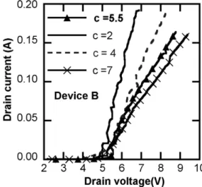
The TLPG curve of the three devices is shown inFig. 4. It is found that the device B has a better ESD robustness among structures. Higher resistance of the non-silicided gate sustains a higher breakdown voltage of gate oxide under TLPG measurement despite a similar breakdown voltage with DC method.Fig. 5indicates that the non-sili-cided width at drain side significantly modulates the turn-on resistance of the protection devices. However, there is only
Fig. 1. Cross-section views for the three tested device structures.
Table 1
A list of layer parameters for the three tested device structures
a (lm) b (lm) c (lm) d (lm)
A 0.26 0.3 5.5 1
B NA 0.3 5.5 1
C 0.26 0.3 5.5 0.11
Parameters:
a: Poly-Si gate to SAB spacing.
b: Contact to silicide blocked layer spacing. c: Contact to Poly-Si gate spacing at drain side.
slight influences on ESD robustness when the width is larger than 1 lm. It is found that the electric field distributions of all devices, shown inFig. 6, are very similar. When varying the value of parameter c,Fig. 6shows the maximum electric field of the device B occurred at the region of anti-punch through implant. Obtained results indicate the importance of optimization of drain side silicide in area consideration and the efficiency of ESD protection. The efficiency of ESD protection circuit dominates the ESD robustness of the non-protection circuits. Poor efficiency of the protection circuit results in charges flowing through the core circuit rather than the protection circuit. High turn-on resistance of protection devices may damage core circuits.
According to our investigation, optimization of ESD protection device will benefit VLSI circuit manufacturing. In order to lower the development cost of the ESD protec-tion devices, an accurate device simulaprotec-tion is applied. It enables us to predict the silicide effects at drain side and
Fig. 2. A plot of quasi-static IV characteristic for the three ESD protection devices.
Fig. 3. High frequency CV characteristic for silicided and non-silicided ESD protection devices.
Fig. 4. A plot of TLPG IV characteristics for the explored three ESD protection devices.
Fig. 5. TLPG IV characteristic for the type B ESD protection device with different parameter c.
provides a simple way in optimizing the silicides. Unlike the non-silicided width at drain, Fig. 7shows the non-sili-cided width at source will degrade the ESD robustness when the width larger than 1 lm. It results from a negative source-substrate bias when devices turned on. Therefore, it reduces the efficiency of parasitic bipolar junction transis-tor that plays a central role in conduction ESD current. Finally, it causes a poor ESD strength. After stressing device into breakdown by TLP, a series of DC measure-ments are performed to verify failure location of those devices. The result demonstrates that device A may have a strong damaged source region. The device C is ruined at drain side. The device B has a slight damage at drain side. While performing the TLP stressing, the channel properties of the three devices are also characterized and are found no degradations before breakdown. Damages are caused from multiplication effects but not accumulation effects.
Devices’ temperature profiles at the source side are also simulated as shown in Fig. 8. It is consistent with the previously result that the device C has a failure point caused from the localized temperature distribution at the source side interface. For the structure of device C with very narrow source region, electrons are crowding at this region. It results in damages at the source side. This result is also indicated that the optimization should be considered at drain and source side. Fig. 9 recommends a whole chip design for the silicide optimization. The device B can be used as the input protection and power clamp circuits for the better ESD robustness. However, to pursue lower standby leakage current, a control circuit is required. For the considerations of speed and driving capability, the devices A and B are not good for the output buffer circuit. Therefore, the device C with a diode pair is more suitable for the output driver network.
4. Conclusions
We have studied a silicide optimization for electrostatic discharge protection devices in nanoscale CMOS circuit design. Device simulation on the structures has shown that a silicide optimization can be achieved on the gate, drain, and source sides with few testkey designs. Fabrication, measurement, and simulation have demonstrated our approach has high characteristic efficiency for various con-ditions. Studies on the devices A–C provide an alternative in sub-100 nm circuit design. A circuit level ESD design has also been discussed for the system performance and speed evaluation.
Acknowledgments
This work was supported in part by the National Sci-ence Council of Taiwan under Contract NSC-94-2215-E-009-084 and Contract NSC-94-2752-E-009-003-PAE, and by the Ministry of Economic Affairs, Taiwan under Con-tract 93-EC-17-A-07-S1-0011. J.-W. Lee thanks United Microelectronic Corp. in Hsinchu, Taiwan for device fabri-cation and measurement.
Fig. 7. TLPG IV characteristic for type B ESD protection device with different parameter d.
Fig. 8. A plot of normalized temperature profile at the source side of device C.
References
[1] A. Salman, R. Gauthier, W. Stadler, K. Esmark, M. Muhammad, C. Putnam, D.E. Ioannou, in: Proceedings of International Reliability Physics Symposium (IRPS), 2001, p. 219.
[2] W. Fichtner, K. Esmark, W. Stadler, in: Technical Digest of International Electron Devices Meeting (IEDM), 2001, p. 311. [3] M.-D. Ker, H.-C. Jiang, in: Proceedings of IEEE Conference on
Nanotechnology, 2001, p. 325.
[4] Y. Li, J.-W. Lee, S.M. Sze, Japanese Journal of Applied Physics 42 (Part 1) (2003) 2152.
[5] A. Salman, R. Gauthier, W. Stadler, K. Esmark, M. Muhammad, C. Putnam, D.E. Ioannou, IEEE Transactions on Device and Materials Reliability 2 (2002) 2.
[6] J.-W. Lee, Y. Li, in: Proceedings of IEEE Conference on Nanotech-nology, 2003, p. 639.
[7] Y. Li, S.M. Sze, T.-S. Chao, Engineering with Computers 18 (2002) 124.