Study of boron effects on the reaction of Co and Si 1x Ge x at various temperatures
H. J. Huang, K. M. Chen, C. Y. Chang, T. Y. Huang, T. C. Chang, L. P. Chen, and G. W. Huang
Citation: Journal of Vacuum Science & Technology A 18, 1448 (2000); doi: 10.1116/1.582368 View online: http://dx.doi.org/10.1116/1.582368
View Table of Contents: http://scitation.aip.org/content/avs/journal/jvsta/18/4?ver=pdfcov
Published by the AVS: Science & Technology of Materials, Interfaces, and Processing
Articles you may be interested in
Thermal reaction of nickel and Si 0.75 Ge 0.25 alloy
J. Vac. Sci. Technol. A 20, 1903 (2002); 10.1116/1.1507339
Study on Ge/Si ratio, silicidation, and strain relaxation of high temperature sputtered Co/Si 1x Ge x structures
J. Appl. Phys. 88, 1831 (2000); 10.1063/1.1305832
Phase formation and strain relaxation during thermal reaction of Zr and Ti with strained Si 1xy Ge x C y epilayers
J. Appl. Phys. 88, 1418 (2000); 10.1063/1.373833
Effects of composition on the formation temperatures and electrical resistivities of C54 titanium germanosilicide in Ti–Si 1x Ge x systems
J. Appl. Phys. 86, 1340 (1999); 10.1063/1.370892
Thermal stability and electrical properties of Zr/Si 1xy Ge x C y contacts after rapid thermal annealing
Àx x
at various temperatures
H. J. Huang, K. M. Chen, C. Y. Chang,a)and T. Y. Huang
Department of Electronic Engineering and Institute of Electronics, National Chiao-Tung University, Hsin-chu 30050, Republic of China
T. C. Chang, L. P. Chen, and G. W. Huang
National Nano Device Laboratory, Hsin-Chu, Republic of China 共Received 16 August 1999; accepted 10 January 2000兲
The effects of boron on Co and Si1⫺xGex interfacial reaction were studied. Undoped and in situ
boron-doped strained Si0.91Ge0.09and Si0.86Ge0.14layers prepared at 550 °C by an ultrahigh vacuum chemical vapor deposition system were subjected to Co silicidation at various rapid thermal annealing共RTA兲 temperatures ranging from 500 to 1000 °C. The resulting films were characterized by a sheet resistance measurement, Auger electron spectroscopy, x-ray diffractometry共XRD兲, high resolution x-ray diffractometry, secondary ion mass spectroscopy, scanning electron microscopy, and transmission electron microscopy. Seen from XRD spectroscopy, a Co(Si1⫺yGey) cubic
structure was formed with RTAs ranging from 500 to 700 °C. For boron-doped samples, the CoGe fraction in Co(Si1⫺yGey) was less than that in undoped samples, indicating that boron atoms
retarded the incorporation of Ge into the Co(Si1⫺yGey) ternary phase. It also led to a large Ge
pileup at the interface between the Co-rich and silicidation regions. On the other hand, from the high resolution x-ray spectra, the presence of boron led to less relaxation of the strained Si1⫺xGexlattice.
It is the first time that small boron atoms inhibiting the relaxation of the Si1⫺xGex layer during
silicidation was observed. Furthermore, from the sheet resistance measurement, the formation of CoSi2was found to be slightly retarded in boron-doped samples, due probably to the decrease of Co or Si diffusivities as a result of boron accumulation at the Co/SiGe reaction interface. At temperatures above 800 °C, CoSi2 formed and Ge segregated to the silicide boundaries and the upper reaction region was discovered. These phenomena caused by B dopants are explained in detail. © 2000 American Vacuum Society. 关S0734-2101共00兲04604-2兴
I. INTRODUCTION
Silicided strained-Si1⫺xGex junctions have attracted lots
of attention because of their potential applications to band-gap engineering by varying the Ge fraction in the Si1⫺xGex
layer. Recently advanced device structures based on the Si1⫺xGex/Si heterojunction have been demonstrated.1–4 In many device applications, it is necessary to make Schottky or ohmic contact with the epitaxial Si1⫺xGex alloys. One example is the use of silicided strained-p-Si1⫺xGexjunctions in infrared detectors. With the addition of Ge in the strained Si1⫺xGex layer, it is feasible to modulate and extend the
cutoff wavelength.5 Significant efforts have thus been made to understand the phase formations and properties of metal/ Si1⫺xGex reactions.6–16
Among the potential metal silicides, CoSi2 is particularly attractive for its low resistivity, cubic crystal structure, rela-tively small lattice mismatch with Si, and its compatibility with the self-aligned silicide共salicide兲 scheme. At room tem-perature, the resistivity of CoSi2and its lattice constant mis-match with Si are 16 ⍀ cm and 1.2%, respectively. Three cobalt silicide phases, i.e., Co2Si, CoSi, and CoSi2, form in sequence when a Co/Si bilayer structure is annealed.17,18The formation temperatures of CoSi and CoSi2 are ⬃400 and 550 °C, respectively. In addition, Co5Ge7and CoGe2 phases
are formed after annealing a Co/Ge bilayer structure at tem-peratures of about 300 and 600 °C, respectively.12,19 In the past few years, the reaction of the Co/strained-Si1⫺xGex/Si
system has been studied extensively.11,12,15,16Compound for-mation after thermal treatment and the stability of the strained Si1⫺xGexlayer during silicide formation were
inves-tigated. For the ternary phase diagram of the Co–Si–Ge sys-tem, a miscible ternary compound, Co(Si1⫺yGey) ( y ⬍0.67), was found after low temperature furnace annealing 共in the range from 400 to 700 °C兲, which is based on the
cubic CoSi structure.20 However, the crystal structures of CoSi2 共i.e., the cubic CaF2 structure兲 and CoGe2 共i.e., the orthorhombic structure兲 are different, and the reaction be-tween Co and Si is favored more than the Co–Ge one. As a result, only the CoSi2 phase is observed at higher tempera-tures共⬃ 700 °C by furnace annealing兲. Concurrently, surface accumulation of Ge in the form of Ge-rich Si1⫺zGez precipi-tates is observed.14,21
The strained SiGe layer is widely used as the base in heterojunction bipolar transistors and as the raised source/ drain in advanced metal–oxide–semiconductor 共MOS兲 tran-sistors. For such applications, the Si1⫺xGex layer is usually
heavily doped. Dopants will redistribute in the reaction re-gion or may even affect the metal/Si1⫺xGexreaction during
thermal processing. The effects of high dopant concentration on the Co silicidation process and the redistribution of dop-a兲Electronic mail: u8511522@cc.nctu.edu.tw
ants during silicidation were studied.22Surface accumulation of boron redistributed from the Si consumption layer was observed. Furthermore, a comparison between B and Sb dop-ants in Co/Si0.8Ge0.2 during silicidation was reported recently.23 While both dopants were found to accumulate at the surface, boron atoms were also found to be trapped at the interface between the Co-rich surface layer and the monosi-licide region. In addition, a significant accumulation of Ge between the unreacted SiGe and the silicided region was ob-served on boron-doped Si0.8Ge0.2samples, suggesting that B and Ge redistributions occur. However, a detailed explana-tion of boron impact on Co/Si1⫺xGex compound formation
and Ge redistribution due to lattice relaxation is, to the best of our knowledge, still has not been given.
In this article, we study the interfacial reaction of Co with the strained Si1⫺xGex layer, especially the effects of boron
dopants on compound formation and lattice relaxation during silicidation. The phase formation at various rapid thermal annealing共RTA兲 temperatures and the structural characteris-tics were also examined. This study will be helpful for future device applications in Si1⫺xGex heterojunction bipolar
tran-sistors and advanced MOS trantran-sistors with a raised silicided Si1⫺xGex source/drain.
II. EXPERIMENTS
Strained single-crystal Si1⫺xGex thin films with x⫽0.14
and 0.09 were grown by an ultrahigh vacuum chemical vapor deposition 共UHVCVD兲 system.24 The UHVCVD system in-cluded a loading chamber, a water-cooled stainless-steel growth chamber, separate nozzles for process gases, and a computer-controlled gas switching box. The growth chamber was pumped with a 1000 l/s turbomolecular pump to a base pressure of 2⫻10⫺10Torr. As the starting substrates 10–15
⍀ cm, n-type 共100兲 silicon wafers were used. The wafers
were first subjected to a pre-clean process using a hydrogen passivation technique. Afterwards, the wafers were loaded into the loading chamber and pumped down to 10⫺6Torr with minimal delay. The wafers were then immediately transferred into the growth chamber for epitaxial growth. During the transfer process, the heater temperature was kept at 200 °C. A base pressure of 10⫺9Torr was routinely ob-tained within 1 min of the wafer transfer process. Then, the wafers were heated to the final deposition temperature of 550 °C at a ramp rate of⬃150 °C/min. For growing undoped Si1⫺xGex, pure Si2H6 and GeH4 were introduced into the growth chamber. For growing in situ boron-doped Si1⫺xGex,
a 1% B2H6gas diluted in H2was added. The resultant boron concentration in the in situ boron-doped SiGe samples was found to be 1⫻1019cm⫺3, while the unintentionally doped
共i.e., undoped兲 samples have a low boron doping level of
about 1⫻1015cm⫺3. The chamber pressure was maintained below 10⫺3Torr during epitaxial growth by the turbomo-lecular pump. The grown Si1⫺xGex epitaxial layer thickness
was 100 nm for all samples used in this study.
The wafers with a grown Si1⫺xGex layer were then
cleaned by a standard RCA clean and dipped in HF:H2O
共1:50兲 for 30 s to remove the native oxide. After a rinse and
a spin dry, the wafers were loaded into a sputter deposition chamber to deposit a 17 nm thick Co thin film. The Co film was deposited by ion beam sputtering with a base pressure of 5⫻10⫺9Torr and the sputtering rate of Co film was 2 nm/s. Next, a 30 nm thick TiN capping layer was deposited on top of the Co film. The purpose of the TiN capping layer was to prevent oxidation of the metal film and also to improve the uniformity of the silicide formation.25,26 The Co/Si1⫺xGex
reaction was performed in a RTA system equipped with high-intensity halogen tungsten lamps. The RTA treatment was carried out in nitrogen ambient for 30 s at different RTA temperatures. After the silicidation process, the TiN capping layer and the unreacted Co film were removed selectively by wet etching in a 4H2SO4:1H2O2 共30%兲 solution for 5 min. The sheet resistance was measured by a conventional four-point probe measurement system while the structural and compositional properties of the reacted thin films were care-fully examined by x-ray diffractometry共XRD兲, high resolu-tion x-ray diffracresolu-tion with high energy x-ray beams, Auger electron spectroscopy共AES兲, and secondary ion mass spec-troscopy共SIMS兲. The high resolution asymmetric-2x-ray diffraction measurements consisted of a Huber Cu target source with a Si共111兲 crystal monochromator and a Ragaku scintillation NaI detector to detect the diffracted beams. The sample was mounted in air at the center of the five-circle diffractometer axes. SIMS measurements were performed in a Cameca IMS5 f apparatus. To obtain better accuracy, bo-ron and oxygen profiles were obtained using O2⫹ and Cs⫹, respectively, as the primary ion beams. Finally, the mor-phologies of the surfaces and interfaces were analyzed using scanning electron microscopy 共SEM兲 and cross-sectional transmission electron microscopy共XTEM兲.
III. RESULTS AND DISCUSSION
Figures 1 and 2 are the AES depth profiles with different rapid thermal annealing temperatures for undoped and boron-doped Co/Si1⫺xGex/Si layers, respectively. For the samples that have undergone RTA at 500 °C for 30 s, both the undoped and the B-doped samples exhibit a uniform layer of Co, Si, and Ge on top of the Si1⫺xGex/Si layer. From x-ray diffractometry, reaction of Co/Si1⫺xGex at
500 °C results in the CoSi phase or the Co(Si1⫺yGey) ternary
phase, both of which will be discussed in more detail later. It should be noted that a Co2Si phase could not be observed in our study because this compound can also be etched by the same etching recipe used to selectively remove the unreacted Co and TiN capping layers. From Figs. 1共a兲 and 2共a兲, it can be seen that, for B-doped samples, Ge is released from the monosilicide region and accumulates near the surface during preferential reaction of Si with Co. In addition, the relative atomic ratio of Ge to Si for the B-doped sample in the middle of the reacted layer was less than that of the undoped sample in the same reaction. This means that the Ge compo-sition of the Co(Si1⫺yGey) ternary phase in B-doped sample
is smaller than that in the undoped sample.
After annealing at 700 °C for 30 s, the Co/Si sample was fully converted into the CoSi2phase, while mostly the CoSi
1449 Huanget al.: Study of boron effects on the reaction of Co and Si1ÀxGex 1449
phase and a little CoSi2 phase were discovered for all the Si1⫺xGex base samples. For the B-doped sample, Ge
accu-mulation was observed in the middle of the reacted Co/Si1⫺xGex layer, while a Si pileup was observed near the
surface.
With the 900 °C RTA, both the undoped and the B-doped samples showed an obvious Ge pileup at the upper region of the Co/Si1⫺xGex reaction layer. This pileup was even more
pronounced in the B-doped sample. In addition, the number of Co atoms near the surface decreased compared to samples with 700 °C RTA. Figures 1共c兲 and 2共c兲 also reveal that Co is well distributed over the entire Si1⫺xGexlayer at higher
tem-perature. From AES data, it can be seen that the greater Ge loss in the unreacted B-doped Si1⫺xGex layer, which had
been reported recently,23 was not observed in our experi-ments. In contrast, the Ge losses, ⌬x, from the underlying undoped Si1⫺xGexsample is higher than that in the B-doped
Si1⫺xGex sample. As shown in Fig. 1,⌬x for the undoped
sample annealed 500 to 700 °C is 0.019 whereas ⌬x for the B-doped sample annealed 500 to 700 °C is 0.011.
Figure 3 demonstrates the dependence of sheet resistance on the RTA temperatures for undoped and B-doped Co/Si1⫺xGex 共100 nm兲 layers. Conventional Co/Si samples
were also measured for a comparison. At 500 °C, the sheet resistance of the Co/Si sample is much higher than that of the Co/Si1⫺xGexsample. This is probably because of the relative
low resistivity of the CoGe phase formation. On the other
FIG. 1. AES depth profiles of the undoped Co共17 nm兲/Si0.86Ge0.14共100 nm兲
sample after共a兲 500, 共b兲 700, and 共c兲 900 °C, 30 s annealing. FCoIG.共17 nm兲/Si2. AES depth profiles of the boron-doped
0.86Ge0.14共100 nm兲 sample after 共a兲 500, 共b兲 700, and 共c兲
hand, the sheet resistance of the reacted Co/Si1⫺xGex films
after 600 and 700 °C annealing is much higher than that of the Co/Si samples. This is believed to be due to the forma-tion of a Ge-rich surface layer by Ge segregaforma-tion and highly resistive CoSi growth. From the x-ray diffraction spectra, it is seen that the CoSi2phase has already formed for the Co/Si reaction at these intermediate temperatures 共i.e., 600 and 700 °C兲. It is further seen from sheet resistance measure-ments that the sheet resistance begins to decrease for un-doped samples with 700 °C annealing, but the sheet resis-tance for B-doped samples remains high. This indicates that the formation of CoSi2is retarded in boron-doped samples. This may be due to the decrease in Co or Si diffusion as a result of B and Ge accumulation at the Co/Si1⫺xGexreaction
interface. Moreover, the sheet resistance of all the samples is reduced to less than 10⍀/䊐 after 800 and 900 °C annealing, indicating the conversion of CoSi phase to CoSi2 phase. However, the sheet resistance of the Si0.86Ge0.14 sample in-creases dramatically again at 1000 °C, implying that the ag-glomeration phenomenon is more serious for the Co/Si1⫺xGex sample with a higher Ge mole fraction.
The SIMS depth profiles for B-doped Co/Si0.86Ge0.14 samples are shown in Fig. 4 for samples with various anneal-ing temperatures. For the sample with 500 °C RTA 关Fig. 4共a兲兴, surface accumulation of boron is found. Additionally, about 4⫻1019cm⫺3of boron atoms has accumulated in the upper Co/Si1⫺xGex reaction region for both samples with
700 关Fig. 4共b兲兴 and 900 °C 关Fig. 4共c兲兴 RTA. This phenom-enon is believed to be associated with Ge and Si out diffu-sion during the silicidation process.
The phase formation sequence during Co reaction with Si0.86Ge0.14 and the crystallographic orientation of silicide were monitored by symmetric x-ray diffraction in -2 ge-ometry. Figure 5 shows undoped Co/Si0.86Ge0.14XRD spec-tra at various RTA temperatures. We can see that at 500 °C RTA, the predominant phase is Co(Si1⫺yGey) in all samples,
since the Co2Si phase may have been removed during selec-tive wet etching of the TiN/Co film. At 800 °C, disilicide phases can be identified. In addition, the 共200兲 and 共400兲
orientations of the disilicide phases are very pronounced compared to other diffraction peaks in the XRD spectra. This indicates that the main crystal orientation of CoSi2(n00) is the same as that of the Si1⫺xGex epitaxy. Finally, after an-nealing at 900 and 1000 °C, the orientation behavior be-comes more obvious than that of the 800 °C sample. The
共111兲 and 共220兲 orientations of the CoSi2peaks could not be observed for all samples at these temperatures. No Co(Si1⫺xGex)2is found after high temperature Co/Si1⫺xGex
reaction.
A ternary compound is not likely to form if the precursor Si–metal compound and Ge–metal compound are different in structure. Previous studies indicate that in the Co–Si–Ge system, there are two solid-solution regions.20 In the CoSi phase, up to two thirds of the Si atoms may be replaced by the Ge atoms. Both CoSi and CoGe form cubic crystalline structures with similar lattice constants共i.e., 4.43 Å for CoSi and 4.637 Å for CoGe兲. This leads to the formation of
FIG. 3. Sheet resistance as a function of RTA temperature for
Co共17 nm兲/Si1⫺xGex(100 nm) and Co共17 nm兲/Si control samples.
FIG. 4. SIMS depth profiles of the boron-doped
Co共17 nm兲/Si0.86Ge0.14共100 nm兲 sample after 共a兲 500, 共b兲 700, and 共c兲
900 °C, 30 s annealing. The boron doping concentration is 1⫻1019cm⫺3.
1451 Huanget al.: Study of boron effects on the reaction of Co and Si1ÀxGex 1451
Co(Si1⫺yGey) ternary compounds, which can be calculated
from the shifts of the CoSi peak position in the XRD spectra due to expansion of the CoSi lattice, shown in Fig. 6共a兲. The interplanar distance d of Co(Si1⫺yGey), which is calculated
by the relative amounts of CoSi and CoGe in the reacted film, can be expressed as follows:11
dCo共Si1⫺yGey兲⫽dCoSi共1⫺y兲⫹dCoGey . 共1兲
The interplanar distance共d兲 is 1.981 and 2.074 Å for CoSi
共210兲 and CoGe 共210兲, respectively. After careful calculation
of the Co(Si1⫺yGey) 共210兲 diffraction peaks, the ratio of
CoGe to CoSi and CoGe共i.e., y兲 can be estimated, as shown in Fig. 6共b兲 for all samples. For B-doped samples with 500 °C annealing, the relative ratios of CoGe in Co(Si1⫺yGey) compound y are 0.064 and 0.054 for the
Co/Si0.86Ge0.14 and Co/Si0.91Ge0.09 samples, respectively. Moreover, these y values are nearly half the y values for undoped samples 共i.e., y⬃0.12 in the Co/Si0.86Ge0.14sample and y⬃0.11 in the Co/Si0.91Ge0.09sample兲. These results im-ply that boron atoms may restrict the reaction between Co and Ge or enhance Ge segregation from the Co/SiGe reaction region. These results are also consistent with the AES depth profiles. As the RTA temperature increases, the y values for all samples decrease, meaning more severe Ge segregation in the Co/SiGe reaction region. It has been reported that the heat of formation of the equiatomic compound of CoSi 共⫺7 kcal/g atom兲 is much lower than that for CoGe 共⫺4 kcal/ g atom兲. Thus, in the Co/SiGe reactions at 600 and 700 °C, Ge may be rejected in favor of the Co–Si reaction. Finally, only the CoSi2 phase, not the CoGe2, is formed at higher temperatures due to the low consumption of energy and small lattice mismatch.
Figures 7共a兲 and 7共b兲 demonstrate high-resolution XRD
共400兲 asymmetric–2spectra of the undoped and B-doped Co/Si0.86Ge0.14 layers after annealing at different tempera-tures. The reaction of Co with Si1⫺xGex layer could cause
some changes in the quality of the Si1⫺xGex structure. The
underlying Si1⫺xGex layer would be consumed gradually as
the RTA temperature increases and then Si1⫺xGexlattice
re-laxation would occur due to lattice mismatch with the upper Co silicide layer. Lattice relaxation of the underlying Si1⫺xGex layer would cause a shift of the Si1⫺xGex(400) peak in the XRD spectra towards the Si共400兲 peak. Based on this shift, we can observe the degree of relaxation in the underlying SiGe region. After annealing at 700 °C, the shift angle for the undoped sample is 0.07° 共i.e., from 68.21° to 68.28°兲, but the shift angle for the B-doped sample is only 0.04°共i.e., from 68.22° to 68.26°兲. A similar result was also obtained for the Si0.91Ge0.09samples. Thus, we can conclude that for B-doped samples, lattice relaxation is inhibited. This also means that a small amount of boron (⬃1⫻1019cm⫺3) will decrease the mobility of misfit dislocations in the Si1⫺xGex lattice, similar to that observed for C in the
Si1⫺xGex layer.27 After a 900 °C anneal, the AES profiles
indicate that the Si1⫺xGex layer is totally consumed in all
samples, so the Si1⫺xGex peaks in the XRD spectra
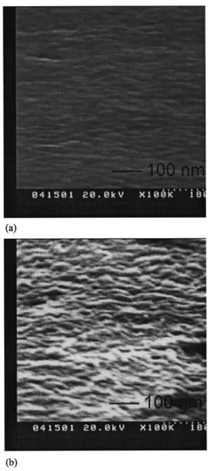
disap-pear. Moreover, from the sheet resistance data shown in Fig. 3, phase agglomeration in the Si0.86Ge0.14 sample occurred with a 1000 °C rapid thermal anneal. This is expected to worsen the surface roughness. The surface morphology seen in SEM micrographs for undoped Co/Si0.86Ge0.14samples an-nealed at 900 and 1000 °C is shown in Figs. 8共a兲 and 8共b兲, respectively. It can be seen that the surface becomes much
FIG. 5. XRD spectra of 17 nm Co deposited on the undoped 100 nm Si0.86Ge0.14layer after annealing at different temperatures for 30 s.
FIG. 6. 共a兲 XRD spectra of the Co(Si1⫺yGey)(310) phase for 17 nm Co
deposited on the 100 nm undoped Si0.86Ge0.14sample after different RTA
conditions, and共b兲 the diffraction angle of the Co(Si1⫺yGey) phase and the
relative CoGe ratio y after rapid thermal anneals at different temperatures for different samples.
rougher by increasing the RTA temperature from 900 to 1000 °C.
Figure 9 is a TEM micrograph of the B-doped Si0.86Ge0.14 sample after 900 °C RTA. Based on XRD analysis, only the CoSi2phase is found at this temperature, and it is represented by the large grain in the TEM micrograph. The underlying Si0.86Ge0.14layer is almost consumed and silicidation has ex-tended into the Si region. Furthermore, we can see very clearly that there are some small decorations around the CoSi2grain boundaries. It has been reported that the decora-tions are Ge-rich Si1⫺zGez(z⬎x) alloys.23,28 Si1⫺zGez
pre-cipitates segregate from the Co silicide region and become distributed mostly in the upper and bottom parts of the Co/Si1⫺xGexreacted region. These results confirm the trends
of the AES and SIMS profiles.
To elucidate the effects of the boron on silicide reaction and the lattice distortion at the underlying Si1⫺xGex layer,
we summarize below the important experimental results. At 500 °C, B accumulation is very near the surface. At 700 and 900 °C, boron atoms pile up at the upper Co/Si1⫺xGex
reac-tion layer, which is between the cobalt silicide and thin Co-rich surface layer. The same phenomenon can be observed from the interaction of Co with the B-doped Si sample at temperatures below 500 °C.22 The reason for the B pileup may be the low solubility of boron in crystalline Co silicides
(⬃5⫻1019cm⫺3). The boron atoms are pushed out of the Co/Si1⫺xGex or Co/Si silicide region. For the case of
con-ventional Co/Si, the boron atoms accumulate at the interface between CoSi and Co-rich layers after a low temperature anneal 共500 °C兲. After higher temperature annealing
共⬎500 °C兲, the Co-rich layer is consumed, so the boron
at-oms move to the surface region. For the Co/Si1⫺xGex case,
we assume that boron atoms segregate out of the monosili-cide layer and are injected along the silimonosili-cide grain boundaries or defects into the Ge-rich Si1⫺zGez precipitates, where the
solubility of boron is higher than it is in the silicide region. This assumption could explain the phenomenon that a B pileup still occurs at the upper silicide region in the Co/Si1⫺xGex sample even after high temperature annealing FIG. 7. High-resolution XRD spectra of Co共17 nm兲 deposited on 共a兲
un-doped and共b兲 B-doped Si0.86Ge0.14layers after annealing at different
tem-peratures for 30 s.
FIG. 8. SEM micrographs of the surface morphology of the undoped Co/Si0.86Ge0.14sample annealed for 30 s at共a兲 900 and 共b兲 1000 °C. After
1000 °C annealing, the surface is severely roughened, indicating the occur-rence of agglomeration.
1453 Huanget al.: Study of boron effects on the reaction of Co and Si1ÀxGex 1453
共700 and 900 °C兲. In addition, the reason why the boron
pileup region is very close to the Ge accumulation region can also be explained. According to the diffraction angle of the Co共Si1⫺yGey) 共210兲 phase, the CoGe fraction of the sum of
CoSi and CoGe, y, in the B-doped sample is indeed smaller than that in the undoped sample. This phenomenon may be explained by the fact that boron atoms tend to accumulate with Ge atoms. In other words, B atoms may grab Ge atoms to form B-doped Si1⫺zGez clusters as the Si and Ge atoms diffuse toward the Co film. This is consistent with the results of the AES profiles that more Ge atoms tend to accumulate at the upper Co/Si1⫺xGex reaction region in B-doped samples.
The other interesting effect is the reduced mobility of misfit dislocation for lattice distortion in the underlying B-doped Si1⫺xGex layer by B atoms. Relaxation is
accom-panied by the formation and extension of dislocations along which the Ge and Si atoms could outdiffuse. Recently it was reported that a small-sized atom such as C could decrease the occurrence of misfit dislocation in the Si1⫺xGex layer, and
therefore inhibit lattice relaxation.27 From our high resolu-tion XRD spectra, the lattice relaxaresolu-tion is indeed retarded by B atoms, similar to the effect of C atoms in the Si1⫺xGex
layer.
IV. CONCLUSION
In this article, a detailed comparison of the Co reaction with undoped and in situ boron-doped strained Si0.86Ge0.14 and Si0.91Ge0.09layers was made. Due to the low solubility of boron in the silicide film, boron atoms were found to segre-gate out of the silicide layer and were injected into the Ge-rich Si1⫺zGez precipitates at the upper silicide region. In
addition, more Ge atoms accumulated in the same region than the undoped sample. This means that boron pileup may cause the Ge-rich Si1⫺zGezprecipitates to accumulate in the
upper silicide region. In addition, Ge segregation to the up-per silicide region and to the monosilicide 共and disilicide兲 boundaries was also observed from AES and TEM analyses. Furthermore, with more Ge segregation from monosilicide, a smaller fraction, y, of CoGe was incorporated into the
Co共Si1⫺yGey) ternary phase, as seen by the XRD spectra of
the Co共Si1⫺yGey)(210) phase. Finally, we discovered for the
first time that the presence of boron atoms, similar to that of carbon ones, inhibited lattice relaxation of the underlying Si1⫺xGex layer. This inhibition of lattice relaxation was
probably because small atoms decrease the misfit dislocation mobility of the underlying Si1⫺xGexlayer.
ACKNOWLEDGMENTS
The authors would like to thank Dr. F. M. Pan, Dr. W. F. Wu, and Dr. H. C. Lin for experimental assistance. This work was supported in part by the National Science Council of the Republic of China共No. NSC88-2215-E009-048兲.
1X. Xiao, C. Sturm, S. R. Parihar, S. A. Lyon, D. Meyerhofer, S. Palfery,
and F. V. Shallcross, IEEE Electron Device Lett. EDL-14, 199共1993兲.
2G. L. Patton, J. H. Comfort, B. S. Meyerson, E. F. Crabbe, B. De Fresart,
J. M. C. Stork, J. Y. C. Sun, D. L. Harame, and J. M. Burgatz, IEEE Electron Device Lett. EDL-11, 171共1990兲.
3J. M. Stork, E. J. Prinz, and C. W. Magee, IEEE Electron Device Lett.
EDL-12, 303共1991兲.
4
P. M. Garone, V. Venkataraman, and J. C. Sturm, Tech. Dig. Int. Electron Devices Meet. 90共1990兲.
5H. Kanaya, F. Hasegawa, E. Yamaka, T. Moriyama, and M. Nakajima,
Jpn. J. Appl. Phys., Part 1 28, 544共1989兲.
6Q. Z. Hong and J. W. Mayer, J. Appl. Phys. 66, 611共1989兲. 7
H. K. Liou, X. Wu, and U. Gennser, Appl. Phys. Lett. 60, 577共1992兲.
8R. D. Thompson, K. N. Tu, J. Angillelo, S. Delage, and S. S. Iyer, J.
Electrochem. Soc. 135, 3161共1988兲.
9O. Thomas, F. M. D’Heurle, S. Delage, and G. Scilla, Appl. Surf. Sci. 38,
27共1989兲.
10
O. Thomas, F. M. D’Heurle, and S. Delage, J. Mater. Res. 5, 1453共1990兲.
11W.-J. Qi, B.-Z. Li, W.-N. Huang, and Z.-Q. Gu, J. Appl. Phys. 77, 1086
共1995兲.
12Z. Wang, Y. L. Chen, H. Ying, R. J. Nemanich, and D. E. Sayers, Mater.
Res. Soc. Symp. Proc. 320, 397共1994兲.
13
A. Buxbaum, M. Eizenberg, A. Raizman, and F. Scha¨ffler, Appl. Phys. Lett. 59, 665共1991兲.
14M. C. Ridgway, R. G. Elliman, N. Hauser, J.-M. Baribeau, and T. E.
Jackman, Mater. Res. Soc. Symp. Proc. 260, 857共1992兲.
15
F. Lin, G. Sarcona, M. K. Hatalis, A. F. Cserhati, E. Austin, and D. W. Greve, Thin Solid Films 250, 20共1994兲.
16M. Glu¨ck, A. Schuppen, M. Ro¨sler, W. Heinrich, J. Hersener, U. Ko¨nig,
O. Yam, C. Cytermann, and M. Eizenberg, Thin Solid Films 270, 549
共1995兲.
17
A. Appelbaum, R. V. Knoell, and S. P. Murarka, J. Appl. Phys. 57, 1880
共1985兲.
18G. Ottaviani, K. N. Tu, P. Psaras, and C. Nobili, J. Appl. Phys. 62, 2290
共1987兲.
19
S. P. Ashburn, M. C. O¨ ztu¨rk, G. Harris, and D. M. Maher, J. Appl. Phys.
74, 4455共1993兲.
20F. Wald and S. J. Michalik, J. Less-Common Met. 24, 277共1971兲. 21M. C. Ridgway, R. G. Elliman, R. Pascual, J. L. Whitton, and J.-M.
Baribeau, Mater. Res. Soc. Symp. Proc. 311, 155共1993兲.
22
C. Zaring, A. Pisch, J. Cardenas, P. Gas, and B. G. Svensson, J. Appl. Phys. 80, 2742共1996兲.
23C. Cytermann, E. Holzman, R. Brener, M. Fastow, M. Eizenberg, M.
Glu¨ck, H. Kibbel, and U. Ko¨nig, J. Appl. Phys. 83, 2019共1998兲.
24
L. P. Chen, C. T. Chou, G. W. Huang, and C. Y. Chang, Appl. Phys. Lett.
67, 3001共1995兲.
25P. L. Smith, C. M. Osburn, D. S. Wen, and G. McGuire, Mater. Res. Soc.
Symp. Proc. 160, 299共1990兲.
26W. M. Chen, S. Pozder, Y. Limb, A. R. Sitaram, and B. Fiordalice, Mater.
Res. Soc. Symp. Proc. 429, 163共1996兲.
27A. Eyal, R. Brener, R. Beserman, M. Eizenberg, Z. Atzmon, D. J. Smith,
and J. W. Mayer, Appl. Phys. Lett. 69, 64共1996兲.
28Z. Wang, D. B. Aldrich, Y. L. Chen, D. E. Sayers, and R. J. Nemanich,
Thin Solid Films 270, 555共1995兲. FIG. 9. Cross-sectional TEM micrograph of the B-doped Si0.86Ge0.14sample