Studies on Ferroelectric Properties of Sol-Gel Derived
Pb
„Zr
0.53Ti
0.47…O
3Using Ba
0.5Sr
0.5RuO
3as the Conductive Electrodes
Y. K. Wang,aC. H. Huang,aT. Y. Tseng,a,zand Pang Linb
aDepartment of Electronics Engineering and Institute of Electronics, andbInstitute of Materials Science and Engineering, National Chiao Tung University, Hsinchu 30050, Taiwan
Pb共Zr0.53Ti0.47)O3共PZT兲 thin films with a 共110兲 preferred orientation were prepared on Ba0.5Sr0.5RuO3(BSR兲/Ru/SiO2/Si sub-strates using a sol-gel method. The oxide bottom electrode, BSR, was fabricated at various temperatures on Ru/SiO2/Si substrates by rf sputtering. The annealed PZT films on BSR/Ru/SiO2/Si substrates exhibited improved crystallinity. The electrical properties of PZT films, such as the electric field共E兲 induced variations of the leakage current density, the dielectric constant, and the polarization were strongly dependent on the processing temperatures of the PZT films as well as the bottom oxide electrode. A typical PZT thin film annealed at 650°C on the BSR electrode, which was deposited at 450°C on the Ru/SiO2/Si substrate by a sputtering technique, has a leakage current of 2.7⫻ 10⫺7A/cm2at an applied electric field of 500 kV/cm and a dielectric constant of 968. From the polarization-electric field characteristics, the remanent polarization and coercive field of the PZT were found to be 38.9C/cm2and 59.6 kV/cm, respectively, at an applied voltage of 5 V. The PZT films exhibited fatigue-free characteristics up to⬃1.0 ⫻ 1012switching cycles under 5 V bipolar pulses.
© 2004 The Electrochemical Society. 关DOI: 10.1149/1.1667522兴 All rights reserved.
Manuscript submitted January 23, 2003; revised manuscript received October 29, 2003. Available electronically March 3, 2004.
Pb共Zr,Ti兲O3共PZT兲 thin films have attracted attention because of the excellent ferroelectric properties, which can be exploited for applications in nonvolatile random access memories 共NVRAMs兲 and dynamic random access memories共DRAMs兲.1-4However, many reports have indicated that the PZT thin films have serious fatigue problems when deposited on metal electrodes because of the degra-dation of the film/electrode interface, which results in a relatively shorter number of switching cycles.5-7The conductive metallic ox-ide electrodes, such as RuO2,8IrO2,9(La0.5,Sr0.5)CoO3,10BaRuO3 共BRO兲,11SrRuO
3共SRO兲,12and BaxSr1⫺xRuO3共BSR兲,13have been found to improve the fatigue properties of the PZT capacitors. The polarization fatigue, which arises out of repeated switching cycles, gets suppressed at a ferroelectric film/oxide electrode heterostruc-ture as the oxide electrodes act as sinks for the oxygen vacancies. The selection of electrode materials will also affect the microstruc-ture and the electrical properties of the thin films. Moreover, the perovskite oxide electrodes should have similar lattice parameter and crystal structure with PZT thin films as these characteristics decide the formation of the chemically and thermally stable PZT/ perovskite oxide electrode interface, which eventually enhance the ferroelectric characteristics of PZT films.14However, it is very difficult to deposit preferentially oriented PZT or BSR films on silicon substrates. In most of the studies on epitaxial PZT or BSR thin films, the films were deposited on SrTiO3 共STO兲 or LaAlO3 共LAO兲 substrates.15-17 In our earlier study,18 the 共110兲-oriented SRO oxide electrodes were deposited on an Ru/SiO2/Si substrate at a low temperature, subsequently 共110兲-oriented PZTs were grown on SRO(110)/Ru/SiO2/Si substrates. The PZT films on SRO(110)/Ru/SiO2/Si exhibited improved ferroelectric properties. Obviously, the enhancement in the ferroelectric properties of PZT deposited on the perovskite oxide electrodes can be obtained and would be of interest for future ferroelectric memory applications. However, in our previous study, a detailed investigation of structure and ferroelectric properties was not carried out. In this study, we prepared highly oriented共110兲 PZT thin films on conducting oxides, namely (Bs,Sr兲RuO3 共BSR兲, as bottom electrodes. Thin films of BSR with 共110兲 preferred orientation were sputter-deposited on Ru/SiO2/Si substrates. The structure and the ferroelectric properties of PZT films were studied in detail.
Experimental
The initial attempt to prepare the BSR target through a solid-state reaction using stoichiometric amounts of a RuO2, SrCO3, and BaCO3mixture as the starting materials was not successful. Subse-quently, BaRuO3 and SrRuO3 were prepared separately through a solid-state reaction using BaCO3, SrCO3, and RuO2as starting ma-terials and then mixed and different ratios of the end members used to form the BSR solid solution were calcined. The experimental conditions employed for the synthesis of BRO and SRO phases can be summarized as follows: stoichiometric amounts of RuO2 and BaCO3were mixed in a ball mill and calcined at 1000°C for 4 h to from single-phase BaRuO3 共BRO兲 powder. Similarly, the single-phase SrRuO3 was prepared from high purity RuO2 and SrCO3 powders by calcining the well-mixed reactant mixture for 4 h at 1250°C. The phase formations of both end members were confirmed by X-ray diffraction共XRD兲. In order to prepare the solid-solution target, BSR, with the desired composition, Ba0.5Sr0.5RuO3, the sto-ichiometric amounts of BRO and SRO were mixed in a ball mill followed by calcination at 1500°C. However, the XRD characteriza-tion of the 1500°C calcined powder did not confirm the formacharacteriza-tion of the BSR phase. Finally, the BSR target was fabricated by mixing different ratios of well-crystallized BRO and SRO phases. In our experiments, we used the low-temperature calcined 共600°C, 4 h兲 mixture of BRO and SRO powders as the target material. Based on XRD results共not shown here兲, such a 600°C calcined powder target is the mixture of BRO and SRO phases.
The BSR thin films were deposited on Ru/SiO2/Si(100) sub-strates at various temperatures by rf magnetron sputtering. The ther-mally oxidized silicon dioxide layer (SiO2, 100 nm thick兲 was em-ployed to suppress the reaction between Ru and silicon. The 50 nm thick Ru metal films were deposited at 400°C using rf sputtering. The deposition conditions and the resultant thicknesses of Ru and BSR films are listed in Table I. The PZT films with a thickness of 200 nm were grown by a sol-gel method. The annealing of the films was performed in a tube furnace at various temperatures ranging from 500 to 700°C under O2atmosphere. The BSR top electrodes with an area of 4.9⫻ 10⫺5cm2were sputter deposited onto the PZT films at room temperature, and then thermally treated at 400°C for 10 min to reduce the interface defects during sputtering. The crys-tallinity of the films was examined by XRD共Siemens D5000兲, with Cu K␣ radiation. The surface morphology and the microstructure were observed by using atomic force microscope 共AFM, Digital Instruments Nanoscope III兲 and scanning electron microscope
共SEM, Hitachi S-4700兲, respectively. The capacitance-voltage 共C-V兲 characteristics were measured with an impedance-gain-phase ana-lyzer共Hewlett-Packard, HP, 4194A兲 at 100 kHz. The current-voltage (I-V) measurements were performed by using a semiconductor pa-rameter analyzer 共HP4156B兲. The ferroelectric properties of the films were measured using a RT66A ferroelectric tester 共Radiant Technologies, Inc.兲.
Results and Discussion
Figure 1 shows the XRD patterns of BSR films deposited on Ru/SiO2/Si substrates at various temperatures. The deposited BSR films have a preferred共110兲 orientation with the well-defined peaks appearing at deposition temperatures as low as 300°C, and the peak intensity of 共110兲-oriented BSR films increases with increasing deposition temperature. Similar results were observed when the SRO was deposited on Ru/SiO2/Si substrates.18We also observed the共110兲 peak of the RuO2phase for the films deposited at 450°C due to the oxidation reaction at the interface between BSR and Ru at high deposition temperature. The additional peak corresponding to Ru共100兲 appears at deposition temperatures in the range from 450 to 500°C.
The XRD patterns of the PZT films deposited on BSR共450°C deposited兲/Ru/SiO2/Si substrates and annealed at temperatures ranging from 400 to 700°C are shown in Fig. 2. A strong 共110兲 preferred orientation appeared in PZT films annealed at 450°C, and this preferred orientation is further enhanced by increasing the an-nealing temperature up to 700°C. We observed from our XRD
re-sults, that the PZT-共110兲 films crystallized on the 300°C deposited BSR electrodes. The 共110兲-oriented BSR bottom electrode could enhance the crystallization of PZT films to form the preferred ori-entation of共110兲. In addition, all of the XRD patterns of PZT films annealed at high temperature could find the 共110兲 orientation of RuO2even though the bottom electrode was deposited at lower than 450°C. The XRD patterns of the BSR films, which were deposited on Ru/SiO2/Si substrates at various temperatures and then furnace annealed at 600°C in O2, that is, the same heat-treatment with PZT
Figure 1. XRD patterns of BSR films deposited on Ru/SiO2/Si substrates at the various temperatures indicated.
Figure 2. XRD patterns of PZT films deposited on 450°C-grown BSR/Ru/SiO2/Si substrates and annealed at the various temperatures indi-cated.
Figure 3. XRD patterns of BSR films deposited on Ru/SiO2/Si substrates at the various temperatures indicated and then furnace-annealed at 600°C under O2atmosphere.
Table I. The deposition conditions and thicknesses of Ru and BSR films.
Films Ru BSR
Target Metallic Ru SRO and BRO
packed powder
Substrate temperature 400°C 300-500°C, room temperature
Sputtering gas Ar Ar/O2⫽ 3/1
RF power共W兲 100 100
Working pressure共mTorr兲 10 10
films, are indicated in Fig. 3. It appears the RuO2(110) and the Ru共100兲 peaks in addition to the BSR共110兲 and the Ru共002兲 peaks. The formation of RuO2 is attributed to the interface reaction be-tween Ru and BSR leading to oxidation of the Ru at high annealing temperatures. The RuO2(110) and the Ru共100兲 formation would not affect the crystallization of the PZT films, because the BSR crystal-lization directly influenced the PZT thin-film growth.
The dielectric constant and the loss tangent of the PZT films as a function of the annealing temperature and BSR electrode deposition temperature are depicted in Fig. 4. The dielectric constant and the loss tangent increase with the increase in annealing temperature of the PZT films and deposition temperature of the BSR bottom elec-trodes. When the annealing temperature is lower than 450°C, the dielectric constants of the PZT films are small because they are amorphous. When the annealing temperature is higher than 450°C, the PZT films are well crystallized and have high dielectric con-stants. The high dielectric constant for the high-temperature an-nealed PZT films is attributed to better crystallinity, larger grain size,
and higher polarization of the highly oriented films. The evidence of high annealing temperature enhancement of the grain growth of the PZT films is shown in Fig. 5. On the other hand, the better crystal-lization of the BSR bottom electrodes could enhance the crystalliza-tion of the PZT films and consequently increase their dielectric con-stants. Figure 6 shows the leakage current density of the PZT films deposited on BSR 共450°C deposited兲/Ru/SiO2/Si substrates. The symmetry of the curves indicates the same structure and material for both the top and the bottom electrodes. The leakage current density of the PZT film annealed at 400°C has a low value of 5⫻ 10⫺10 A/cm2at 750 kV/cm because of its amorphous nature, whereas the 700°C-annealed PZT has a high leakage current of 1.3⫻ 10⫺6 A/cm2at the same electric field. The leakage current increases with elevated annealing temperature, because the column grains are eas-ily grown in the PZT films at high temperatures 共Fig. 7兲, which supply short-circuit paths under the applied bias. The interface reac-Figure 4. Dielectric constant and loss tangent of PZT thin films annealed at
various temperatures on the BSR bottom electrodes deposited at various temperatures.
Figure 5. SEM images of PZT films deposited on the 450°C-grown BSR/Ru/SiO2/Si substrates annealed at共a兲 600, 共b兲 650, 共c兲 700, and 共d兲 750°C.
Figure 6. The I-V characteristics of PZT thin films deposited on the 450°C-grown BSR/Ru/SiO2/Si substrates and annealed at the various temperatures indicated.
Figure 7. SEM cross section of the PZT film deposited on the 450°C grown BSR/Ru/SiO2/Si substrate and annealed at 700°C.
tions between BSR and PZT films might also deteriorate the PZT performance. In addition, lead loss easily occurs in the high anneal-ing temperatures, which might induce the increase of the leakage current and the loss tangent. The deposition temperature of the BSR electrodes also affects the leakage current of the PZT thin films. The better crystallized BSR electrode would lead to the PZT films hav-ing a larger column grain size, which is the main cause for the larger leakage current.
The polarization-electric field hysteresis loops for the PZT films on the 450°C-deposited BSR electrodes, which were annealed at various temperatures, are illustrated in Fig. 8. The remanent
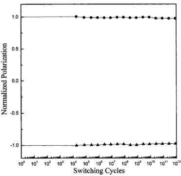
polar-ization ( Pr) of PZT films increases with an increase in annealing temperature up to 650°C, as a result of better crystallization of the PZT films. The 650°C-annealed PZT films have a relatively high value of Pr, 38.9C/cm2. The Prof the 700°C annealed PZT films were lower than that of the 650°C-annealed-PZT, which may be due to the interfacial reaction between oxide and electrode. To verify this point, the secondary ion mass spectroscopy共SIMS兲 analysis of the interface of the PZT/BSR heterostructure was carried out, and its result is indicated in Fig. 9. The interdiffusion between PZT film and the BSR electrode indeed occurred at the high temperature of 700°C, which results in a reduction of Prvalues. We also attempted to deposit a thin CeO2 共15 nm兲 between the 700°C-annealed-PZT film and the bottom electrode and then measure its hysteresis loop. The result in Fig. 10 indicates that the Pr, 38.2C/cm2of 700°C-annealed PZT films using the CeO2 buffer layer is larger than 36.1 C/cm2 without the CeO2 layer. Obviously, the CeO2 provides a diffusion barrier to reduce ferroelectric and oxide bottom electrode interdiffusion. Some studies reported that the strontium atoms dif-fused into ferroelectric films easily, which degrades the ferroelectric properties.19It is supposed that strontium and barium ions diffused into PZT共Fig. 9兲 have been obstructed the by CeO2 buffer layer, resulting in higher Prof the PZT film. The Prvalues of the annealed PZT films on various temperature-deposited BSR electrodes are summarized in Table II. The fatigue characteristics of the 650°C-annealed-PZT films are depicted in Fig. 11, which indicates that the Figure 8. Polarization vs. electric field characteristics of PZT thin films
deposited on a 450°C BSR bottom electrode and annealed at various tem-peratures.
Figure 9. The SIMS analysis of the PZT thin film on the 450°C-deposited BSR bottom electrode and then annealed at 700°C.
Figure 10. Polarization vs. electric field characteristic of the PZT thin film deposited on CeO2共15 nm兲/BSR/SiO2/Si substrate and annealed at 700°C.
Table II. The remanent polarization values of various temperature-annealed PZT films deposited on various tempera-ture prepared BSR electrodes.
Remanent polarization
共 C/cm2兲
Ba0.5Sr0.5RuO3deposition temperature共°C兲
300 350 400 450 500 PZT annealing temperature共°C兲 500 10.8 15.8 19.2 24.4 28.8 550 15.5 23.3 26.0 30.5 33.5 600 18.1 29.3 32.8 33.8 38.5 650 21.7 32.5 35.6 38.9 43.5 700 23.9 28.8 32.6 36.1 41.2
highly共110兲 oriented PZT films deposited on BSR/Ru/SiO2/Si sub-strates do not show any deterioration after⬃1012switching cycles.
Conclusions
We have demonstrated the deposition and the characterization of the PZT thin films with a共110兲-preferred orientation on BSR bottom electrodes by a sol-gel method. The bottom electrode, BSR, was deposited by rf sputtering on Ru/SiO2/Si substrates. A low leakage current has been recorded for the PZT films annealed at lower tem-peratures. However, the leakage current increased for the films
an-nealed at higher temperatures. The value of the dielectric constant and the Prwere also increased with raising the annealing tempera-ture up to 650°C. However, the Pr value decreased on further in-creasing the annealing temperature, which was attributed to stron-tium and barium ions diffused into PZT films. The PZT films were fatigue-free even after⬃1012switching cycles.
Acknowledgment
This work was supported by the National Science Council R. O. C. under contract no. NSC 91-2219-E-009-028.
National Chiao Tung University assisted in meeting the publication costs of this article.
References
1. J. T. Evans, Jr. and R. Womack, IEEE J. Solid-State Circuits, 23, 1171共1998兲. 2. W. A. Geideman, IEEE Trans. Ultrason. Ferroelectr. Freq. Control, 38, 704共1991兲. 3. J. F. Scott and C. A. Paz de Araujo, Science, 246, 1400共1989兲.
4. T. Y. Tseng, in Proceedings of International Electron Devices and Materials Sym-posia, Hsinchu, Taiwan, 2-5, 89共1996兲.
5. K. R. Bellur, H. N. Al-Shareef, S. H. Rou, K. D. Gifford, O. Auciello, and A. I. Kingon, in Proceedings of the 8th IEEE International Symposium on the Applica-tions of Ferroelectrics, 448共1992兲.
6. H. M. Duiker, P. D. Beale, J. F. Scott, C. A. Paz de Araujo, B. M. Melnick, J. D. Cuchiaro, and L. D. McMillan, J. Appl. Phys., 68, 5783共1990兲.
7. P. K. Larsen, G. J. M. Dormans, D. J. Taylor, and P. J. van Veldhoven, J. Appl. Phys., 76, 2405共1994兲.
8. G. J. Norga, D. J. Wouters, A. Bartic, Laura Fe`, and H. E. Maes, in Proceedings of the 11th IEEE International Symposium on Applications of Ferroelectrics, 3-6 共1998兲.
9. T. Nakamura, Y. Nakao, A. Kamisawa, and H. Takasu, Jpn. J. Appl. Phys., Part 1, 33, 5207共1994兲.
10. R. Ramesh, T. Sands, and V. G. Keramidas, J. Electron. Mater., 23, 19共1994兲. 11. S.-M. Koo, L.-R. Zheng, and K. V. Rao, J. Electron. Mater., 14, 3833共1999兲. 12. C. Guerrero, J. Rolda´n, C. Ferrater, M. V. Garcia-Cuenca, F. Sa´nchez, and M.
Varela, Solid-State Electron., 45, 1433共2001兲.
13. D.-K. Choi, B.-S. Kim, S.-Y. Son, S.-H. Oh, and K.-W. Park, J. Appl. Phys., 86, 3347共1999兲.
14. K. P. Jayadevan and T. Y. Tseng, J. Mater. Sci.: Mater. Electron., 13, 439共2002兲. 15. J. H. Kim, A. T. Chien, F. F. Lange, and L. Wills, J. Mater. Res., 14, 1190共1999兲. 16. C. M. Foster, G. R. Bai, R. Csencsits, J. Vetrone, R. Jammy, L. A. Wills, E. Carr,
and J. Amano, J. Appl. Phys., 81, 2349共1997兲.
17. K. Nagashima, M. Aratani, and H. Funahubo, J. Appl. Phys., 89, 4517共2001兲. 18. Y. K. Wang, T. Y. Tseng, and P. Lin, Appl. Phys. Lett., 80, 3790共2002兲. 19. S.-M. Yoon, E. Tokumitsu, and H. Ishiwara, Appl. Surf. Sci., 117Õ118, 447 共1997兲.
Figure 11. Fatigue behavior of the 650°C-annealed PZT thin film which was deposited at 450°C on BSR/Ru/SiO2/Si with a 100 kHz bipolar square wave peak-to-peak fatigue voltage of 10 V.