1394 IEEE ELECTRON DEVICE LETTERS, VOL. 32, NO. 10, OCTOBER 2011
Effect of Lateral Body Terminal on
Silicon–Oxide–Nitride–Oxide–Silicon
Thin-Film Transistors
Hung-Wei Li, Ting-Chang Chang, Geng-Wei Chang, Chia-Sheng Lin, Tsung-Ming Tsai,
Fu-Yen Jian, Ya-Hsiang Tai, and Ming-Hsien Lee
Abstract—We investigate lateral-body-terminal silicon–oxide–
nitride–oxide–silicon thin-film transistors (LBT SONOS TFTs) under erasing operation. These devices have superior erasing efficiency by gate as well as lateral body electrode exerting bias. The erasing mechanism of LBT SONOS TFTs has been illustrated by the energy band diagrams. Holes gain sufficient energy by the electric field in the deep-depletion region to surmount the tun-neling oxide barrier because of exerting body bias under erasing operation. In addition, the lateral body terminal exerting bias can enhance the erasing efficiency and is confirmed by different erasing conditions and structures. In addition, to verify the hole current injecting from the lateral body site, the size effect of LBT SONOS TFTs is also discussed.
Index Terms—Erasing efficiency, hole injection, silicon–oxide–
nitride–oxide–silicon (SONOS), thin-film transistors (TFTs).
I. INTRODUCTION
L
OW-TEMPERATURE polysilicon (LTPS) thin-film tran-sistors (TFTs) have been adopted in flat-panel displays, in-cluding active-matrix liquid-crystal displays and active-matrix organic light-emitting diode displays [1]. The major advantage of LTPS TFTs is its suitability for multifunctional active-matrix displays because it can integrate sensor, controller [2], Manuscript receivedJune 21, 2011; revised July 7, 2011; accepted July 12, 2011. Date of publication August 17, 2011; date of current version September 28, 2011. This work was supported by the National Science Council of Taiwan under Contracts NSC99-2120-M-110-001, NSC97-2112-M-110-009-MY3, and NSC 99-2221-E-009-121. The review of this letter was arranged by Editor W. Wong.H.-W. Li and G.-W. Chang are with the Department of Photonics and the Institute of Electro-Optical Engineering, National Chiao Tung University, Hsinchu 300, Taiwan (e-mail: [email protected]; b922030049@ gmail.com).
T.-C. Chang and C.-S. Lin are with the Department of Physics and the Center for Nanoscience and Nanotechnology, National Sun Yat-Sen Uni-versity, Kaohsiung 804, Taiwan (e-mail: [email protected]; [email protected]).
T.-M. Tsai is with the Institute of Materials Science and Engineering, National Sun Yat-Sen University, Kaohsiung 804, Taiwan (e-mail: tmtsai@ faculty.nsysu.edu.tw).
F.-Y. Jian is with the Department of Physics and the Center for Nanoscience and Nanotechnology, National Sun Yat-Sen University, Kaohsiung 804, Taiwan, and also with the Institute of Electronics, National Chiao Tung Uni-versity, Hsinchu 300, Taiwan (e-mail: [email protected]).
Y.-H. Tai is with the Department of Photonics and the Display Institute, National Chiao Tung University, Hsinchu 30010, Taiwan (e-mail: yhtai@ mail.nctu.tw).
M.-H. Lee is with the Advanced Process Department, AU Optronics Corpo-ration, Hsinchu 300, Taiwan (e-mail: [email protected]).
Color versions of one or more of the figures in this letter are available online at http://ieeexplore.ieee.org.
Digital Object Identifier 10.1109/LED.2011.2162481
Fig. 1. (a) Schematic cross-sectional view of SONOS TFTs with LBT. (b) Electrical characteristics under the erasing condition with both VG=
−12 V and VB= 10 V.
and memory [3] into a panel for system-on-panel (SOP) ap-plications. Silicon–oxide–nitride–oxide–silicon (SONOS)-type TFTs serving as nonvolatile memory by embedding a trapping layer into the gate oxide of the transistor have been proposed for SOP applications because their processes are simple and fully compatible with the poly-Si TFT process [4]–[8]. The read principle of the SONOS memory device is by measuring the corresponding current between the programming and erasing states and identifying the distinct status of the memory device [9], [10]. Thus, the memory window, i.e., the threshold-voltage difference between the programming and erasing states, must be large enough to distinguish the status of the memory device. However, traditional SONOS TFTs have poor erasing effi-ciency. Hole tunneling is forbidden due to the large hole barrier height (> 4 eV) of the oxide, so that the memory window cannot be distinguished clearly [11], [12]. Therefore, a variety of approaches to enhance the erasing efficiency is worthy of study. In this letter, lateral body terminal (LBT) SONOS TFTs are used to enhance the erasing efficiency. These devices have superior erasing efficiency than conventional three-terminal SONOS memory devices. In addition, to confirm the erasing hole current injecting from the lateral body site, we investigate the size effect of LBT SONOS TFTs under erasing operation and explain it with the schematic.
II. EXPERIMENTALSETUP
Fig. 1(a) shows the schematic cross-sectional view of a SONOS-TFT with LBT. The devices used in this letter are n-channel SONOS TFTs with top gate and self-aligned lightly doped drain (LDD) structures fabricated on a Corning 1737 glass substrate. The detailed fabrication procedures are as 0741-3106/$26.00 © 2011 IEEE
LI et al.: EFFECT OF LBT ON SILICON–OXIDE–NITRIDE–OXIDE–SILICON THIN-FILM TRANSISTORS 1395
follows. First, a silicon oxide buffer layer and a 50-nm-thick undoped amorphous-Si (a-Si) film were deposited sequen-tially by plasma-enhanced chemical vapor deposition (PECVD) at 380 ◦C. Then, the polysilicon channel was formed by a 308-nm XeCl excimer laser with a line-shaped beam power of 350 mJ/cm2, and a 95% laser overlap ratio was adopted to obtain large grain size and better uniformity of the active layer. The source/drain and LDD region were formed by the mass-separated ion implanter technique. Doping activation was performed at 530◦C/1-h thermal furnace. Next, the multilayer gate dielectric consisting of tunneling oxide (10 nm)/silicon nitride (20 nm)/top oxide (40 nm) (O/N/O) was deposited by PECVD. Then, MoW was sputtered and patterned as a gate metal. The fabrication process of the LBT SONOS-TFT was almost the same as that of the n-channel LTPS SONOS TFT. The p-doped LBT was the only difference. The fabrication pro-cess of LBT SONOS TFTs does not need any additional mask step. The body terminal was formed by the mass-separated ion implanter technique, just like the boron doping process of the conventional poly-Si TFT to form the P+ doping region. The electrical properties of SONOS TFTs with an LDD length of 1 μm were analyzed by using an Agilent B1500A semicon-ductor device analyzer. Here, the normalized drain current is defined as drain current/(width/length), i.e., ID/(W/L). The
threshold voltage is defined as the voltage, while N IDreaches
10−8A. All the measurements were taken at 30◦C. III. RESULTS ANDDISCUSSION
Fig. 1(b) shows the normalized current–voltage (I–V ) char-acteristics of the LBT SONOS TFT with W/L = 12/6 μm un-der erasing operation. Before the erasing operation, the memory device was programmed by a gate bias of 35 V for 1 s. Thus, electrons were injected from the channel through the tunnel oxide to the nitride layer by Fowler–Nordheim (FN) tunneling because the gate bias induced a high electric field. Then, the device was operating under erasing at a gate bias of−12 V as well as a body bias of 10 V for 1 s. The memory window can attain a threshold-voltage shift of 3.3 V under an erasing VGB of−22 V.
The memory window characteristics of SONOS TFTs at dif-ferent erasing conditions and structures are shown in Fig. 2(a). The memory window reaches 5.6 V under the LBT SONOS TFT at a gate bias of−16 V as well as a body bias of 10 V for 1 s. However, for the device after the erasing operation at a gate bias of −25 V without body bias, the memory window only reaches 0.55 V of threshold-voltage shift. In addition, compared with traditional three-terminal SONOS TFTs, the erasing efficiency is similar to that of the LBT SONOS TFT under erasing operation without body bias but is significantly poorer than that with body bias. The energy band diagram of the LBT SONOS TFT under erasing operation, as shown in Fig. 2(b), is used to illustrate the better erasing efficiency of LBT SONOS TFTs. Under erasing operation, the energy band of the gate region is raised when the gate exerts a negative bias. In addition, the LBT exerts a positive bias that can enhance hole injection to the channel from the lateral body site. Holes obtain kinetic energy by the electric field in the deep depletion of the
Fig. 2. (a) Memory window characteristics of SONOS TFTs at different erasing conditions and structures. (b) Band diagram at the erasing operation.
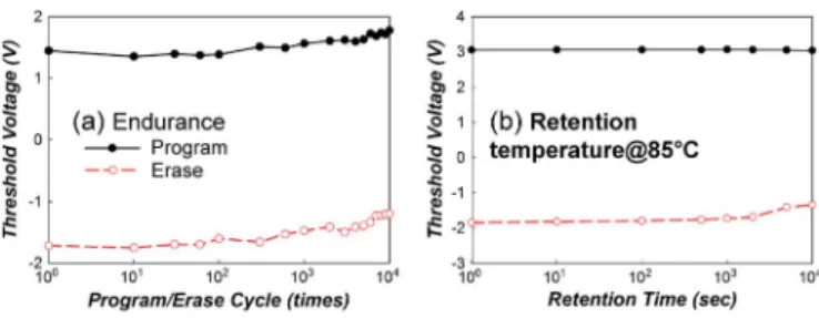
Fig. 3. (a) Endurance characteristics of LBT SONOS TFTs after various numbers of P/E cycles. (b) Retention characteristics of LBT SONOS TFTs measured after various periods, as the devices were heated at 85◦C.
channel region. Some holes gain sufficient energy to surmount the tunneling oxide barrier. Then, these holes are injected into the gate stack and are subsequently trapped in the charge-storage nitride layer to perform the erasing operation. However, traditional SONOS TFTs have poor erasing efficiency. Injecting holes to the nitride layer by FN tunneling becomes difficult because hole tunneling is forbidden due to the large hole barrier height (> 4 eV) of the oxide [11]. Therefore, LBT SONOS TFTs have better erasing efficiency than conventional devices. Fig. 3(a) shows the endurance characteristics of LBT SONOS TFTs following various numbers of program/erase (P/E) cycles. A memory window of 2.5 V is sufficiently large to identify digital states (0 or 1) in a logic memory circuit. The LBT SONOS memory device maintains a wide threshold-voltage window even after 104P/E cycles. In Fig. 3(b), the threshold-voltage shift of LBT SONOS TFTs was measured after various periods, as the devices were maintained at 85◦C. LBT SONOS TFTs exhibit good retention for 104 s, without a significant decline in the memory window.
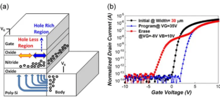
Moreover, the subthreshold slope appears to change under erasing operation, as shown as in Fig. 1(b), because holes are not uniformly injected into the storage layer. Fig. 4(a) shows the schematic of LBT SONOS TFTs under erasing operation. Most of the holes are injected into the storage layer edge near the lateral body site because they come from the LBT. Thus, this region, called the edge transistor, has a lower threshold voltage. The other region, called the main transistor, has a higher threshold voltage due to the smaller amount of holes injected into the storage layer. The side that is farther away from the lateral body has less hole injection. Therefore, the transfer
1396 IEEE ELECTRON DEVICE LETTERS, VOL. 32, NO. 10, OCTOBER 2011
Fig. 4. (a) Regions corresponding to the hole-rich region (the main transistor) and the hole-less region (the edge transistor) are illustrated. (b) Electrical characteristics of the LBT SONOS memory device with width = 30 μm. The erase conditions was VG=−8 V and VB= 10 V.
characteristics are determined by the parallel main transistor and edge transistor.
To confirm the erasing hole current injecting from the lateral body site, the size effect of LBT SONOS TFTs under erasing operation was discussed. The electrical characteristics of LBT SONOS TFTs with width = 30 μm are shown in Fig. 4(b). It is found that a hump appears at a certain drain current level around 8× 10⁻⁸A. It suggested that the hump curve is determined by the main transistor and the edge transistor. The main transistor means the upper part of the transfer characteristic which does not shift under erasing operation. The lower part of the Id–Vg curve, determined by the edge transistor, shifts toward the negative direction significantly after erasing. It indicates that holes are not uniformly injected into the storage layer. Most of the holes are injected near the lateral body side. The side that is farther away from the lateral body has less hole injection. Therefore, in the process of erasing, the hump phenomenon appears at the large width of LBT SONOS TFTs.
IV. CONCLUSION
In this letter, we have investigated LBT SONOS TFTs under erasing operation. These devices have superior erasing efficiency, and the erasing mechanism has been illustrated by the energy band diagrams. The role of the LBT under erasing operation has been verified by different erasing conditions and structures. In addition, the hump phenomenon presenting at the large width of LBT SONOS TFTs after erasing operation has also been discussed and explained with the schematic diagram.
ACKNOWLEDGMENT
This work was performed at the National Science Coun-cil Core FaCoun-cilities Laboratory for Science and Nano-Technology in the Kaohsiung–Pingtung area.
REFERENCES
[1] T. C. Lu, H. W. Zan, and M. D. Ker, “Temperature coefficient of poly-silicon TFT and its application on voltage reference circuit with tem-perature compensation in LTPS process,” IEEE Trans. Electron Devices, vol. 55, no. 10, pp. 2583–2589, Oct. 2008.
[2] K. Yoneda, R. Yokoyama, and T. Yamada, “Development trend of LTPS TFT LCDs for mobile applications,” in VLSI Symp. Tech. Dig., 2001, pp. 85–90.
[3] H. Tokioka, M. Agari, M. Inoue, T. Yamamoto, H. Murai, and H. Nagata, “Low power consumption TFT-LCD with dynamic memory embedded in pixels,” in Proc. SID, 2001, pp. 280–283.
[4] G. W. Chang, T. C. Chang, Y. E. Syu, Y. H. Tai, and F. Y. Jian, “On-current decrease after erasing operation in the nonvolatile memory device with LDD structure,” IEEE Electron Device Lett., vol. 32, no. 8, pp. 1038– 1040, Aug. 2011.
[5] A. J. Walker, S. Nallamothu, E.-H. Chen, M. Mahajani, S. B. Herner, M. Clark, J. M. Cleeves, S. V. Dunton, V. L. Eckert, J. Gu, S. Hu, J. Knall, M. Konevecki, C. Petti, S. Radigan, U. Raghuram, J. Vienna, and M. A. Vyvoda, “3-D TFT-SONOS memory cell for ultra-high density file storage applications,” in VLSI Symp. Tech. Dig., 2008, vol. 29. [6] A. J. Walker, “Sub-50 nm DG-TFT-SONOS—The ideal flash memory for
monolithic 3-D integration,” in Proc. Tech. Dig.—Int. Electron Devices
Meeting, 2008, vol. 1, pp. 1–4.
[7] S. C. Chen, T. C. Chang, P. T. Liu, Y. C. Wu, P. H. Yeh, C. F. Weng, S. M. Sze, C. Y. Chang, and C. H. Lien, “Nonvolatile polycrystalline silicon thin-film-transistor memory with oxide/nitride/oxide stack gate dielectrics and nanowire channels,” Appl. Phys. Lett., vol. 90, no. 12, pp. 122111-1–122111-3, Mar. 2007.
[8] Y. H. Lin, C. H. Chien, T. H. Chou, T. S. Chao, and T.-F. Lei, “Low-temperature polycrystalline silicon thin-film flash memory with hafnium silicate,” IEEE Trans. Electron Devices, vol. 54, no. 3, pp. 531–536, Mar. 2007.
[9] T. C. Chen, T. C. Chang, F. Y. Jian, S. C. Chen, C. S. Lin, M. H. Lee, J. S. Chen, and C. C. Shih, “Improvement of memory state misidenti-fication caused by trap-assisted GIDL current in a SONOS-TFT mem-ory device,” IEEE Electron Device Lett., vol. 30, no. 8, pp. 834–836, Aug. 2009.
[10] F. Y. Jian, T. C. Chang, A. K. Chu, S. C. Chen, T. C. Chen, Y. E. Hsu, H. C. Tseng, C. S. Lin, T. F. Young, and Y. L. Yang, “A 2 bit nonvolatile memory device with a transistor switch function accomplished with edge-FN tunneling operation,” Electrochem. Solid-State Lett., vol. 13, no. 5, pp. H166–H168, Mar. 2010.
[11] T. H. Hsu, H. T. Lue, Y. C. King, J. Y. Hsieh, E. K. Lai, K. Y. Hsieh, R. Liu, and C. Y. Lu, “A high-performance body-tied FinFET bandgap engineered SONOS (BE-SONOS) forNAND-type flash mem-ory,” IEEE Electron Device Lett., vol. 28, no. 5, pp. 443–445, May 2007.
[12] M. H. White, D. A. Adams, and J. Bu, “On the go with SONOS,” IEEE