Stability and mechanism of selective etching of ultrathin Ge films on the Si
„100… surface
upon chlorine adsorption
Juh-Li Wu, Shiang-Yuang Pan, and Deng-Sung Lin*
Institute of Physics, National Chiao-Tung University, 1001 Ta-Hsueh Road, Hsinchu 300, Taiwan 共Received 6 August 2003; published 16 January 2004兲
This work investigates the effect of chlorine termination on the stability and the etching of ultra thin Ge layers on a Si共100兲 surface, using scanning tunneling microscopy 共STM兲 and synchrotron radiation photoemis-sion spectroscopy. The initial growth of Ge on the Si共100兲 surface is known to occur layer by layer. The intensities of the Ge 3d, Si 2 p, and Cl 2 p core levels, after the chlorine passivation of Ge/Si共100兲 surfaces, together with the STM images reveal that most of the deposited Ge atoms have been randomly dispersed on the surface layer during initial submonolayer growth. They occupy only ⬃90% of the surface after a 2-ML 共monolayer兲 coverage. Chlorine termination drastically alters the atomic composition of the surface 共dimer兲 layer and in the thin films when annealing at elevated temperatures occurs. Specifically, Cl termination of the Ge/Si共100兲 surfaces causes Ge, which initially form Cl-Ge bonds in the surface layer, to move into the subsurface layers after annealing at 650–750 K. Silicon is extracted from the subsurface layers to form Cl-Si bonds. Above 900 K, chlorine is desorbed in the form of SiCl2, leaving the initial thin Ge films on the Si共100兲 surface almost intact.
DOI: 10.1103/PhysRevB.69.045308 PACS number共s兲: 68.35.Dv, 68.35.Fx, 79.60.⫺i
I. INTRODUCTION
SiGe alloys, multilayers, and strained SiGe/Si heterostruc-trures are technologically important because they have nu-merous applications in optoelectronics, as well as wireless and broadband communication.1Si/Ge overlayers also serve as a fundamental model system to improve our understand-ing of semiconductor surfaces and interfaces.2,3 The dangling-bond energy of Ge-Ge dimers is less than that of Si-Si dimers, so that a simplified scenario for the growth of Si/Ge overlayers is known.4 – 6 The growth of Ge on the Si共100兲 surface follows the Stranski-Krastanov growth mode. At a typical growth temperature between 600 K and 1000 K, the first three monolayers will be adsorbed in a layer-by-layer fashion and, therefore, the Ge/Si interface is quite abrupt. In contrast, adsorbed Si atoms diffuse into the subsurface sites when they are deposited on a Ge共100兲-2
⫻1 surface, which leads to a nonabrupt Si/Ge interface.7
The chemical etching of semiconductor materials is an important process in the making of integrated circuits and nanoscale devices. Selective etching, whereby an etchant at-tacks one material, while leaving the adjacent material rela-tively unaffected, is frequently required in the making of complicated devices. A detailed understanding of the surface reactions that occur during etching and the effect of etchants on thin films is essential to adequately control the fabrication of nanoscale devices.8,9 The precise control of the etching rates of different layers in the SiGe systems often involves the use of chlorine, hydrogen chloride, and the related halo-gen compounds. Chlorinated silicon and germanium com-pounds, such as SiCl4, Si2Cl6, and GeCl4, are also
com-monly used in Si and Ge epitaxy. Hence, the interaction of chlorine atoms with Si/Ge surfaces and interfaces has at-tracted much attention. Several different techniques, includ-ing x-ray photoelectron spectroscopy,10–12 temperature pro-grammed desorption,13,14 and scanning tunneling
microscopy15共STM兲 have been used to examine the adsorp-tion and thermal desorpadsorp-tion of chlorine on Si and Ge sur-faces. Previous reports have shown that the Cl2molecules on
共100兲 surfaces dissociatively chemisorb on the dangling
bonds of surface dimers, and that the thermal removal of Cl from a Si共100兲-2⫻1:Cl surface occurs only by the desorp-tion of SiCl2共and a small amount of SiCl4, Refs. 13 and 14兲;
similarly, the thermal removal of Cl from Ge共100兲-2⫻1:Cl proceeds via the desorption of GeCl2.16 This study utilizes both synchrotron radiation core-level photoemission spec-troscopy and STM to examine the Cl-terminated ultrathin Ge films on Si共100兲 surfaces annealed at various temperatures. Si and Ge atoms bonded to Cl will undergo large changes in their Si 2 p and Ge 2 p core-level binding energies. The Ge-and Si-shifted Cl 2 p core-level components are also well separated because of the difference between the charge trans-fer of the Cl-Si bonds and that of the Cl-Ge bonds. STM yields a direct view of the atomic structure of the surface; photoemission studies of the core levels provide a strong spectroscopic contrast between atoms in different environ-ments. The results demonstrate that Si is segregated to the Ge/Si共100兲-2⫻1:Cl surface to form Cl-Si bonds which re-place Cl-Ge bonds at around 700 K. Ge in the surface layer moves into the subsurface layers, suggesting that the forma-tion of more hetero-Ge-Si bonds does not increase the energy as much as the stronger Cl-Si bonds reduces it. Above 850 K, chlorine is desorbed in the form of SiCl2 and therefore, the
initial thin Ge film on the Si共100兲 surface remains nearly intact.
II. EXPERIMENTAL DETAILS
The photoemission spectra were observed at the Taiwan Light Source laboratory in Hsinchu, Taiwan. Synchrotron ra-diation from a 1.5-GeV storage ring was dispersed by a wide-range spherical grating monochromator. The
photocur-rent from a gold mesh positioned in the synchrotron beam path was monitored to measure the relative incident photon beam flux. Photoelectrons were collected 15° from the sur-face normal and analyzed by a 125-mm hemispherical ana-lyzer in a-metal shielded UHV system. The overall energy resolution was less than 120 meV. The on-axis Si共100兲 samples were sliced from boron-doped wafers that had an electrical resistivity of around 10⍀ cm, which corresponds to a dopant concentration of ⬇1.5⫻1015 cm⫺3. The initial clean Si共100兲 surfaces were obtained by Joule heating to
⬃1450 K for a few seconds after degassing at ⬃900 K for
many hours. The Ge deposition, Cl2 adsorption, and
anneal-ing were done in situ in UHV conditions. The substrate heat-ing was accomplished by passheat-ing a controlled dc current di-rectly through the sample. The Ge deposition on a clean Si共100兲 sample was performed by atomic layer epitaxy
共ALE兲, i.e., 15-L (1 langmuir⫽10⫺6 torr sec) digermane
saturating exposure at⬃325 K followed by thermal anneal-ing at 950 K to desorb the hydrogen. Digermane 共Voltaix, ultrahigh purity grade, 20% in He兲 was introduced into the chamber through a precision leak valve. Previous studies have shown the amount of Ge deposited in a adsorption-annealing cycle to be about 0.4 ML 共monolayer兲.17 Here, 1 ML is defined as the site density for a unreconstructed Si共100兲 surface, i.e., 5.76⫻1014atoms/cm2. Chlorine mol-ecules were introduced to the sample surface through a leak valve and a stainless-steel tube.
III. RESULTS AND DISCUSSION A. STM results
A clean Si共100兲 surface is formed by rows of Si-Si dimers with each atom of a dimer having a dangling bond. A chlo-rine atom prefers to form a single bond. Therefore, upon exposure to a clean Si共100兲 surface, Cl2 molecules will be
dissociatively chemisorbed onto the dangling bonds to form dichloride共Cl-Si-Si-Cl兲 species. The dimerized structure re-mains the same, exhibiting no buckling between the two Si atoms.15After 0.4-ML Ge is deposited by 1 ALE cycle, the Ge/Si共100兲 surface will consist of Si-Si, Si-Ge, and Ge-Ge dimers, and will exhibit an analogous dimer structure to that of the clean Si共100兲 surface.17 These three kinds of dimers will be converted into Cl-Si-Si-Cl, or Cl-Si-Ge-Cl, or Cl-Ge-Ge-Cl species after Cl2 exposure at near room temperature;
the Cl-terminated 0.4-ML-Ge/Si共100兲 surface shows the same apparent 2⫻1 dimer structure as shown in Fig. 1共a兲. This high-resolution image reveals two kinds of dimer atoms—one much brighter than the other. A previous report has shown that these brighter and darker atoms correspond to Cl adsorbed on Ge and Si, respectively.18 The two kinds of chlorine have no obvious order. The coverage of the bright atoms is around 0.33 ML, less than the expected 0.4 ML. This result suggests that, after ALE is performed, some frac-tion of the deposited Ge atoms are not in the top surface layer to adsorb Cl. Figures 1共b兲 and 1共c兲 display images taken after the successive annealing of the Cl-terminated 0.4-ML-Ge/Si共100兲 surface at 740 K and 1000 K for 1 min. At 740 K, most of the Cl atoms remain on the surface共as indi-cated by the photoemission results to be discussed in the
following section兲. There are notable vacancy clusters and elongated bright spots each occupying a dimer site. Unlike Fig. 1共a兲, Fig. 1共b兲 shows that the surface Cl atoms have the same apparent height, implying that they bond mostly to the same atomic species and that most of the surface species will either be Cl-Si-Si-Cl or Cl-Ge-Ge-Cl, not Cl-Si-Ge-Cl. Fig-ure 1共c兲 shows that the surface annealed at 1000 K consists of rows of buckled dimers, very similar to the 0.4-ML-Ge/ Si共100兲 surface before Cl termination.17
B. Photoemission results for the 0.4-ML-GeÕSi„100…-2Ã1 surface
High-resolution core-level photoemission spectroscopy can be used to distinguish atoms at nonequivalent sites and in different chemical bonding configurations, according to shifts in their binding energy.19 Figures 2共a兲, 2共b兲, and 2共c兲 show the respective surface-sensitive Cl 2 p, Ge 3d, and Si 2 p core-level spectra共circles兲, and their decomposition into constituent components from the 0.4-ML-Ge/Si共100兲-2⫻1 surface and from the same surface after chlorine termination FIG. 1. STM images of the Si共100兲 surface 共a兲 after 1 cycle of Ge ALE growth and Cl2saturation exposure were performed, and the same surface following annealing at共b兲 ⬃750 K and 共c兲 1000 K. The bright and dark atoms in共a兲 correspond to Cl adsorbed on Ge and Si, respectively. The bright dimers in 共b兲 correspond to dangling-bond pairs of Ge-Ge dimers. The scanned areas are about 80⫻160 Å2 for 共a,b兲 and 130⫻260 Å2 for 共c兲. The sample bias used was共a兲 ⫹2.2 V, 共b兲, 共c兲 ⫺2.0 V.
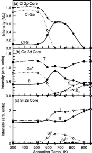
at 325 K and high-temperature annealing. All fitting was least-squares fitting.6,17,19Each component that consists of a pair of spin-orbit-split doublets is assumed to have the same Voigt line shape. Figure 3 plots the intensities associated with the relevant components. Before annealing at higher temperatures, the Cl 2 p core level关bottom spectrum in Fig. 2共a兲兴 has two components that correspond to emissions from the Cl atoms attached to Si and Ge 共labeled Si, and Cl-Ge兲, respectively.18 The difference between the binding en-ergy of Cl-Si and that of Cl-Ge, 0.64 eV, is rather large when the similar electronic structure of Si and Ge is considered.19 Without performing detailed corrections for defect effects, the chlorine coverage is nominally 1 ML because each sur-face atom共Si or Ge兲 has a dangling bond. The intensity ratio
共38:62兲 of the Cl-Ge and Cl-Si components indicates that the
Ge and Si coverage on the topmost surface layer is 0.38 and 0.62 ML, respectively, after 1 cycle of Ge ALE. The corre-sponding Si 2 p spectrum关the second from the bottom in Fig. 2共c兲兴 displays two spin-orbit doublets 共labeled Si⫹ and B兲. The chemical shift of Si⫹relative to B, which is⬇0.91 eV, is consistent with a nominal charge state of ⫹1 for Si di-rectly bonded to Cl.12,19 Consequently, the Si⫹ component originates from Si directly bonded to Cl, while the B com-ponent originates from bulk Si. Similarly, the corresponding Ge 3d line shape in Fig. 2共b兲 includes a dominated Ge⫹ component and another discernible B component. Ge atoms
adsorbed on the dimer layer contribute to the Ge⫹ compo-nent after Cl termination and will, therefore, account for the coverage of the Cl-Ge component共0.38 ML兲. The intensity of the B component is about one-ninth that of Ge⫹. Accord-ingly, the amount of Ge atoms that are present under the surface layer during the growth is ⬃0.04 ML if we neglect the effect of layer attenuation. Figure 3 shows that the an-nealing of the chlorine-terminated 0.4-ML-Ge/Si共100兲 sur-face substantially changes the relative intensity of many of the components, i.e., the population of the corresponding at-oms in the different thin-film layers. Below 810 K, the total intensity of the Cl 2 p spectra关curve T in Fig. 3共a兲兴 remains fairly constant, implying that most of the surface chlorine atoms remain on the surface. However, between 590 K and 740 K, the intensity of the Cl-Si component increases at the expense of the Cl-Ge component. When the surface is an-nealed at more than 740 K, the intensity of the Cl-Ge com-ponent vanishes; the corresponding Cl 2 p spectrum in Fig. 2共a兲 therefore includes only the Cl-Si component, suggesting that all the surface chlorine atoms are bonded only with Si atoms. The replacement of the surface Cl-Ge bonds with Cl-Si bonds is also evident from the change in intensity of the Ge 3d and Si 2 p spectra as shown in Figs. 3共b兲 and 3共c兲. Between 600 K and 740 K the intensity of the Si⫹ compo-nent increases, while the Ge⫹component gradually vanishes.
FIG. 2. Photoemission spectra 共circles兲 and fits 共solid curves兲 for the 共a兲 Cl 2p, 共b兲 Ge 3d, and 共c兲 Si 2p core levels of the 0.4-ML-Ge/Si共100兲 sample 关bottom spectra in 共b兲 and 共c兲兴, the same sample after Cl termination at 325 K and successive annealing for 60 s at various temperatures, as indicated. The 0.4-ML-Ge/Si共100兲 sample was obtained by growing Ge on a clean Si共100兲 surface with 1 cycle of Ge atomic layer epitaxy. The curves, labeled ClSi, ClGe, Ge⫹, B, Su, Sd, Si⫹, and Si2⫹, are a result of decomposition into
individual components, each with a pair of spin-orbit-split peaks. The B component is derived from the bulk, while S, Su, and Sdare
associated with the top surface layer. The Cl-Si, Cl-Ge, Si⫹, and Ge⫹ components are emitted from the Cl-Si-Si-Cl, Cl-Ge-Ge-Cl, and Cl-Si-Ge-Cl surface species. The B components correspond to Si and Ge in the subsurface region. The relative binding energy of the Si 2 p core levels refers to the Si 2 p3/2line of the B component
in the bottom spectrum. The relative binding energy of Cl 2 p and Ge 3d refers to the corresponding Si 2 p3/2line of the B component,
to eliminate the band-bending effect.
FIG. 3. Evolution of the intensity of the relevant photoemission spectra in Fig. 2. The Cl coverage is scaled to 1.0 ML, the Ge⫹ 共ClGe兲 coverage is 0.38 ML, and the Si⫹(ClSi) coverage is 0.62
After annealing at 740 K, the Ge 3d spectrum consists mainly of the B component and two smaller doublets, Suand Sd. In buckled Ge-Ge or Ge-Si dimers Su and Sd are com-monly attributed to emissions from the up and down atoms, respectively.20 Ge-Ge and Ge-Si dimers are evident in Fig. 1共b兲 as bright protrusions. Their paired dangling bonds typi-cally allow for a more efficient electron transfer between the tip and the surface, leading to the larger apparent height shown in the STM images.21The Si 2 p spectra in Fig. 2共c兲 show that the intensity of Si⫹increases during 810 K anneal-ing and that a new component 共labeled Si2⫹) emerges. The chemical shift of Si2⫹ relative to B, of around 1.82 eV, is consistent with a nominal charge state of ⫹2 for Si directly bonded to two Cl atoms. A theoretical study has found that after 1-ML Si is deposited on a Ge共100兲 surface, the surface energy of the Si-terminated structure is 0.38 eV/dimer higher than that of the segregated structure, in which Si indiffuses and occupies the second layer while Ge forms the surface layer.22The same study has also determined that the chlorine passivation of the Si/Ge共100兲 surface will dramatically re-verse the situation: the Cl-Si-Si-Cl monochloride surface is energetically favored over the Cl-Ge-Ge-Cl surface共with Si in the second layer兲, by 0.3 eV per dimer. Experimental work has verified that the thermodynamic driving force behind the energy differences is sufficiently large to cause the exchange of Cl-Ge bonds with Cl-Si bonds upon thermal activation.23 Interestingly, the same theoretical approach has found that a 1-ML-Ge film on a Si共100兲 surface remains thermodynami-cally stable after chlorine termination, since the Cl-Ge-Ge-Ge-terminated surface is 0.23 eV/dimer less than the segre-gated 共Cl-Si-Si-Cl-terminated兲 structure.24 The Cl-induced instability 共i.e., Si segregation兲 of ultrathin Ge films on a Si共100兲 surface found herein suggests that the hetero-Ge-Si bonds formed by the incorporation of Ge into the bulk Si environment will raise less chemical and strain energy than that determined by the aforementioned calculation. Rather, the energy difference between the Cl-Ge and Cl-Si bonds is
likely to be the dominant factor driving reactions in the Cl-terminated Ge films, as in the case of Cl:Si/Ge共100兲.23
C. Photoemission results for the 2-ML-GeÕSi„100…surface
Since ⬃0.4 ML Ge is deposited on the Si共100兲 surface during each Ge ALE cycle, the Ge coverage is estimated to be about 2.0 ML after 5 cycles of growth. The Cl 2 p, Ge 3d, and Si 2 p core-level photoemission spectra for the 2-ML-Ge/Si共100兲 sample were also measured and fitted, and the results are shown in Figs. 4 and 5. In Fig. 5, the intensity of the Cl-Ge, Cl-Si, Ge⫹, Si⫹, and B components reveals that the dimer layer of the 2-ML-Ge/Si共100兲 surface consists of 0.9 ML of Ge and 0.1 ML Si. After the sample is exposed to Cl2and annealed at 655 K, the coverage of the surface Cl-Si
bonds increases to 0.64 ML共from 0.1 ML兲 while Cl-Ge falls to 0 共from 0.9 ML兲. These observations imply that the re-maining 0.64-ML chlorine atoms only form Si-Cl bonds, so the rest of the surface mostly consists of Ge-Ge dimers. Un-like the 0.4-ML-Ge coverage, the Cl 2 p signal drops by about 40% and the Si2⫹ component is negligible. Although the reaction temperature (⬃655 K) is high enough to desorb GeCl2 on a Cl-terminated Ge共100兲 surface, chlorine is likely
to be desorbed in the form of Cl2 at this stage, since this
temperature is too low for SiCl2 desorption, and the amount
FIG. 4. Photoemission spectra 共circles兲 and fits 共solid curves兲 for the共a兲 Cl 2p, 共b兲 Ge 3d, and 共c兲 Si 2p core levels, similar to those in Fig. 2. The only difference is that the beginning sample is covered by a 2.0-ML-Ge layer after 5 cycles of Ge ALE are per-formed.
FIG. 5. Evolution of the intensity of the relevant photoemission spectra in Fig. 4. The Cl coverage is scaled to 1.0 ML; the Ge⫹ 共ClGe兲 coverage is 0.9 ML; and the Si⫹共CiSi兲 coverage is 0.1 ML.
of Ge atoms is not reduced 共as discussed in the following section兲. The reaction temperature (⬃655 K) is lower than
⬃750 K for the sample with a coverage of 0.4-ML Ge,
per-haps because partially recovered Ge-Ge dimers provide ad-ditional reaction pathways.
D. Selective Si etching
The etching product GeCl2 will be desorbed from the Ge共100兲 surface at ⬃620 K, much lower than ⬃900 K for SiCl2 to be desorbed from Si共100兲.10 In Fig. 2, we see that
the Cl 2 p signals decline above 810 K and vanish at 1000 K. The STM image 关Fig. 1共c兲兴, showing rows of buckled dimers, resembles the images taken before exposure to Cl2. The Ge 3d and Si 2 p spectra 关upper part of Figs. 2共b兲 and 2共c兲兴 after complete chlorine desorption can be seen to have line shapes that are very similar to those 关bottom of Figs. 2共b兲 and 2共c兲兴 before exposure to Cl2 at near RT.
Further-more, the integrated intensities of the Ge 3d spectra before and after the Cl2 adsorption and desorption are
approxi-mately equal. In the case of 2-ML coverage shown in Fig. 5共a兲 the integrated Cl 2p intensity has fallen significantly at
⬃600 K and fades away at ⬃850 K. However, the line
shape and the intensity of the Ge 3d and Si 2 p spectra after complete chlorine desorption关top parts of in Figs. 4共b兲 and 4共c兲兴 again resemble those before Cl2exposure关bottom parts
of spectra in Figs. 4共b兲 and 4共c兲兴. These findings suggest that the initial thin Ge layers共up to 2 ML兲 on the Si共100兲 surface will essentially be the same, before and after all the reactions occur, i.e., chlorine adsorption, Si segregation, exchange of Cl-Ge and Cl-Si, and chlorine desorption. Since the amount of Ge on the Ge/Si共100兲 surfaces remains the same, the ad-sorbed chlorine atoms will predominately leave the surface in the form of SiCl2共maybe some Cl2, but not GeCl2) during
annealing processes. In other words, Si will be preferentially consumed during the etching with Cl2molecules of ultra thin
Ge films on Si. Similar observations of selective etching
have also been reported for the Si/Ge system.23,25 These highly asymmetric Si and Ge etching rates on Ge/Si surfaces are unsurprising, given that there are no Cl-Ge bonds present on the surface above 740 K, even though the grown Ge lay-ers float on top on the relatively sharp Ge/Si interface.
IV. SUMMARY
This study utilizes core-level photoemission spectroscopy and scanning tunneling microscopy to examine the Cl-terminated ultrathin Ge films on Si共100兲 surfaces after an-nealing at various temperatures. The two techniques form a powerful surface probing combination. STM can yield a di-rect view of the atomic structure of the surface; photoemis-sion analysis of the Cl 2 p, Ge 3d, and Si 2 p core levels can provide a strong spectroscopic contrast between atoms in dif-ferent chemical environments. The STM images show that a dimerized structure remains the basic atomic building blocks throughout the chlorine termination and annealing processes of the thin Ge films on the Si共100兲 surface. An increase in the Cl-Si related core-level peaks, the vanishing of the core-level components due to the Cl-Ge species, and the loss of the STM contrast between the Cl-Si and Cl-Ge features clearly demonstrate that Si in the subsurface layers will be segre-gated to the surface to form Cl-Si bonds that will replace the Cl-Ge bonds at around 700 K. Above ⬃810 K, chlorine is desorbed in the form of SiCl2, although the top layer of the initial 2-ML-Ge/Si共100兲 surface is composed primarily of Ge-Ge dimers.
ACKNOWLEDGMENTS
The authors would like to thank the National Science Council of Taiwan for financially supporting this research under Contract No. NSC-90-2112-M-009-035. The Synchro-tron Radiation Research Center was also supported by the National Science Council, Taiwan.
*Electronic address: [email protected]
1See, for example, D.J. Paul, Adv. Mater.共Weinheim, Ger.兲 11, 191 共1999兲, and references therein.
2
K.N. Tu, J. Mayer, and L. Feldman, Electronic Thin Film Science for Electrical Engineers and Materials Scientists 共Macmillan, New York, 1992兲.
3C. Teichert, Phys. Rep. 365, 335共2002兲, and references therein. 4F. Liu, F. Wu, and M.G. Lagally, Chem. Rev.共Washington, D.C.兲
97, 1045共1997兲, and references therein.
5R. Larciprete, P. DePadova, C. Quaresima, C. Ottaviani, M. Peloi, and P. Perfetti, Phys. Rev. B 61, 16 006共2000兲.
6L. Patthey, E.L. Bullock, T. Abukawa, S. Kono, and L.S.O. Jo-hansson, Phys. Rev. Lett. 75, 2538共1995兲.
7D.-S. Lin, S.-Y. Pan, and M.-W. Wu, Phys. Rev. B 64, 233302 共2001兲.
8C.M. Aldao and J.H. Weaver, Prog. Surf. Sci. 68, 189共2001兲. 9J.J. Boland and J.H. Weaver, Phys. Today 51共8兲, 34 共1998兲. 10For review, see H.N. Waltenburg and J.T. Yates, Jr., Chem. Rev.
共Washington, D.C.兲 95, 1589 共1995兲.
11T.W. Pi, S.F. Tsai, C.P. Ouyang, J.F. Wen, and R.T. Wu, Surf. Sci.
488, 387共2001兲.
12T.D. Durbin, D.A. Lapiano-Smith, F.R. McFeely, F.J. Himpsel, and J.A. Yarmoff, Surf. Sci. 330, 147共1995兲.
13
W. Yang, Z. Dohnalek, W.J. Choyke, and J.T. Yates, Jr., Surf. Sci.
392, 8共1997兲.
14A. Szabo, P.D. Farrall, and T. Engel, Surf. Sci. 312, 284共1994兲. 15I. Lyubinetsky, Z. Dohnalek, W.J. Choyke, and J.T. Yates, Jr.,
Phys. Rev. B 58, 7950共1998兲.
16S.M. Cohen, T.I. Hukka, Y.L. Yang, and Mark P. D’Evlyn, Thin Solid Films 225, 155共1993兲.
17K.-H. Huang, T.-S. Ku, and D.-S. Lin, Phys. Rev. B 56, 4878 共1997兲.
18D.-S. Lin, J.L. Wu, S.-Y. Pan, and T.-C. Chiang, Phys. Rev. Lett.
90, 046102共2003兲.
19F.J. Himpsel, F.R. McFeely, J.F. Morar, A. Taleb-Ibrahimi, and J.A. Yarmoff, in Photoemission and Adsorption Spectroscopy of Solids and Interfaces with Synchrotron Radiation, Proceedings of the International School of Physics ‘‘Enrico Fermi,’’ Course CVIII, edited by G. Scoles共North-Holland, New York, 1991兲. 20R.I.G. Uhrberg, E. Landemark, and Y.-C. Chao, J. Electron
21D.-S. Lin, T.-S. Ku, and R.-P. Chen, Phys. Rev. B 61, 2799 共2000兲.
22M. C¸ akmak, S.C.A. Gay, and G.P. Srivastava, Surf. Sci. 454-456, 166共2000兲.
23M.W. Wu, S.-Y. Pan, W.H. Hung, and D.-S. Lin, Surf. Sci.
507-510, 295共2002兲.
24M.M. Bu¨lbu¨l, M. C¸ akmak, G.P. Srivastava, and K. Colakoglu, Surf. Sci. 507-510, 40共2002兲.
25
H. Takeuchi, T. Matsuua, and J. Murota, Appl. Phys. Lett. 77, 1828共2000兲.