國
立
交
通
大
學
電子工程學系 電子研究所碩士班
碩
士
論
文
切換感值之射頻電壓控制振盪器研究
The study of switched inductance radio frequency
voltage control oscillators with switched inductance
研 究 生:楊岱原
指導教授:荊鳳德 教授
切換感值之射頻電壓控制振盪器研究
學生 : 楊岱原 指導教授 : 荊鳳德 教授
國立交通大學
電子工程學系 電子研究所碩士班
摘要(中) 本論文描述如何設計金氧半壓控震盪器。討論如何利用單顆電感切換感值來達到 dual band 的效果。LC 壓控震盪器使用 TSMC 0.18um CMOS 製程,並經由 Ansoft designer 作 EM 分析跟 ADS 做電路驗證The study of switched inductance radio
frequency voltage control oscillators with
switched inductance
Student: Tai-Yuen Yang Advisor: Prof. Albert Chin
Department of Electronics Engineering & Institute of Electronics
National Chiao-Tung University
Abstraction
Design of CMOS Voltage-Controlled Oscillator(VCO) will be investigate in this thesis. We will discuss how to use one inductor to increase tuning range and achieve dual band. The LC tank VCO is implemented using TSMC 0.18um process. This simulation results with ADS and Ansoft designer.
ACKNOWLEDGEMENTS
能夠完成此篇論文,首先要感謝我的指導教授荊鳳德教授這兩年以來給我的 指導與鼓勵,使我在射頻積體電路的領域中有所了解,更學習到許多做學問的態 度與方法,在此向老師獻上最深最深的敬意。 感謝昶綜、張慈、維嘉學長跟瑄苓學姐在研究及學業上給我很多的幫助。還有一 起奮鬥的子倫、達道,大家一起做研究、打球、出遊,就像一個大家庭,使我在 兩年的碩士生活中留下許多美好的回憶。還要感謝溫老師及國家晶片中心在晶片 製作和量測上的大力幫忙,使我能夠順利的完成這篇論文。 最後還要感謝我的父母給我的栽培及鼓勵,以及在精神上給我許多的支 持,使我能順利走完碩士這段路程。其他要感謝的人還有很多,在此一併謝過 楊岱原 96年七月Contents
Abstract (in Chinese)...I
Abstract (in English)...II
Acknowledgements...III
Content...IV
Figure captions...VI
CHAPTER 1 INTRODUCTION...1
CHAPTER 2 OSCILLATOR THEORY...2
2.1 Oscillator fundamental...2
2.2 Thermal noise...5
2.3 MOSFET thermal noise...8
2.4 Flicker noise...10
2.5 Phase noise...12
2.6 Varactor ...16
2.6.1 Diode varactor...16
2.6.2 MOS varactor...18
2.7 Voltage control oscillator...21
2.8 Inductor...23
CHAPTER 3 LC TANK OSCILLATOR THEORY...26
3.1 LC tank oscillator architecture...26
3.2 LC cross coupled oscillator theory...29
3.3 Dual band LC VCO...31
3.3.1 Conventional Dual-band LC VCO...31
3.3.2 Switched Resonators...32
3.3.3 Switched Inductance...34
CHAPTER 4 SIMLATION AND MEASUREMENT...37
4.1 Simulation...37
CHAPTER 5 VCO DESIGN FLOW...42
5.1 Design procedure...42
5.2 Test procedure ...43
CHAPTER 6
CONCLUSION...44
References...45
Vita and Publication...47
FIGURE CAPTIONS
Figure 2.1 An oscillator may be modeled as the combination of an
amplifier and a feedback loop……….2
Figure 2.2 Addition of frequency-selective network……….3
Figure 2.3 One-port view of oscillator………4
Figure 2.4 Thermal noise model of a resistor……….5
Figure 2.5 Representation of resistor thermal noise by a current
source……….6
Figure 2.6 Noise generated in a low pass filter………...6
Figure 2.7 Thermal noise of a MOSFET…….………...8
Figure 2.8 Common gate output noise of a MOSFET………...9
Figure 2.9 Flicker noise corner frequency………10
Figure 2.10 Output spectrum of ideal and real oscillator……...……11
Figure 3.1 (a) Ideal, (b) realistic LC tank……….…15
Figure 3.2 (a) Tuned gain stage, (b) stage of (a) in feedback………..17
Figure 3.3 Output signal levels in a tuned stage………..…20
Figure 3.4 (a) Circuit to calculate the input impedance of cross
coupled pair, (b) equivalent circuit of cross coupled pair…………..22
Figure 4.1 Switch off (4 finger inductance) phase noise……….24
Figure 4.2 Switch off (4 finger inductance) tuning range…………...25
Figure 4.3 Switch on (2 finger inductance) phase noise………..26
Chapter1
Introduction
In the last few years, the research and development of direct conversion radio transceivers have dramatically increased due to the need for low-power, low-cost, and highly integrated transceiver chips. The radio-frequency(RF) front end of a wireless transceiver should have the ability to detect a wanted signal while very large interfering signals are present in adjacent channels. In particular,the characteristic of a local oscillator or a frequency synthesizer is very important in designing such systems. The CMOS process technology is very popular in the digital design for its low cost and systematic design methodology, but the traditional design of RF circuits is using single packaged Bipolar or GaAs process to accomplish its high performance and high operation frequency. This is due to the fact that the CMOS devices and circuit have many drawbacks such as low self-oscillation frequency, high performance and high operation frequency. In this thesis, we will discuss how to design VCO for dual band system.
Chapter2
Oscillator Theory
2.1 Oscllator fundamental
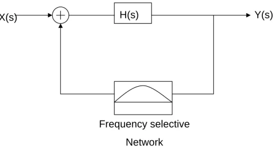
An oscillator circuit can be modeled as shown in Figure 2.1 as the combination of an amplifier with Gain A(jw) and a frequency dependent feedback loop H(jw)=βA. The general expression is
A A V V i o β β − = 1 (2.1)
Vi
A
Vo
β
Figure 2.1 An oscillator may be modeled as the combination of an
amplifier and a feedback loop
H(s)
Y(s)
Frequency selective
Network
X(s)
which states that the system will oscillate, provided βA = 1. At the frequency of oscillation, the total phase shift around the loop must be 360 degrees, and the magnitude of the open loop gain must be unity. The common emitter circuit provides 180 degree phase shift. If the circuit is used with feedback from collector to base, the feedback circuit must provide additional 180 degree phase shift. If a common base circuit is used, there is no phase shift between the emitter and collector signals, the feedback circuit must provide either 0 degree or full 360 degree phase shift. It is the function of the amplifier to generate the negative resistance or maintain oscillation by supplying an amount of energy equal to that dissipated. The selection of the circuit topology is dictated by several factors:
(a) Frequency of oscillation (b) Frequency tuning range (c) Choice of transistor (d) Type of resonator
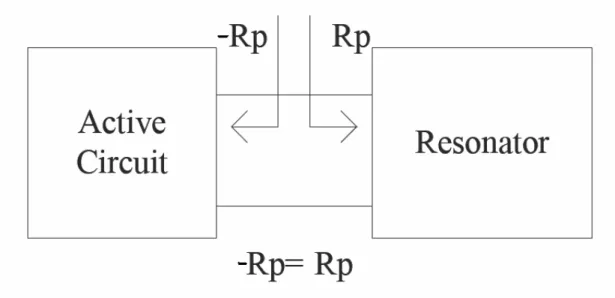
The above view of oscillators is called two-port model in microwave theory because the feedback loop is closed around a two-port network. By contrast the one-port model treats the oscillator as two one-port networks connected to each other as shown in Figure 2.3. The tank by itself does not oscillate indefinitely because some of the stored energy is dissipated in p R in every cycle. The idea in the one-port model is that an active network
generates an impedance equal to −Rp so that the equivalent parallel resistance seen by the
intrinsic, lossless resonator is infinite. In essence, the energy lost in p R is replenished by
Figure 2.3 One-port view of oscillator
A voltage controlled oscillator (VCO) is an oscillator where the principal variable or tuning element is a varactor diode. The VCO is tuned across its band by a "clear" dc voltage applied to the diode to vary the net capacitance applied to the tuned circuit. VCO's are used in virtually all spread Spectrum, RF and wireless systems. Every synthesizer and PLL has at least one VCO in it — thus designers should know something about them. Pick one of the links below to find out more information about this important subject.
2.2 Thermal noise
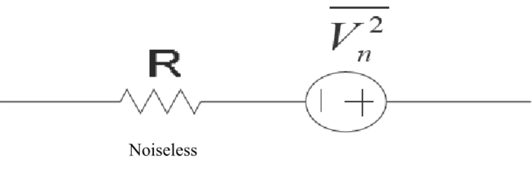
Resistor thermal noise
The random motion of electrons in a conductor introduces fluctuations in the voltage measured across the conductor even if the average current is zero. Thus, the spectrum of thermal noise is proportional to the absolute temperature.
Figure 2.4 Thermal noise model of a resistor
Noiseless
As shown in Figure 2.4, the thermal noise of a resistor R can be modeled by a series voltage source, with the one-sided spectral density
Where Κis the Boltzmann constant. Thus, we write where the overlie
indicates an average. to emphasize that 4KTR is the noise power per unit
bandwidth. To simplify the notation, we assume △f =1Hz, unless otherwise stated. The thermal noise of a resistor can be represented by a parallel current source as well. For the representations of Figure 2.4 and Figure 2.5 to be equivalent, we have , that is
Noiseless Resistor
R
Figure 2.5 Representation of resistor thermal noise by a current source
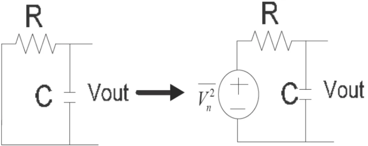
Consider a resistor R in parallel with a capacitor C. As a result of the random thermal agitation of the electrons in the resistor, the capacitor will be charged and discharged at random. The average energy stored in the capacitor will be:
Figure 2.6 Noise generated in a low pass filter
Where V 2 is the mean-square value of the voltage fluctuation impressed across the
capacitor. This equation can be proved by the theorem as follows:
Solving for the spectral density Sv(0) we get
Equation (2.5) is called Nyquist's Theorem and the symbol Sv(0) for the spectral density means that there is no frequency dependence. Noise with such a spectrum is called white.
2.3 MOSFETS thermal noise
This approach becomes more attractive with the observation that the mobility of charge carries in MOS devices increases at low temperature. MOS transistors also exhibit thermal noise. The most significant source is the noise generated in the channel. It can be proved that for long channel MOS devices operating in saturation, the channel noise can be modeled by a current source connected between the source and drain terminals (Figure 2.7) with a spectral density.
The actual equation reads, where gds is the drain-source conductance with
V
ds =0. The coefficient γ is derived to be equal to 2/3 for long channel transistors and mayneed to be replaced by a large value for submicron MOSFETs. It also varies to some extent with the drain-source voltage. The theoretical determination of γ is still under active research.
The maximum output noise occurs if the transistor sees only its own output impedance as the load. The output noise voltage is then given by
So the noise current of a MOS transistor decreases if the transconductance drop. For example, if the transistor operates as a constant current source, it is desirable to minimize its transconductance. SO, the Figure 2.8 may be a common source or a common gate stage, exhibiting the same output noise.
2.4 Flicker noise
The interface between the gate oxide and the silicon substrate in a MOSFET entails an interesting phenomenon. Since the silicon crystal reaches an end at this interface, many “dangling" bonds appear, giving rise to extra energy states. As charge carriers move at the interface, some are randomly trapped and later released by such energy states, introducing “Flicker" noise in the drain current. In addition to trapping, several other mechanisms are believed to general flicker noise. The flicker noise is more easily modeled as a voltage source in series with the gate and roughly given by
Where K is a process-dependent constant on the order of. In Figure 2.9 the noise spectral density is inversely proportional to the frequency. For this reason, flicker noise is also called 1/f noise. Note that Equation (2.9) does not depend on the bias current or the temperature. The inverse dependence of Equation (2.9) on WL suggests that to decrease 1/f noise, the device area must be increased. It is therefore not surprising to see devices having areas of several thousand square microns in low-noise applications. It is also believed that PMOS devices exhibit less 1/f noise than NMOS transistors because the former carry the holes in a “buried channel", at some distance form the oxide-silicon interface. Nonetheless, this difference between PMOS and NMOS transistors is not consistently observed.
We plot both spectral densities on the same axes (Figure 2.9). Called the 1/f noise “corne frequency", the intersection point serves as a measure of what part of the band is mostly corrupted by flicker noise.
This result implies that c f generally depends on device dimensions and bias current.
Nonetheless, since for a given L, the dependence is relatively weak, the 1/f noise corner is relatively constant, falling in the vicinity of 500KHz to 1MHz for submicron transistors.
2.5 Phase noise
As other analog circuits, oscillators are susceptible to noise. Noise injected into an oscillator by its constituent devices or by external may influence both the frequency and the amplitude of the output signal. In most cases, the disturbance in amplitude is negligible or unimportant, and only the random deviation of the frequency is considered. The latter can be viewed as random variation in the period or deviation of zero crossing points from their ideal position along time axis. For a nominally periodic sinusoidal signal we can write , where is small random excess phase representing variations in period. The function ( ) n f t is called phase noise. Note that for < 1 rad, we have
; that is, the spectrum of is translated to .
In RF applications, phase noise is usually characterized in the frequency domain. For an ideal sinusoidal oscillator operating at , the spectrum assumes the shape of an impulse, whereas an actual oscillator, the spectrum exhibits skirts around the carrier frequency (Figure 2.10). To quantify phase noise, we consider a unit bandwidth at an offset Δw with respect to , calculate the noise power in this bandwidth, and divide the result by the
carrier (average) power.
It is conventionally given the units of decibels below the carrier per Hertz (dBc/Hz) and is define as shown in Equation (2.12) where represents the single sideband power at a frequency offset, Δw , from the carrier in a measurement bandwidth of 1Hz as shown in Figure 2.10, and is the total power under the power spectrum. The advantage of in Equation (2.12) is its ease of measurement. Its disadvantage is that is shows the sum of both amplitude and phase variations; it does not show them separately in a circuit. It is often important to known the amplitude and phase noise separately because they behave differently in a circuit. For instance, the effect of amplitude noise can be reduced by amplitude limiting, while the phase noise cannot be reduced in an analog manner. Therefore, in most practical oscillators, is dominated by its
phase portion, , known as phase noise, which will be simply denoted as
, unless specified otherwise. For example, if the carrier power is –2 dBm and the noise power measured in a 1kHz bandwidth at an offset of 1 MHz is equal to –70 dBm then the phase noise is specified as –70dBm+2dBm-30dB=-98dBc/Hz, where dBc means “ in db with respect to carrier" [1].
Phase noise is measured in the frequency domain, and is expressed as a ratio of signal power to noise power measured in a 1 Hz bandwidth at a given offset from the desired signal. A plot of responses at various offsets from the desired signal is usually comprised of three distinct slopes corresponding to three primary noise generating mechanisms in the oscillator, as shown in Figure 2.11. Noise relatively close to the carrier (Region A) is called Flicker FM noise; its magnitude is determined primarily by the quality of the crystal. Noise in Region B of Figure 2.11, called "1/f" noise, is caused by semiconductor activity. Design techniques employed in low noise crystal oscillators limit this to a very low, often insignificant value. Region C of Figure 2.11 is called white noise or broadband noise.
It is important to determine from measurements, diminishing the predictive power of the phase-noise equation. Furthermore, the model asserts that , the boundary between
the and regions, is precisely equal to the 1/f corner of device noise. However, measurements frequently show no such equality, and thus one must generally treat as an empirical fitting parameter as well. Also, it is not clear what the corner frequency will be in the presence of more than one noise source with 1/f noise contribution. Last, the frequency at which the noise flattens out is not always equal to half the resonator bandwidth, . The ideal oscillator model suggest that increasing resonator Q and signal amplitude are ways to reduce phase noise. Referring to the ideal case depicted in Figure 2.12(a), we note that the signal of interest is convolved with an impulse and thus translated to a lower (and a higher) frequency with no change in its shape. In reality, however, the wanted signals may be accompanied by a large interferer in adjacent channel,
and the local oscillator exhibits finite phase noise [Figure 2.12(b)]. When the two signals are mixed with the LO output, the down converted band consists of two overlapping spectra, with the wanted signal suffering from significant noise due to the tail of the interferer. This effect is called “reciprocal mixing". Shown in Figure 2.12(c), the effect of phase noise on transmit path is slightly different. Suppose a noiseless receiver is to detect a weak
2.6 Varactors
2.6.1 Diode varactor
The varactor diode symbol is shown below with a diagram representation.
When a reverse voltage is applied to a PN junction, the holes in the p-region are attracted to the anode terminal and electrons in the n-region are attracted to the cathode terminal creating a region where there is a little current. This region, the depletion region, is essentially devoid of carriers and behaves as the dielectric of a capacitor. The depletion region increases as reverse voltage across it increases; and since capacitance varies inversely as dielectric thickness, the junction capacitance will decrease as the voltage across the PN junction increases. So by varying the reverse voltage across a PN junction the junction capacitance can be varied. This is shown in the typical varactor
voltage-capacitance curve below. The capacitance is then a function of the width of the depletion region, which is controlled by the reverse voltage (VR). If a small VR is applied across the junction, the width is correspondingly small, and hence a large capacitance results. If VR is increased, the junction width also increases, and a smaller capacitance is obtained. Hence, by changing the reverse voltage, the junction capacitance is also changed, and the wanted functionality is obtained.
Major varactor considerations are:
(a) Capacitance value (b) Voltage
(c) Variation in capacitance with voltage (d) Maximum working voltage
2.6.2 MOS varactor
A MOS transistor with drain, source, and bulk (D, S, B) connected together realizes a MOS capacitor with capacitance value dependent on the voltage Vgs between B and gate (G). The cross sectional view of the NMOS varactor is shown in Figure 2.14. In the case of an NMOS capacitor, an inversion channel with mobile holes builds up for , where is the threshold voltage of the transistor. The condition guarantees that the MOS capacitor works in the strong inversion region, the region where the MOS device shows a transistors behavior. On the other hand, for some voltage , the MOS device enters the accumulation region, where the voltage at the interface between gate oxide and semiconductor is positive and high enough to allow electrons to move freely. Thus, in both strong inversion and accumulation region the value of the MOS
capacitance Cgs is equal to , where S and tox are the transistor channel area and the oxide thickness, respectively [3].
A very attractive realization of an MOS varactor is given by the pMOS device working in the depletion and accumulation regions only. This solution allows for the implementation of a MOS varactor with a large tuning range (Cmos does not climb back to Cox, since
accumulation-mode MOS capacitor, we must make sure that the formation of the strong, moderate, and weak inversion regions is inhibited, which requires the suppression of any injection of holes in the MOS channel. This, in turn, can be accomplished with the removal of the D/S diffusions (p+-doped) from the MOS device. At the same time, we can implement the bulk contacts (n+) in the place left by D/S, as shown in Figure 2-15, which minimizes the parasitic N-well resistance of the device [4].
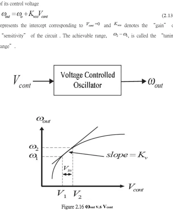
2.7 Voltage control oscillator
An ideal voltage control oscillator is a circuit whose output frequency is a linear function of its control voltage
represents the intercept corresponding to and denotes the “gain" or “sensitivity" of the circuit . The achievable range, , is called the “tuning range".
Figure 2.16
ω
out v.s VcontCenter frequency : The center frequency is determined by the environment in which
the VCO is used. Today CMOS VCO's achieve center frequencies as high as 1.8GHz, 2.4GHz and 5.2~5.8GHz.
The center frequency of some CMOS oscillators may vary by a factor of the two at the extremes of process and temperature, thus mandating a sufficiently wide (≧ 2×) tuning range to guarantee that the VCO output frequency can be driven to the desired value. An important concern in the design of VCO's is the variation of the output phase and frequency as a result of noise on the control line. For a given noise amplitude, the noise in the output frequency is proportional to because Thus, to minimize the effect of noise in , the VCO gain must be minimized, a constraint in direct conflict with the require tuning range. In fact, if, as shown in Figure 2.16, the allowable range of is from V1 to V2 and the tuning range must span at least
ω
1 toω
2, thenmust satisfy the following requirement:
Output amplitude : It is desired to achieve large output oscillation amplitude, thus
making the waveform less sensitive to noise. The amplitude trades with power dissipation, supply voltage, and tuning range. Also, the amplitude may vary across the tuning range, an undesirable effect.
Power dissipation: In analog circuit, oscillators suffer from trade-offs between speed,
power dissipation, and noise.
Supply and common mode rejection : Oscillators are quite sensitive to noise,
especially if they are realized in single-ended form. The design of oscillators for high noise immunity is a difficult challenge. So that noise may be coupled to the control line of a VCO as well. For these reasons, it is preferable to employ differential paths for both the oscillation signal and the control line.
Output signal purity : Even with a constant control voltage, the output waveform of a
VCO is not perfectly periodic. The electronic noise of the devices in the oscillator and supply noise lead to noise in the output phase and frequency. These effects are quantified by “Jitter" and “Phase Noise" and determined by the requirements of each application [2].
2.8 Inductor
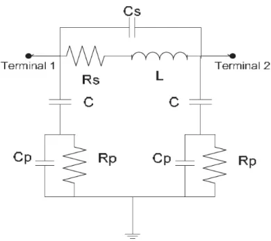
In integrated RF works in silicon, inductors are normally implemented as a planar spiral-shaped metal. Figure 2.17 shows the top view of an example spiral inductor in silicon, realized using the top metal layer while the metal layer below the top metal layer is used for an interconnection for terminal 2. Figure 2.18 shows an equivalent electrical circuit model for the spiral inductor, obtained using an electromagnetic simulation. In this model, L, Rs, Rp, and Cp represent inductance, metal loss due to the skin effect, substrate loss, and metal-substrate capacitance, respectively. Cs accounts for the metal overlap capacitance between the top metal and the metal below. Using Cadence, measures the quality factor, Q of the spiral inductor (See the note below) over the frequency range.
Figure 2.18 Spiral inductor equivalent electrical circuit model
is discussed in class, the quality factor, Q is originally defined for a “ resonator " as:
where is the resonance frequency. For a given resonator whose resonance frequency is fixed, Q is not a function of frequency. Since inductors are not resonators, the original Q definition above cannot be used for inductors. However, the following frequency -dependent Q definition may be used instead as the quality factor for inductors:
It can be easily shown that Q (ω) in (2.16) is on the same order as, but not exactly the same as,
where Z (ω) is the frequency-dependent input impedance of a given inductor. RF engineers traditionally choose to use (2.15) over (2.16) due to the simplicity of (2.17). In
the problem above, we can evaluate the Q of the spiral inductor using (2.17) while the input impedance Z (ω) shown in Figure 2.18 can be measured using Cadence.
CHAPTER 3
LC TANK OSCILLATOR THEORY
3.1 LC tank oscillator architecture
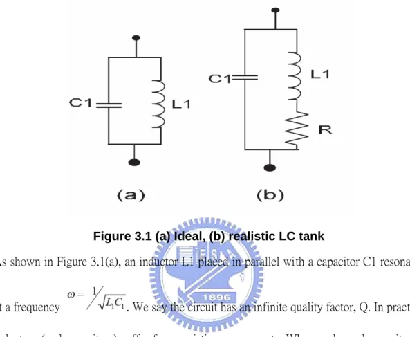
Figure 3.1 (a) Ideal, (b) realistic LC tank
As shown in Figure 3.1(a), an inductor L1 placed in parallel with a capacitor C1 resonates
at a frequency . We say the circuit has an infinite quality factor, Q. In practice, inductors (and capacitors) suffer from resistive components. When a charged capacitor is connected to an inductor, the conventional analysis is to equate the voltage across the capacitor with the voltage across the inductor.
(3.1)
Differentiating, we get
(3.2)
(3.3)
The traditional analysis assumes that when current is switched into the inductor, it appears instantaneously at all points in the inductor; the use of the single, lumped quantity L implies this. Similarly, it is assumed that the electric charge density at all points in the capacitor is the same; that there are no transient effects such that the charge density is greater in certain regions of the capacitor plates.
For this circuit reader can show that the equivalent impedance is given by
(3.4)
(3.5)
that is, the impendence does not go to infinite at any s=jω. We say the circuit has a finite
Q. The magnitude of Zeq in (3.5) reaches a peak in the vicinity of , but the actual resonance frequency has some dependency on Rs.
Let us now consider the “tuned" stage of Figure 3.2(a), where an LC tank operatesas
the load. At resonance, and the voltage gain equal (Note that the gain of the circuit is very small at frequencies near zero). Also from Figure 3.2(b), the frequency dependent phase shift of the tank never reaches .Thus, the circuit does not oscillate.
Figure 3.3 Output signal levels in a tuned stage
Before modifying the circuit for oscillatory behavior, let us observe another interesting property of the gain stage of Figure 3.2 (a) that distinguishes it from a common-source topology using a resistive load. Suppose, as shown in Figure 4.3, the stage is biased at a drain current. If the series resistance of Lp is small, the dc level of Vout is close to Vdd. We expect Vout to be an inverted sinusoid with an average value near Vdd because the inductor cannot sustain a large dc drop. In other average value of Vout deviates significantly fromVdd, then the inductor series resistance must carry an average current greater than I1. Thus, the peak output level in fact exceeds the supply voltage, an import and often useful attribute of the LC load. For example, with proper design, the output peak-to-peak swing can be large than Vdd.
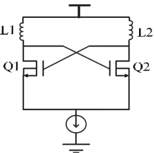
3.2 LC cross coupled oscillator theory
Calculating the impedance seen at the collector of Q1 and Q2 as shown in Figure 3.4(a),
we note that positive feedback yields (shown in Figure 3.4 (b) and Equations 3.6-3.10). Thus, if |Rin| is larger than or equal to the equivalent parallel resistance of the tank, the circuit oscillates. This topology is called a negative-Gm oscillator.
Figure 3.4 (a) Circuit to calculate the input impedance of cross coupled pair, (b) equivalent circuit of cross coupled pair
(3.6) (3.7) (3.8)
(3.9)
3.3 Dual-band LC VCO
3.3.1 Conventional Dual-band LC VCO
Basically the circuit is derived using two similar half circuits as that shown in Figure 3.6 The circuit is formed by a pair of nMOS (MN1 and MN2) transistors and pMOS (MP1 and MP2) transistors which are cross coupled to create positive feedback loops in parallel with LC (L1, L2, L3 and L4) resonators. The capacitors C are implemented by the diode varactors JV1, JV2, JV3 and JV4 to control the resonant frequency of the LC tanks. The two half circuits share the same dc current, so that they have two frequency outputs and only one dc power dissipation, leading to saving the power. The Cp is used to decouple the ac signals from the upper and lower half circuits. The circuit uses single VDD and GND that produce dual-band frequencies at the same time. However, the design of dual-band VCO's presents a considerable challenge because of the simultaneous requirements for wide frequency range, lower current consumption and low power consumption.
3.3.2 Switched Resonators
A possible way to achieve a wide tuning range is to use a switched capacitor bank in a resonator. To qualitatively discuss the need for a switched resonator over a switched capacitor bank, consider the – VCO shown in Fig.3.7
Figure 3.7
Schematic of a dual-band VCO.
Fig. 3.8(a) and (b) shows switched resonators including mutual inductance (M). The inductance seen between ports 1 and 2 are changed by turning the switch transistor on and off. The equivalent circuit of the switched resonator is shown in Fig. 3.8(c). In the case that port 2 is grounded and that and have no mutual effect (M=0), the resonator is simplified into the circuit in Fig. 2(d) when the switch is on, and into the circuit in Fig. 2(e) when off. When the switch is off, the inductance of switched resonator is largely determined by the two inductors while the capacitance is determinedbythe parasitic capacitances ( and ) of the inductors and the capacitances ( and ) at the drainoftheswitchtransistor.Theextractedinductanceusingmeasurements and the simple inductor model is lower due to the effects of in series with , and of the switch transistor (M4 ). When the switch is on, the channel resistance is close to zero.Theinductance and capacitance of the switched resonator are switched by shorting out L2, the capacitances associated with L2,L1,and the switch transistor.The
inductance is approximately L1 and the capacitance is Cp1, thus, leading to simultaneous decreasesof inductance and capacitance.
3.3.3 Switched Inductance
Switched resonators circuit compare to conventional dual band VCO circuit, less power consumption and smaller die area. But switched resonators circuit still needs two inductor, so I have a new idea to use an inductor achieving two inductance.(Figure3.9)
Switch
Metal6(2finger)
Metal5(4finger)
Figure 3.9
Switched Inductance diagram
When switch off, the inductance seems to Tsmc 0.18um four fingers spiral inductor. When switch on, the inductance seems to Tsmc 0.18um two fingers spiral inductor. But when switch on (two fingers), we must think about the MOS parasitic resistance the mutual inductance between inner circle and outer circle. So my method is using RF model from Tsmc to import Ansoft Designer and run EM analysis. But we still consider MOS switch parasitic capacity and resistance. RF MOS model is as Figure3.10.
Rg Source C1 Rs C2 C3 Gate Drain Rd
Figure 3.10
RF MOS Model
So MOS main parasitic capacity is approach (C1//C3)+C2.And MOS main parasitic resistance is approach Rd+Rs
C1=0.181*N*L*1e6+0.153*N+0.331
C2=0.0713+0.0842*N*W*1e6/(L*1e6+0.9)+1.051*N*(L*1e6+0.54)/(W*1e6+9.8) C3=1.649*N*(L*1e6+0.54)/(0.1*W*1e6+4)+0.158*W*1e6+0.737
Rd=0.005417*(L*1e6+0.54)*(Nd+2/Nd)+0.0929*(W*1e6+2.94)/Nd+1.625/(1.43+(N
d-1)*(L*1e6+0.54)) Where Nd=int((N+1)/2)
Rs=(0.0325*(L*1e6+0.54)*(2*Ns+1/Ns-3)+8.666/Ns+0.4485)/(W*1e6)
Where Ns=int(N/2+1)
If we decide MOS size, then we can estimate C1,C2,C3,Rd,Rs value approximately. So we include these informations in our circuit design. My circuit is a conventional cross-couple type(Figue3.11) to generate negative resistance to cancel resistance because of LC tank unlimited Q value.
R1 C1 C2 R2 Vcontrol Ic
Figure 3.10
cross-couple circuit
First we want varactor C2 to have maximum variable capacitance. Because we must control C2 both sides voltage to make sure capacitance, then we add C1 so C2 both sides voltage doesn’t change with oscillator. If we want C2 to dominate capacitance, the C1 capacitance must be biggest as we can accept.R1, R2 also must be large enough so it seems AC open. We use a NMOS and give voltage from it’s gate to make a current source and control current. Output buffer exist for signal isolation between LC tank and measure instrument.
Signal in
Signal out
Figure 3.11
Output buffer
We adopted a fixed current source and common-drain architecture. A fixed current source can avoid that output buffer current changes with signal in. If the output buffer current changes with signal in, the signal out power can’t export stably.
CHAPTER 4
Simulation And Measurement
4.1 Simulation
m1 noisefreq= vo.pnfm=-121.3 dBc1.000MHz 0.2 0.4 0.6 0.8 0.0 1.0 -120 -100 -80 -60 -140 -40 noisefreq, MHz vo. pnf m , dBc m1Figure 4.1 Switch off (4 finger inductance) phase noise
0.2 0.4 0.6 0.8 1.0 1.2 1.4 1.6 1.8 0.0 2.0 2.25 2.30 2.35 2.40 2.20 2.45 HB.vc fre q [1 ], G Hz
Figure 4.2 Switch off (4 finger inductance) tuning range
m1 noisefreq= vo.pnfm=-115.7 dBc1.000MHz 0.2 0.4 0.6 0.8 0.0 1.0 -100 -80 -60 -120 -40 noisefreq, MHz vo .p nf m , dB c m1 Figure 4.3 Switch on (2 finger inductance) phase noise
0.2 0.4 0.6 0.8 1.0 1.2 1.4 1.6 1.8 0.0 2.0 5.0 5.2 5.4 5.6 5.8 4.8 6.0 HB.vc fr eq [1 ], G H z
Figure 4.4 Switch on (2 finger inductance) tuning range
freq. tuning range4.8GHz~6GHz output buffer swing=0.4V
4.2 Measurement
Figure 4.5 Switch off (4 finger inductance) phase noise
Figure 4.7 Switch on (2 finger inductance) phase noise
Figure 4.8 Switch on (2 finger inductance) tuning range
freq. tuning range4.2GHz~5.4GHz output buffer swing=0.38V
CHAPTER 5
VCO DESIGN FLOW
5.1 Design procedure
The simulation software Spectre RF is used to design analogy circuit. After the layout of the circuit is finished, the LPE (layout parameter extraction) is done to extract parasitic components which is put into the circuit and we simulated complete circuit again.
System Spec
Circuit Design
Schematic Simulation
Layout(DRC,LVS)
Layout Simulation
Finish
Yes
Yes
No
No
5.2 Test procedure
Measurement of output spectrum and output power performances were obtained using an Adventest R3162 spectrum analyzer.
Power Supply
Ammeter
Die under PCB broad Spectrum Analyzer
Figure 5.2 Experimental set-up
On-board measurements of output spectrum and output power performances were obtained using an Adventest R3162 spectrum analyzer.
CHAPTER 6
CONCLUSION
In first band (switched off,2.2~2.45G),simulation meets measurement mostly, but in measurement spectrum signal isn’t pure. Because my PCB board transmission line width is matching for 5GHz (26mil in 5GHz, S11=-28dB), so spectrum in 5GHz is much pure than 2GHz (26mil in 2GHz, S11=-13dB). Spectrum in 5GHz, we can see the appearance of tuning range shift. Because we ignore inductor’s outside metal of the inner circle when switch on. This also has inductance and generates mutual inductance with inner circle. So these reason made real inductance over exception. And switch’s parasitic also effects Q value of inductor, so phase noise in measurement is higher than simulation.
Compare with report before[20] Parameter Dual band
VCO(low)
Dual band VCO(high)
This Work(low) This
Work(high) Current 8.97mA(only Core) 8.8mA(only Core) 4mA(all circuit) 4.2mA(all circuit) Tuning Range 823MHz~867MHz (44MHz) 1640MHz~1814MHz (174MHz) 2.15GHz~2.4GHz (250MHz) 4.2GHz~5.4GHz (1.2GHz) Phase noise(1MHz) -125dBc/MHz -123dBc/MHz -118dBc/MHz -106.3dBc/MHz Die Size(mm^2) 1.3x0.69 1.3x0.69 1.38x0.77 1.38x0.77
Reference
[1] B. Razavi, RF microelectronics, Prentice Hall PTR, 1998.
[2] B. Razavi, Design of analog CMOS integrated circuits, McGraw-Hill, 2001.
[3] P. Andreani and S. Mattisson, “On the use of MOS varactors in RF VCO's," IEEE J. Solid State Circuits, Pages: 905–910, June 2000.
[4] P. Andreani and S. Mattisson, “A 1.8-GHZ CMOS VCO tunded by an accumulation mode MOS varactor," ISCAS 2000 Geneva, Pages: 315–318, 28-31 May 2000.
[5] T. C. Weigandt, B. Kim and P. R. Gray, “Analysis of timing jitter in CMOS ring oscillators," Proc. ISCAS, Pages: 27–30, 30 May-2 June 1994.
[6] A. A. Abidi and R. G. Meyer, “Noise in relaxation oscillators," IEEE J. Solid State Circuit, Pages: 794–802, Dec. 1983.
[7] C. H. Park and B. Kim, “A low-noise 900-MHz VCO in 0.6μm CMOS," IEEE J. Solid State Circuits, Pages: 586–591, May 1999.
[8] Y. A. Eken and J. P. Uyemura, “A 5.9-GHz voltage-controlled ring oscillator in 0.18μm CMOS," IEEE J. Solid State Circuits, Pages: 230–233, Jan 2004.
[9] P. Andreani and H. Sjoland, “Tail current noise suppression in RF CMOS VCO's," IEEE J. Solid State Circuits, Pages: 342–348, Mar. 2002.
[10] J. Maget, M. Tiebout and R. Kraus, “Influence of novel MOS varactors on the performance of a fully integrated UMTS VCO in standard 0.25μm CMOS technology," IEEE J. Solid State Circuits, Pages: 953–958, July 2002.
[11] Z. Shu, K. L. Lee and B. H. Leung, “A 2.4-GHz ring oscillator based CMOS frequency synthesizer with a fractional divider dual PLL architecture,” IEEE J. Solid State
Circuits, Pages: 452–462, Mar 2004.
[12] M. A. Do, R. Y. Zhao, K. S. Yeo and J. G. Ma, “New wide band/dual band CMOS LC voltage controlled oscillator Circuits,” IEE Proceedings, Devices and Systems, Pages:
[14] B. Razavi, “A 1.8GHz CMOS voltage–controlled oscillator,” (ISSCC) digest of
technical papers, San Francisco, USA, Pages: 388–389, Feb. 1997.
[15] H. Jacobsson, B. Hansson, H. Berg and S. Gevorgian, “Very low phase-noise fully-integrated coupled VCO's," Radio Frequency Integrated Circuits (RFIC) symposium, Pages: 467–470, 2-4 June 2002.
[16] C. Yul Cha and S. Lee, “A complementary Colpitts oscillator based on 0.35 μm CMOS technology," Solid State Circuits conference, Proceedings of the 29th
European, Pages: 691–694, 16-18 Sept. 2003.
[17] H. Jacobsson, B. Hansson, H. Berg and S. Gevorgian, “Very low phase noise fully integrated coupled VCO's," Radio Frequency Integrated Circuits (RFIC) symposium, Pages: 467–470, 2-4 June 2002.
[18] C. Y. Cha and S. G. Lee, “Overcome the phase noise optimization limit of differential LC oscillator with asymmetric capacitance tank structure," Radio Frequency
Integrated Circuits (RFIC) symposium, Pages: 583–586, 6-8 June 2004.
[19] F. Svelto and R. Castello, “A bond-wire inductor-MOS varactor VCO tunable from 1.8 to 2.4 GHz,” IEEE Trans. Microwave Theory and Tech., Pages: 403–407, Jan. 2002.
[20] P. Park, C.-S. Kim, M.-Y. Park, S.-D. Kim, and H.-K. Yu, “Variable inductance multilayer inductor with MOSFET switch control,” IEEE Electron Device Lett., vol. 25, no. 3, pp. 144–146, Mar. 2004.
Vita and Publication
姓 名: 楊岱原
出生日期: 中華民國七十年八月十四日
學經歷:
國立成功高級中學 (86 年9 月~89 年6 月)
國立交通大學電子工程學系 (89 年9 月~94 年6 月)
國立交通大學電子研究所碩士班 (94 年9 月~96 年7 月)
發表著作:
1. H. L. Kao, D. Y. Yang, Albert Chin, and S. P. McAlister, “2.4/5 GHz Dual-Band LC VCO using Variable Inductor and Switched Resonator,” IEEE MTT-S Int’l Microwave Symp. Dig., pp., June 12-17, 2007.