2D Self-Bundled CdS Nanorods with
Micrometer Dimension in the Absence of
an External Directing Process
Chia-Cheng Kang,†Chih-Wei Lai,†Hsin-Chieh Peng,†Jing-Jong Shyue,‡,* and Pi-Tai Chou†,* †
Department of Chemistry, National Taiwan University, Taipei 106, Taiwan, and‡
Research Center for Applied Science, Academia Sinica, Taipei 115, Taiwan
I
n addition to zero dimensionalsemi-conductor nanoparticles (also referred to as “quantum dots”), one-dimensional semiconductor nanocrystals that are sev-eral nanometers in diameter and have dif-ferent aspect ratios have also drawn much attention because of their fascinating size-dependent optical and electronic proper-ties. Pioneering works have unravelled unique linear polarized emission along the c-axis of crystals in CdSe and CdSe/CdS (core/shell) nanorods owing to their
intrin-sic dipolar structure.1–5Concurrently,
tre-mendous efforts have been devoted to the alternative synthesizing routes and the growth mechanism of semiconductor
nanocrystals.6–22Regarding the updated
progress, the Gibbs⫺Curie⫺Wulff theorem,
which concludes that minimization of total free energy in the reaction system is essen-tial to determine the crystalline shapes, may not be valid in explaining the anisotropic shape-controlling models of
nanocrystals.1,6–8,13,16Alternatively, the
models of effective-monomer,1,7,8,16
selective-adsorption,6and the presence of
“magic-sized” nuclei7,13turn out to be more
appropriate in rationalizing the kinetic
growth mechanism of the semiconducting nanorods.
Elongated semiconducting nanocrys-tals, such as CdSe or CdTe nanorods, are highly attractive for photovoltaic applica-tions due to their ability to transport
charges along the long axis.23,24
Nowa-days, state-of-the-art synthetic techniques can provide nanorods with uniform size and
shape distribution.6–8,11–13,19These
nano-rods can also offer a route to systematically study the effect of shape on the phase be-havior, namely the liquid crystalline phase and self-assembled superstructures. More-over, macroscopic assembly of nanorods might have advantages for applications in photovoltaic, field emission, and data stor-age devices. Onsstor-ager first claimed that anisotropic particles may form a liquid crys-talline phase, which shows long-range or-dering in orientation but disoror-dering in
po-sition.25Further research supports this
notable theory, and large-scale spatial orga-nization has been obtained by depositing concentrated solutions of CdSe and CdSe/ CdS heterostructure aggregates onto
substrates.26–28Recently, Alivisatos and
co-workers reported the assembly of CdS nan-orod superlattices by the combination of a DC electric field and controlled solvent
evaporation.29During gentle evaporation
of toluene, the CdS nanorods were confined into an array by the DC electric field, mak-ing the long axis of the rods in the same di-rection. The net effect was a 2D superlat-tice “standing” on the substrate.
Concurrently, Gupta et al. discovered
simi-lar results with CdSe nanorods.30The
sur-face of CdSe nanorods was modified by polyethylene oxide (PEO) or polystyrene (PS). Poly(methyl methacrylate) (PMMA) or poly(3-hexylthiophene) (P3HT) was added to the CdSe solution to serve as the poly-*Address correspondence to
chop@ntu.edu.tw, shyue@gate.sinica.edu.tw. Received for review January 11, 2008 and accepted March 25, 2008. Published online April 5, 2008. 10.1021/nn800020h CCC: $40.75
© 2008 American Chemical Society
ABSTRACTIn the absence of an external direction-controlling process, exclusive self-bundled arrays of CdS nanorods are formed using a facile solution-based method involving trioctylphosphine (TOP) and
tetradecylphosphonic acids (TDPA) as cosurfactants. CdS self-bundled arrays with an area of as large as 2.0m2 could be obtained. A detailed mechanistic investigation leads us to conclude that the matching in nanorod concentration, intrinsic properties of CdS, and the hydrocarbon chains of the surfactants between adjacent CdS rods play key roles in the assembly. In sharp contrast to the defect dominant emission in solutions, the self-bundled CdS nanorods exhibit optical emission nearly free from the defect-states, demonstrating their potential for applications in luminescence and photovoltaic devices.
KEYWORDS:CdS · nanorod · self-assembly · semiconductor · nanocrystal
ARTICLE
Downloaded by NATIONAL TAIWAN UNIV on July 27, 2009
mer matrix. In the presence of an electricfield, alkane-covered CdSe nanorods were corralled into densely
packed arrays because of the polymer⫺ligand
inter-action. Since poly(3-hexylthiophene) is a common photoactive polymer, the polymer-nanorod assem-bly appears to have the potential for photovoltaic applications. In 2007, Ryan’s group reported super-crystallization of CdS nanorods into perpendicular
superlattices.31Via the assistance of highly oriented
pyrolytic graphite (HOPG), hexagonal oriented do-mains of CdS nanorod bundles can be obtained on a variety of substrates without an external electric field. More recently, Manna’s group synthesized CdS nanorods through a seeded-growth approach in which CdSe nanoparticles were used as seeds to
pro-duce asymmetric core⫺shell CdSe/CdS nanorods.
By evaporating the solvent at the toluene/water in-terface or under the applied electric field, large areas of vertically aligned nanorods arrays were
ob-tained.32
To investigate the internal force that laterally bunches nanorods together, Korgel and co-workers
cal-culated the dipole⫺dipole attractive force and van der
Waals attraction of self-alignment CdS nanorods.33The
result of calculations suggested that side-by-side align-ment was more favorable than the end-to-end case. Conversely, experimental results from the same report
showed networks of end-to-end stripes instead of side-by-side assembly, and it was thus proposed that the for-mation of stripes was kinetically limited, or mediated, by solvent evaporation. Also, He et al. studied the
self-assembly of CdSe nanorods at the oil⫺toluene water
in-terface.34During the solvent evaporation, as the
sur-face area of the droplet decreases, the in-plane compression and the interfacial tension play important roles in the formation of two-dimensional assembled structures.
Although the bundling of 1D semiconductor nano-structures has been theoretically predicted and experi-mentally observed, exclusively well-aligned arrays of nanorods without an external direction-controlling force, for example, applying an external electric field or evaporation in the presence of ordered substrate, have not been reported yet. In this work, upon capping CdS with tri-n-octylphosphine (TOP) and tetradecyl-phosphonic acid (TDPA) with the optimum ratio, exclu-sive formation of arrays of self-bundled CdS nanorods
(⬃5 nm in diameter and ⬃15 nm in length) without the
presence of an external electric field or the direction-controlling substrates was observed. It is found that as the solvent evaporates and the concentration of the solid increases, the decreasing of the interfacial energy of the nanorods caused by interlacing the alkyl chains of surfactants plays a key factor to account for the
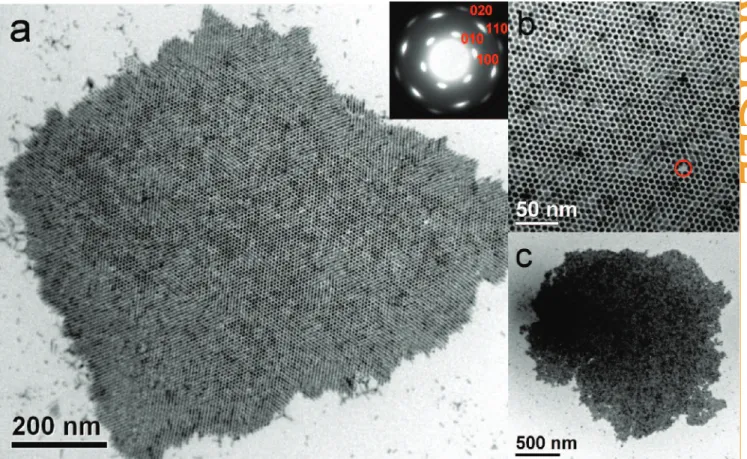
driv-Figure 1. (a) TEM image of TDPA- and TOP-capped CdS nanorods with self-assembled organization in large scale. The inset shows the diffraction pattern of the bundle. (b) TEM image of bundled-up CdS nanorods in higher magnification. (c) An extended TEM image of self-assembled CdS nanorods.
ARTICLE
Downloaded by NATIONAL TAIWAN UNIV on July 27, 2009
ing force. Details of the results and discussion regard-ing the assembled CdS nanorods are elaborated as follows.
RESULTS AND DISCUSSION
Figure 1 panels a and b show TEM images of TDPA and TOP capped, self-assembled CdS nanorods in differ-ent scales. Eviddiffer-ently, as depicted in Figure 1a,b, exclu-sive honeycomb structures were formed. Note that the results are independent of the TEM probing area, as supported by the observation of whole self-bundled CdS nanorods in a largely extended area of microme-ter dimensions depicted in Figure 1c. Because the crys-tal structure of CdS is wurtzite and the growing direc-tion is along the c-axis, nanorods with a hexagonal cross-section are anticipated. The single-crystal-like selective-area diffraction pattern (inset in Figure 1a;
note that the effective aperture size is⬃100 nm and
multiple nanorods in the same domain contribute to the pattern) indicates that in addition to the alignment along the c-axis, the basalplane (a- and b-axis) is also self-aligned. The slightly diffused diffraction spots sug-gest that the basalplane of the rods are rotated within
10°, similar to the results reported by Ryan’s group.31
Note Figure 1b shows nearly perfect 2D assembly, in which only one vacancy in the lower right part (marked by a red circle) is seen from the uniform hexagonal packing of the CdS nanorods perpendicular to the sub-strate. The intriguing issue therefore lies in the reason for the predominant corralling of the nanorods. Accord-ing to previous reports about the self-assembled CdS
superstructure,29–31,34evaporation of the solvent
causes the corralling-together of the nanorods. How-ever, without direction-controlling external
interfer-ence,34the nanorods should form three phases of
pack-ing, namely, smectic, columnar, and crystal, due to the reduction of interfacial energy. Capillary attraction might help the formation of an ordered structure but could not force the nanorods to rearrange normal to the interface. Note that the outer edge of the bundled
structure in Figure 1a shows a slight tilt of the nanorods, being depicted as a columnar
struc-ture,34(also see Figure S-1 in the
Supporting Infromation; the Fou-rier filtered micrograph with en-hanced contrast is presented to view the leaning behavior of edges) the result of which implies that in our experiments,
evaporation-induced corralling of the nanorods might be the origin of the self-assembled CdS super-structure. On the other hand, direction-controlling processes
such as external DC electric field,29
polymer matrix,30and highly
ori-ented pyrolytic carbon31all have the purpose of
orien-tating the nanorods perpendicular to the substrate dur-ing gentle evaporation of solvent. However, these external direction-controlling methods are not used in this study to control the assembly behavior. As a result, besides the evaporation-induced aggregation of the nanorods, we may narrow down the discussion to the following aspects.
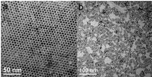
We first consider the concentration effect of the nanorods in the solvent. The sample shown in Figure 1 was prepared with a (toluene) solution that contains 2.5% CdS in weight. With an increase in the weight per-centage from 2.5% to 5%, the same 2D assembly with an area as large as a micrometer dimension was ob-tained (see Figure S-2 in Supporting Information). How-ever, as shown in Figure 2 panels a and b, with a de-crease of the concentration of the CdS nanorods from 2.5 to 0.5 wt %, the 2D framework gradually collapsed.
At a concentration of⬃0.5 wt %, as shown in Figure 2b,
a lying-down monolayer of CdS nanorods with their c-axis parallel to the plane of the grid was clearly ob-served. Therefore, it is reasonable to predict that the critical concentration of the CdS nanorods in toluene for obtaining the assembled structure might be be-tween 0.5% and 2.5% in weight.
Nevertheless, despite the lack of a 2D framework of the CdS nanorods, judging from the TEM image shown in Figure 2b, most of the nanorods are still aligned side by side. The results imply the possible existence of the influence of the surfactants between nanorods, and sur-factants that surround the CdS nanorods might play an important role in the self-bundled superstructure. Initially, the reaction system contains Cd-TDPA com-plex, sulfur, and TOP, among which the surfactants that affect shape and aspect ratios are ascribed to TDPA and TOP. Therefore, interaction between the alkyl groups of surfactants might serve as the direction-controlling agent. The tendency of self-association of the hydrocarbon part on the surfactant is known to be
the driving force for the micelle formation. Wishnia36
Figure 2. TEM image of TDPA- and TOP-capped CdS nanorods with concentrations of (a) 2.5 and (b) 0.5 wt %.
ARTICLE
Downloaded by NATIONAL TAIWAN UNIV on July 27, 2009
has measured the solubility of hydrocarbons such as ethane, propane, butane, and pentane in sodium do-decyl sulfate (SDS) solution and concluded that the hy-drocarbon contribution to the standard free energy is in
the range of⫺12.0RT to ⫺18.2RT. To a certain degree,
the intercrossed hydrocarbon groups of TOP and TDPA that occupy the space between two neighboring CdS nanorods would reduce the free energy and help the self-assembly of CdS nanorods as well. To further mani-fest this viewpoint, we thus measured the surface en-ergy of solutions containing different concentrations of CdS nanorods. As shown in Figure 3, at the interval of CdS nanorod concentration from 0.4 to 1.5 wt %, the surface energy of the solution gradually decreases as the surface concentration of the nanorod increases with the total concentration. Above 1.5 wt %, the surface en-ergy of the solution is independent of the total concen-tration, indicating a constant surface concentration of the nanorod. In other words, the nanorod is saturated in the solution, and aggregates will form to minimize the energy. According to the plot depicted in Figure 3, the critical concentration of the CdS nanorods in tolu-ene should be between 1.0% and 2.0% in weight, in good agreement with the concentration used for the TEM observation of 2D self-bundled CdS nanorods (vide supra). This variation of surface energy supports the fact that upon increasing the concentration of nano-rods in the solution, CdS nanonano-rods saturate and self-assemble into bundles.
Considering a self-assembled monolayer composed of the organic molecules with a headgroup and a long-chain alkane tail on the surface of semiconductor,
Bent37recently concluded that the net result of
compe-tition between intermolecular and interfacial forces tends to alter the behavior of the monolayers. Good alignment of the alkane tails could be achieved in the case if intermolecular forces overcome the
molecule⫺substrate and lattice forces. On the
con-trary, if the interfacial forces appear to dominate over the interchain forces, the head groups form commensu-rate bonding with the underlying surface. Hence,
exten-sively ordered coverage of the head groups on the sur-face causes mismatch between the semiconductor
lattice and molecule⫺molecule spacing among the
head groups. This strain could be released by disorder-ing of the alkane tails, such that the ordered packdisorder-ing of the alkane chains may not be available eventually. These viewpoints further support our observations in the concentration-dependent experiments of the sur-face energy. In other words, after the concentration of CdS nanorods reaches the critical value (0.4 wt %), the intermolecular forces among the alkane-chains of sur-factants on adjacent CdS nanorods surpass the interfa-cial forces between the adsorbed head groups and the surface of the nanorods. Consequently, the construc-tion of self-assembled arrays of CdS nanorods comes with a lowering of surface energy.
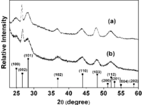
In addition to the solvent-evaporation induced self-assembly, the other key topic would be the direction-controlling effect of the surfactants. We further propose that the three octyl chains from one single TOP mol-ecule might establish a stronger unidirectional super-structure than those surfactants with single hydrocar-bon chains. To verify this hypothesis, we thus tentatively used hexadecylamine (HDA) to substitute part of TOP. Figure 4 shows the X-ray powder diffrac-tion (XRD) patterns of the CdS nanorods prepared by using two sets of surfactants: (a) TDPA and TOP (molar ratio of 1:15) and (b) TDPA, HDA, and TOP (molar ratio of 1:3.5:6, see Experimental Section for details). Both pat-terns show the diffraction peaks matching exactly that of the wurtzite CdS standard pattern (see bottom part of Figure 4). The significantly sharp and narrowed (002)
peak at 26.7 degrees (2) clearly supports the extended
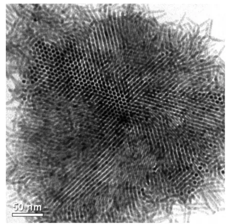
c-axis stacking domain of the wurtzite lattice. Note that the broadening of other peaks is due to the corre-sponding quantized dimensions. Figure 5 shows the TEM image of the CdS nanorods synthesized by using TDPA, HDA, and TOP as surfactants. With control of the concentration of the nanorods (2.0 wt %), self-assembly of the nanorods could also be seen on the carbon-coated copper grid. However, more than half of the nanorods in the bundle leaned on the substrate, even though the crystalline structure (XRD) is identical for Figure 3. The surface energy, measured by pendent drop
method, with respect to different concentrations of CdS nanorods (0, 0.4, 0.8, 1.5, 3.125, and 6.25 wt %).
Figure 4. Powder X-ray diffraction (XRD) of CdS nanorods synthesized by using (a) TDPA and TOP, (b) TDPA, HDA, and TOP, and that of standard CdS (wurtzite) pattern (lower).
ARTICLE
Downloaded by NATIONAL TAIWAN UNIV on July 27, 2009
both cases. Further increase of the concentration of HDA-capped CdS nanorods did not seem helpful for the assembly. Furthermore, upon an increase of the HDA concentration from 1.35 g (used for obtaining Fig-ure 5) to 4.0 g, the percentage of self-bundled CdS na-norods decreased, accompanied by the elongation of CdS nanorods. As a result, types of surfactants should influence the self-assembly. Since a large amount of the TOP was replaced by HDA, the observation of
ran-domly packed bundles suggests that the three octyl groups on the TOP molecule regulate the bundling direction more readily than the single hexadecyl group on the HDA molecule. Moreover, tetradecyl groups on the TDPA might serve as bridges to enhance the corralling structure. Certainly, other mi-nor intrinsic properties of the CdS nami-norods,
such as the dipole⫺dipole interaction and
van der Waals attraction, might also influ-ence the observed self-assembly. As
previ-ously concluded by Korgel and co-workers,33
side-by-side assembly of CdS nanorods was
favored in both dipole⫺dipole interaction
(⬃470 meV or ⬃18kT at room temperature)
and van der Waals attraction (⬃140 meV or
⬃5.4kT) for CdS with an aspect ratio of 9.9. As the emission of quantum confined semiconductors is greatly affected by the di-mensions of the nanocrystals, luminescent properties of the bundled nanorods might differ from those of nanorods in solution. Curve a of Figure 6 shows emission spectra of CdS nanorods synthesized with TDPA and TOP and dispersed in a toluene solution (0.1 wt %). In comparison, curve b is that of a single-bundled array-deposited thin film and measured by a confocal microscope
fo-cused on an array area of 0.5m in diameter using a
GaN laser (406 nm). Clearly, the intensity of the broad emission band from 525 to 700 nm, which arose from defect states of CdS nanorods in solution, decreased significantly when the nanorods were corralled to-gether. This result was also supported by the corre-sponding relaxation dynamics, in which the lifetime of the band-edge emission (monitored at 465 nm) of CdS in toluene solution was measured to be 550 ps. On the other hand, probing the area of the CdS self-bundle ar-ray with confocal microscope revealed that the life-time was as long as 4.5 ns, implying the significant sup-pression of the radiationless quenching processes. Variation of the emission spectra might be due to the great reduction of the lateral surface area in self-bundled arrays. In the CdS bundles, electrons may hop to the neighboring rods, causing the process of recom-bination at the defect states to be quenched. Supple-mentary support of this viewpoint is rendered by tun-ing the GaN laser to the peripheral region (observed with a microscope) of the self-bundle arrays where the assembly is in a relatively loose structure, resulting in an increase in the intensity ratio for CdS versus defect emis-sion (cf. curve c versus curve b). Finally, by redispersing the assembled CdS bundles into toluene, emission of defect states returns to the same magnitude as curve a, demonstrating the physically reversible phenomenon in the self-bundled CdS nanorods.
Figure 5. TEM image of TDPA-, HDA-, and TOP-capped CdS nanorods with concentra-tion of 2.0 wt % (see text for details).
Figure 6. The normalized emission spectra of (a) CdS nanorods (syn-thesized by using TDPA and TOP) solution; (b) peripheral and (c) cen-tral region of a single array in the deposited thin film measured by a confocal microscope. The excitation wavelength is 406 nm (GaN laser) for all measurements.
ARTICLE
Downloaded by NATIONAL TAIWAN UNIV on July 27, 2009
CONCLUSION
In summary, exclusive self-assemblies of TDPA-and TOP-capped CdS nanorods in the absence of ex-ternal direction-controlling processes (e.g., exex-ternal electric field, polymer matrix, or highly oriented py-rolytic carbon) are reported. Combining the results and discussion elaborated above, we thus conclude that by using TDPA and TOP as surfactants, the as-prepared CdS nanorods start to corral together with concentration higher than 2.0% weight percent in toluene. It is believed that the first portion of nano-rods, standing normal to the substrate, serves as a nucleation site. Subsequently, the neighboring nan-orods tend to assemble in the same direction with the assistance of the hydrocarbon chains on
surfac-tants or the interactions among nanorods. The net result is self-assemblies with outer edges of leaning bundles and an inner part of hexagonal packing per-pendicular to the substrate. In comparison to the dominant defect emission of CdS nanorods in tolu-ene solution, the single bundled arrays in a depos-ited thin film a show dramatic decrease of the defect emission, implying the possibilities of enhancing electron transport between nanorods. Accordingly, on the basis of a simple, straightforward bottom-up solution method, it is feasible to construct a mono-layer of nanorod-bundled polarizer with thickness in the dimension of nanometers and area in the dimen-sion of micrometers in an aim to greatly facilitate the future preparation of light-emitting devices.
EXPERIMENTAL SECTION
Tetradecylphosphonic acid (TDPA, 98%) was purchased from Alfa Aesar. Trin-octylphosphine (TOP,⬎85% and
n-hexadecylamine (HDA, 90% were purchased from TCI.
Cad-mium oxide (CdO, 99.99%) and sulfur (S, 99.5%) powder were ob-tained from Strem Chemicals and ACROS, respectively. Chemi-cals were used as received.
CdS nanorods was synthesized according to the literature methods8with modification by varying surfactants. Briefly, a
sul-fur injection solution containing 0.072 g of sulsul-fur (2.25 mmol) was prepared by dissolving sulfur powder in 2 mL of tri-n-octylphosphine. A 0.1 g portion of CdO (0.78 mmol) and 0.4565 g of TDPA (1.64 mmol) were loaded into a 50 mL three-neck flask and heated to 200 °C under Ar flow. After the CdO was com-pletely dissolved, judging by the disappearance of the brown color of CdO, the Cd⫺TDPA complex was allowed to cool to room temperature.
As for the addition of TOP (or HDA), the weight percentage has been optimized such that the formation of the CdS self-bundle array was maximized. In detail, 5 mL of TOP or 1.35 g of HDA was added to the flask, and the temperature was raised to 330 °C to produce an optically clear solution. At this temperature, the sulfur injection solution was swiftly injected into the hot so-lution. The reaction mixture was maintained at 330 °C for growth of CdS crystals. After 5 min, the temperature was quenched to 40 °C to terminate the reaction. Five mL of toluene was then in-troduced to dissolve the reaction mixture, and yellow precipitate was obtained by adding 5 mL of isopropanol, and the mixture was centrifuged at 3000 rpm for 5 min. The precipitate was washed with toluene and isopropanol⫻3 and redispersed in toluene for the TEM characterization. The dried powder of the precipitate was obtained for the XRD measurement. The shapes and size distributions of the nanocrystals were measured with a JEOL JEM 1230 transmission electron microscope (TEM). The sur-face energies of suspensions with different CdS concentrations were determined using the pendant-drop method,35and the
data was analyzed with DataPhysics SCA20 software. The crystal structure and phases of the synthesized samples were analyzed by X-ray powder diffraction (XRD) on a PANalytical X’Pert PRO with Cu K␣ X-ray. Emission spectra were recorded with an Edin-burgh (FS920) fluorometer. To investigate the possible differ-ences in photoluminescence between nanorods in solution and those in self-assembled bundles, the latter were measured with a confocal microscope (WITec AlphaSNOM) coupled with a red-sensitive charge coupled detector (CCD, Princeton Instruments, PI-MAX). Note that in the confocal microscopy, the probing laser (406 nm, 0.3m in diameter) was located on the region of self-assembled bundles determined by TEM. Ti:sapphire laser (Tsu-nami, Spectra-Physics) with an 80 MHz repetition rate was used as the excitation source for the lifetime measurement. This laser beam (820 nm) was directed into a doubling crystal (BBO) to yield an UV beam (406 nm) as a pulsed excitation source for the
solution study. As for the self-bundled CdS nanorods, the 406 nm beam was then guided to a telescope for focusing. The con-focal microscope was applied to monitor the self-bundled CdS nanorods in an area of 0.5m in diameter. The fluorescence sig-nal was asig-nalyzed by the time-correlated single photon count-ing system (SPC-300, Becker & Hickl) and high speed photodetec-tor module (OT900, Edinburgh).
Acknowledgment. We thank the National Science Council,
Tai-wan (No. NSC 96-2120-M-002-007) for financially supporting this research.
Supporting Information Available: Fourier filtered micrograph
with enhanced contrast of the same area in Figure 1a and an ex-tended TEM image of self-assembled CdS nanorods synthesized with TDPA and TOP. This material is available free of charge via the Internet at http://pubs.acs.org.
REFERENCES AND NOTES
1. Peng, X. G.; Manna, L.; Yang, W. D.; Wickham, J.; Scher, E.; Kadavanich, A.; Alivisatos, A. P. Shape Control of CdSe Nanocrystals. Nature 2000, 404, 59–61.
2. Hu, J. T.; Li, L. S.; Yang, W. D.; Manna, L.; Wang, L. W.; Alivisatos, A. P. Linearly Polarized Emission from Colloidal Semiconductor Quantum Rods. Science 2001, 292, 2060–2063.
3. Talapin, D. V.; Koeppe, R.; Gotzinger, S.; Kornowski, A.; Lupton, J. M.; Rogach, A. L.; Benson, O.; Feldmann, J.; Weller, H. Highly Emissive Colloidal CdSe/CdS Heterostructures of Mixed Dimensionality. Nano Lett.
2003, 3, 1677–1681.
4. Hikmet, R. A. M.; Chin, P. T. K.; Talapin, D. V.; Weller, H. Polarized-Light-Emitting Quantum-Rod Diodes. Adv. Mater.
2005, 17, 1436–1439.
5. Acharya, S.; Patla, I.; Kost, J.; Efrima, S.; Golan, V. Switchable Assembly of Ultra Narrow CdS Nanowires and Nanorods.
J. Am. Chem. Soc. 2006, 128, 9294–9295.
6. Manna, L.; Scher, E. C.; Alivisatos, A. P. Synthesis of Soluble and Processable Rod-, Arrow-, Teardrop-, and Tetrapod-Shaped CdSe Nanocrystals. J. Am. Chem. Soc. 2000, 122, 12700–12706.
7. Peng, Z. A.; Peng, X. G. Mechanisms of the Shape Evolution of CdSe Nanocrystals. J. Am. Chem. Soc. 2001,
123, 1389–1395.
8. Peng, Z. A.; Peng, X. G. Formation of Highly-Quality CdTe, CdSe, and CdS Nanocrystals Using CdO as Precursor. J. Am.
Chem. Soc. 2001, 123, 183–184.
9. Jun, Y. W.; Lee, S. M.; Kang, N. J.; Cheon, J. W. Controlled Synthesis of Multi-armed CdS Nanorod Architectures Using Monosurfactant System. J. Am. Chem. Soc. 2001, 123, 5150–5151.
ARTICLE
Downloaded by NATIONAL TAIWAN UNIV on July 27, 2009
10. Li, L. S.; Hu, J. T.; Yang, W. D.; Alivisatos, A. P. Band Gap Variation of Size- and Shape-Controlled Colloidal CdSe Quantum Rods. Nano Lett. 2001, 1, 349–351.
11. Qu, L. H.; Peng, Z. A.; Peng, X. G. Alternative Routes toward High Quality CdSe Nanocrystals. Nano Lett. 2001, 1, 333– 337.
12. Qu, L. H.; Peng, X. G. Control of Photoluminescence Properties of CdSe Nanocrystals in Growth. J. Am. Chem.
Soc. 2002, 124, 2049–2055.
13. Peng, Z. A.; Peng, X. G. Nearly Monodisperse and Shape-Controlled CdSe Nanocrystals via Alternative Routes: Nucleation and Growth. J. Am. Chem. Soc. 2002, 124, 3343– 3353.
14. Manna, L.; Scher, E. C.; Li, L. S.; Alivisatos, A. P. Epitaxial Growth and Photochemical Annealing of Graded CdS/ZnS Shells on Colloidal CdSe Nanorods. J. Am. Chem. Soc. 2002,
124, 7136–7145.
15. Yu, W. W.; Peng, X. G. Formation of High-Quality CdS and Other II-VI Semiconductor Nanocrystals in
Noncoordinating Solvents: Tunable Reactivity of Monomers. Angew. Chem., Int. Ed. 2002, 41, 2368–2371. 16. Peng, X. G. Mechanisms for the Control and
Shape-Evolution of Colloidal Semiconductor Nanocrystals. Adv.
Mater. 2003, 15, 459–463.
17. Mokari, T.; Banin, U. Synthesis and Properties of CdSe/ZnS Core/Shell Nanorods. Chem. Mater. 2003, 15, 3955–3960. 18. Yu, W. W.; Wang, Y. A.; Peng, X. G. Formation and Stability
of Size-, Shape-, and Structure-Controlled CdTe Nanocrystals: Ligand Effects on Monomers and Nanocrystals. Chem. Mater. 2003, 15, 4300–4308. 19. Milliron, D. J.; Hughes, S. M.; Cui, Y.; Manna, L.; Li, J.; Wang,
L. W.; Alivisatos, A. P. Colloidal Nanocrystal
Heterostructures with Linear and Branched Topology.
Nature 2004, 430, 190–195.
20. Qu, L. H.; Yu, W. W.; Peng, X. G. In Situ Observation of the Nucleation and Growth of CdSe Nanocrystals. Nano Lett.
2004, 4, 465–469.
21. Shieh, F.; Saunders, A. E.; Korgel, B. A. General Shape Control of Colloidal CdS, CdSe, CdTe Quantum Rods and Quantum Rod Heterostructures. J. Phys. Chem. B 2005, 109, 8538–8542.
22. Kumar, S.; Nann, T. Shape Control of II-VI Semiconductor Nanomaterials. Small 2006, 2, 316–329.
23. Gur, I.; Fromer, N. A.; Geier, M. L.; Alivisatos, A. P. Air-Stable All-Inorganic Nanocrystal Solar Cells Processed from Solution. Science 2005, 310, 462–464.
24. Huynh, W. U.; Dittmer, J. J.; Alivisatos, A. P. Hybrid Nanorod-Polymer Solar Cells. Science 2002, 295, 2425–2427.
25. Qnsager, L. The Effects of Shape on the Interaction of Colloidal Particles. Ann. N. Y. Sci. 1949, 51, 627–659. 26. Li, L. S.; Walda, J.; Manna, L.; Alivisatos, A. P.
Semiconductor Nanorod Liquid Crystals. Nano Lett. 2002,
2, 557–560.
27. Li, L. S.; Alivisatos, A. P. Semiconductor Nanorod Liquid Crystals and Their Assembly on a Substrate. Adv. Mater.
2003, 15, 408–411.
28. Talapin, D. V.; Shevchenko, E. V.; Mirry, C. B.; Kornowski, A; Forster, S.; Weller, H. CdSe and CdSe/CdS Nanorod Solids.
J. Am. Chem. Soc. 2004, 126, 12984–12988.
29. Ryan, K. M.; Mastroianni, A.; Stancil, K. A.; Liu, H. T; Alivisatos, A. P. Electric-Field-Assisted Assembly of Perpendicularly Oriented Nanorod Superlattices. Nano
Lett. 2006, 6, 1479–1482.
30. Gupta, S.; Zhang, Q. L.; Emrick, T.; Russell, T. P. “Self-Corralling” Nanorods under an Applied Electric Field. Nano
Lett. 2006, 6, 2066–2069.
31. Ahmed, S.; Ryan, K. M. Self-Assembly of Vertically Aligned nanorod Supercrystals Using Highly Oriented Pyrolytic Graphite. Nano Lett. 2007, 7, 2480–2485.
32. Carbone, L.; Nobile, C.; Giorgi, M. D.; Sala, F. D.; Morello, G. Pompa, P.; Hytch, M.; Snoeck, E.; Fiore, A.; Franchini, I. R.; et
al. Synthesis and Micrometer-Scale Assembly of Colloidal
CdSe/CdS Nanorods Prepared by a Seeded Growth Approach. Nano Lett. 2007, 7, 2942–2950.
33. Ghezelbash, A.; Koo, B.; Korgel, B. A. Self-Assembled Stripe Patterns of CdS Nanorods. Nano Lett. 2006, 6, 1832–1836.
34. He, J.; Zhang, Q. L.; Gupta, S; Emrick, T.; Russell, T. P.; Thiyagarajan, P. Drying Droplets: A Window into the Behavior of Nanorods at Interface. Small 2007, 3, 1214–1217.
35. Winkel, D. Theoretical Refinement of the Pendant Drop Method for Measuring Surface Tensions. J. Phys. Chem.
1965, 69, 348–350.
36. Wishnia, A. The Hydrophobic Contribution to Micelle Formation: The Solubility of Ethane, Propane, Butane, and Pentane in Sodium Dodecyl Sulfate Solution. J. Phys. Chem.
1963, 67, 2079–2082.
37. Bent, S. F. The Hydrophobic Contribution to Micelle Formation: The Solubility of Ethane, Propane, Butane, and Pentane in Sodium Dodecyl Sulfate Solution. ACS Nano
2007, 1, 10–12.
ARTICLE
Downloaded by NATIONAL TAIWAN UNIV on July 27, 2009