行政院國家科學委員會專題研究計畫 成果報告
子計畫二:奈米粒子與光學晶體上之光電元件製作和研究
(2/2)
計畫類別: 整合型計畫 計畫編號: NSC92-2120-E-002-003- 執行期間: 92 年 08 月 01 日至 93 年 07 月 31 日 執行單位: 國立臺灣大學光電工程學研究所 計畫主持人: 林清富 計畫參與人員: 孫國瑞、李俊育、黃耀德、趙家忻 報告類型: 完整報告 處理方式: 本計畫可公開查詢中 華 民 國 93 年 12 月 17 日
行政院國家科學委員會專題研究計畫成果報告
奈米粒子與光學晶體上之光電元件製作與研究 (2/2)
Fabrication and investigation of optoelectronic devices based on
nano-particles and photonic crystals
計畫編號:NSC 92-2120-E-002-003
執行期限:92 年 8 月 1 日至 93 年 7 月 31 日
主持人:林清富 台灣大學光電工程研究所
一、 中文摘要在今年度的研究中,我們成功製作出將氧化鉺 (erbium oxide)與氧化磷 (phosphorous oxide)混合旋塗玻璃 (spin-on glass) 溶液,佈塗在矽基板 (silicon substrate)上,製作簡單 且低成本的發光層,發射波長在光通訊使用的 1530 nm。
關鍵詞:奈米科技、光通訊、稀土元素、氧化鉺、氧化磷。 英文摘要
We introduce a new manufacturing technique that lays a light emitting layer on silicon wafer. This layer is formed with the mixture of Er2O3 nanoparticles and spin-on glass. It emits 1530nm light because Er2O3 releases Er3+ at high temperature. The process is simple. We also add P2O5, Al and Ag nanoparticles to improve light emission.
Key words: Nanotechnology, optical communication, optical pumping, rare earth
compounds.
二、前言與研究目的
The amount of data transmission continues to grow, so the advantage of high transmission capability of optical fiber is of great worth. The demand for optical components also rockets up. Erbium-doped optical fiber amplifier is the core technique of modern optical communication systems. However, erbium-doped optical fiber has several disadvantages. For example, it has expensive fabricating cost. In addition, it is difficult to monolithically integrate with electronics. Thus, we introduce a new manufacturing technique to create a light emitting layer on Si wafer. It emits light at 1530nm. The fabrication process is very simple and nearly costless, compared with ion implantation technique. In addition, it can be possibly
integration. Moreover, we can extend the applications of Si such as taking the Si optoelectronic integrated circuits (OEIC) for the light source of optical communication systems.
三、文獻探討
Erbium doped fiber is the cone technology of modern optical communication systems [1]. Semiconductor manufacturing processes have been extensively studied [2]. With different nanoparticles size, quantum size effect on optical properties can be observed [2]. Different co-dopant can change the property of erbium doped fiber [3-7]. In this work, optical pumping and photoluminescence of emitting layer of Er2O3 nanoparticles are demonstrated. It was found Al2O3 improves fluorescent lifetime of Er3+ ions, but the integrated absorption cross-section of Er3+ ions decreases with the increase of Al2O3 concentration [8].
四、研究方法
1. Preparation of emitting layer
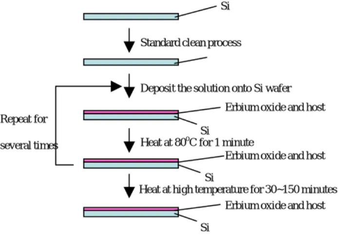
The manufacturing process is schematically shown in Fig.1. A piece of silicon wafer is cleaned with standard procedure. Er2O3, P2O5, Al and Ag nano-particles are mixed into spin-on glass (SOG), which is taken as the host material. The Er2O3 nanoparticles are uniformly distributed in the solution. Then, we deposit the solution on the silicon wafer and soft bake in 80oC for 1 minute. Repeat this step for a few times to obtain a thick emitting layer. In the final step, heat the sample in 880oC~1000oC for 30~150 minutes in order to make the Er2O3 release Er3+ and react with SOG. The heating temperature has to be 880oC or above so that Er2O3 would be reactive.
We also used high energy ultraviolet laser to anneal the samples. The energy is so high that the Si substrate could be melted and then re-crystallizes. This post heat treatment can help the emitting layer gets more uniform and promote the light emission efficiency.
Though, we have to make some compromise. If the energy density is high, the emitting would be spluttered. Therefore, we lower the energy density to avoid the phenomenon, and have Er3+ better bounded with glass structure in the emitting layer.
A large Er3+ doping concentration in silica glass results in concentration quenching caused by ion clusters. Phosphate and silicate glasses are superior to silica glass for the realization of high concentration erbium-doped optical amplifiers.
Due to the high solubility of rare-earth ions without cluster formation, phosphate glasses are of great interest as a gain medium for compact erbium-doped optical amplifiers. Therefore, we add P2O5 nanoparticlesto the solution of light emitting layer to reduce cluster formation.
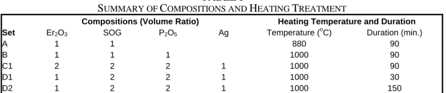
The different sets of Er2O3, P2O5, and Ag mixture with different volume ratio were experimented. The different compositions result in samples with variable properties, such as conductivity and formation of cluster. Table I lists these different compositions.
2. Photoluminescence setup
Fig.2 shows the measurement setup. Take 980nm laser diode as pumping source, and focus it on the sample after a collimator and a mirror. InGaAs detector receives the light emitted by the sample through two lenses and CM110 monochromater. Finally, lock-in amplifier SRS SR830 that is triggered by optical chopper MC1000 amplifies the signals from detector, and transfers the amplified signals to the computer. Following measurements of photoluminescence are under optimized alignment.
3. Setup of measuring optical gain
Fig. 8 illustrates the setup of optical gain measurement. The specimen is pumped with the 980 nm laser diode because Er3+ has strong absorption around this wavelength. Pumping light emitted out from the laser diode is collimated by the first lens. Afterwards, it is re-focused by the cylindrical lens and shaped into a narrow light stripe. This light stripe is cast onto the specimen with a movable block placed in front of it. We can change the length of the pumping stripe on specimen by moving the block. To prevent the pumping source (980 nm) entering the monochromator, a low pass filter is set in front of the monochromator. The measurements of photoluminescence are done with optimized alignment.
TABLE I
SUMMARY OF COMPOSITIONS AND HEATING TREATMENT
Compositions (Volume Ratio) Heating Temperature and Duration
Set Er2O3 SOG P2O5 Ag Temperature (oC) Duration (min.)
A 1 1 880 90
B 1 1 1 1000 90
C1 2 2 2 1 1000 90
D1 1 2 2 1 1000 30
五、結果與討論
A. Er2O3, and SOG Only
In Set A, only Er2O3 and SOG were mixed. Although the compositions are quite simple, there is already an emitting peak at 1530nm (Fig. 3).
B. Effect of P2O5 and Ag Nanoparticles
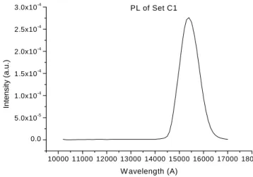
The effect of P2O5 and Ag nanoparticles was investigated with samples prepared using a similar procedure (Fig. 1). We added P2O5 nanoparticles to the solution of Set B, and Ag nanoparticles to the solution of Set C1. Fig. 3 illustrates the photoluminescence spectra of Set A and Set B. Fig. 4 illustrates the photoluminescence spectrum of Set C1. These samples have different physical properties and all of them emit light at 1530nm with different light emission characteristics of spectrum. Set C1 shows highest signal level among all the sets. Although it has quite high signal level, the layer of sample C1 is somehow badly uniform.
The original motivation of adding Ag nanoparticles to the solution of the emitting layer is to improve conductivity. However, we discovered an extra benefit of increasing light emission efficiency. Fig. 4 illustrates the high peak intensity of photoluminescence for the sample with the Ag nanoparticles (Set C1). To explain this phenomenon, we presume that Ag atoms play the role that transfers energy to Er3+ by free carrier absorption. Therefore, Er3+ ions are more easily to be excited for efficiency increase.
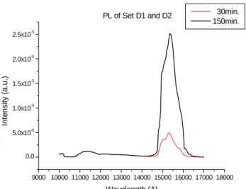
C. Effect of Heating Duration
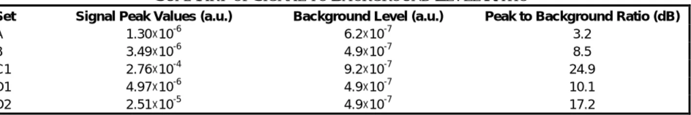
To reveal the effect of heating duration, we compare the difference between set D1 and set D2, which was heated for 30 and 150 minutes respectively. Their manufacturing processes are the same as other samples (Fig. 1), and compositions are listed in TABLE I. Fig. 5 shows the photoluminescence for Set D1 and Set D2. The comparison between D1 and D2 shows that samples with a longer heating duration (D2) have more emission than samples with a shorter heating duration (D1). Their signal to background level ratio is listed in TABLE II.
The heat treatment is also an important parameter of the experiment. In our experiment, samples without heat treatment of high temperature cannot emit light around 1530nm because
TABLE II
SUMMARY OF SIGNAL TO BACKGROUND LEVEL RATIO
Set Signal Peak Values (a.u.) Background Level (a.u.) Peak to Background Ratio (dB)
A 1.30×10⁻⁶ 6.2×10⁻⁷ 3.2
B 3.49×10⁻⁶ 4.9×10⁻⁷ 8.5
C1 2.76×10⁻⁴ 9.2×10⁻⁷ 24.9
D1 4.97×10⁻⁶ 4.9×10⁻⁷ 10.1
Er2O3 is inertial below 880oC. Experiments show that light emission increases with the heating duration (Fig. 5). The peak intensity of Set D2 is about five times than peak intensity of Set D1.
D. Effect of Al Nanoparticles
The samples with Al nanoparticles are also prepared. Fig. 6 is PL spectrum with the sample pumped by different pumping power. It shows relatively high signal level (13.7dB) and smooth spectrum curves. Al nanoparticles are possibly oxidized to form Al2O3 in the heating process and it has been known that Al2O3 can improve the solubility of rare earth ions.
Ordinary erbium-doped optical fiber requires a quite long distance to acquire significant light emission from Er3+ ions. Relatively, our emitting layer is able to show the signals only within 0.5µm due to the higher concentration of Er3+ and surface effect of nano-particles.
It was found Al2O3 improves fluorescent lifetime of Er3+ ions, but the integrated absorption cross-section of Er3+ ions decreases with the increase of Al2O3 concentration. Lower Al2O3 content, and 0.2–0.4 mol% Er2O3 are preferred for LD pumped microchip laser application. OH groups in glass greatly affect fluorescent intensity and lifetime of Er3+. [8]
D. Effect of Si Nanoparticles
A large Er3+ doping concentration in silica glass results in concentration quenching caused by ion clusters. Phosphate and silicate glasses are superior to silica glass for the realization of high concentration erbium-doped optical amplifiers [2]. Therefore, P2O5 nanoparticles are added to the solution of light emitting layer to reduce cluster formation. According to our experiments, the heating temperature and duration are important parameters. Si nanoparticles could also improve the emission at 1530 nm by 47% (Fig. 7). Si nanoparticles play the role that absorb energy form 980 nm pumping source and transfer energy to Er3+, so the emission efficiency is increased.
E. Observation of Optical Gain
The signal at 1530 nm is observed to super-linearly proportional to the pumping length, while the pumping power is linearly proportional to the pumping length, as show in Fig. 9. This is evidence that the emitting layer reveals optical gain.
六、計畫結果自評
Emitting 1530nm light on Si wafer is very useful because 1530nm is an important band in optical fiber communication. We demonstrated a simple process to form light-emitting layer
on Si. The properties of samples can be varied through controlling the composition. A very valuable part of the process is that it can be possibly integrated with IC manufacturing process. In the future, building electrical and optical systems together on Si will be an expected achievement.
七、參考資料
[1] Michel J. F. Digonnet, Rare Earth Doped Fiber Lasers and Ampilifers, Dekker, 1993
[2] Xiao, Intooduction to Semiconductor Manufacturing Technology, Prentice Hall, 2001
[3] William J. Miniscalco, “Erbium-Doped Glasses for Fiber Amplifiers at 1500 nm” Journal of Lightwave Technology, Vol. 9, No. 2, February 1991.
[4] Emmanuel Desurvire, Erbium-doped Fiber Amplifiers, John Wiley & Sons, 1994
[5] P.W. France, Optical Fiber Lasers and Amplifiers, Blackie, 1991
[6] S. Kennou, S. Ladas, M. G. Grimaldi, T. A. Nguyen Tan, J. Y. Veuillen, “Oxidation of thin erbium and erbium silicide overlayers in contact with silicon oxide films thermally grown on silicon” Applied Surface Science, 102, pp. 142-146, 1996.
[7] Karine Seneschal, Frederic Smektala, Shibin Jiang, Tao Luo, Bruno Bureau, Jacques Lucas, Nasser Peyghambarian, “Alkaline-free phosphate glasses for ultra compact opticalfiber amplifiers at 1.5 µm” Journal of Non-Crystalline Solids, 324, pp. 179-186, 2003.
[8] Zhuping Liu, Changhong Qi, Shixun Dai, Yasi Jiang, Lili Hu, “Spectra and laser properties of Er3+, Yb3+:phosphate glasses” Optical Materials, 21, pp. 789–794, 2003 八、圖表
Fig. 1: Sample manufacturing process.
Standard clean process
Deposit the solution onto Si wafer
Heat at 80oC for 1 minute
Repeat for several times
Heat at high temperature for 30~150 minutes Si
Erbium oxide and host
Si
Erbium oxide and host
Si
Erbium oxide and host Si
Fig. 2: Photoluminescence measurement setup 9000 10000 11000 12000 13000 14000 15000 16000 17000 18000 0.0 5.0x10⁻⁷ 1.0x10⁻⁶ 1.5x10⁻⁶ 2.0x10⁻⁶ 2.5x10⁻⁶ 3.0x10⁻⁶ 3.5x10⁻⁶
PL of Set A and Set B
In te n s it y ( a .u .) Wavelength (A) Set A Set B
Fig. 3: Photoluminescence spectrum of Set A and B.
10000 11000 12000 13000 14000 15000 16000 17000 18000 0.0 5.0x10⁻⁵ 1.0x10⁻⁴ 1.5x10⁻⁴ 2.0x10⁻⁴ 2.5x10⁻⁴ 3.0x10⁻⁴ PL of Set C1 Inte ns it y ( a .u.) W avelength (A)
9000 10000 11000 12000 13000 14000 15000 16000 17000 18000 0.0 5.0x10⁻⁶ 1.0x10⁻⁵ 1.5x10⁻⁵ 2.0x10⁻⁵ 2.5x10⁻⁵ PL of Set D1 and D2 In tensi ty ( a .u .) Wavelength (A) 30min. 150min.
Fig. 5: Photoluminescence spectra of Set D1 and D2 show the effect of heating duration.
1300 1350 1400 1450 1500 1550 1600 0.0 5.0x10⁻⁶ 1.0x10⁻⁵ 1.5x10⁻⁵ 2.0x10⁻⁵ 2.5x10⁻⁵ 3.0x10⁻⁵ Weight Ratio Er2O3 : P2O5 : Al : SOG#315F = 0.26 : 0.12 : 0.01 : 1.06 Heated with N2=100sccm Int e ns ity (a.u.) Wavelength (nm) Laser Diode Pumping Current
200mA 400mA 700mA
Fig. 6: Photoluminescence spectra of sample with Al nanoparticles under different pumping power
900 1000 1100 1200 1300 1400 1500 1600 1700 0.0 0.2 0.4 0.6 0.8 1.0 Inte n s ity ( a .u.) Wavelength (nm) S040805A1 Er2O3-11.7% P2O5-6.4% SOG-81.9% S040805B1 Er2O3-11.0% P2O5-6.2% Si-0.8% SOG-82.0%
Fig. 8. Setup of measuring optical gain 9.5 10.0 10.5 11.0 11.5 12.0 12.5 10 20 30 40 50 60 P L In te n s it y ( a .u .) Er 2O3 : P2O5 : P104F = 1: 0.56 : 4.02 30 min @ 300oC 90min@1000oC Pumping Power at 700mA
P u mpi ng P o w e r ( m W )
Relative Pumping Length (mm)
86.0 86.2 86.4 86.6 86.8 87.0 87.2 87.4 87.6 87.8 88.0 88.2 88.4 88.6 88.8 89.0 89.2 89.4 040912A PL Intensity
Fig. 9 The pumping power at 980 nm and the optical signal at 1530 nm vs. pumping length.
980 nm laser
Monochromator
Detector Lock-in Computer
Chopper
Low pass filter Cylindrical lens
Lens
Si substrate with