國
立
交
通
大
學
資訊學院 資訊學程
碩
士
論
文
運用非同步電路設計之快速傅立葉轉換處理器
The Design of Asynchronous FFT Processor
研 究 生:劉建春
指導教授:陳昌居 教授
中 華 民 國 九 十 八 年 七 月
運用非同步電路設計之快速傅立葉轉換處理器
The Design of Asynchronous FFT Processor
研 究 生:劉建春 Student:Jian-Chun Liu
指導教授:陳昌居 教授 Advisor:Dr. Chang-Jiu Chen
國 立 交 通 大 學
資訊學院 資訊學程
碩 士 論 文
A Thesis
Submitted to College of Computer Science National Chiao Tung University in Partial Fulfillment of the Requirements
for the Degree of Master of Science
in
Computer Science July 2009
運用非同步電路設計之快速傅立葉轉換處理器
研究生:劉建春
指導教授:陳昌居 教授
國 立 交 通 大 學
資 訊 學 院 資 訊 學 程 碩 士 班
摘 要
快速傅立葉轉換處理器(FFT Processor)應用在非常多的領域,例如正交分頻多工 Orthogonal Frequency-Division Multiplexing(OFDM) 系 統 、 數 位 訊 號 處 理 Digital Signal Process(DSP)模組、網路資料傳輸(WLAN、xDSL、WiMAX、Wireless)、數位影像 處 理 (Image Processing Technique) 、 高 畫 質 電 視 地 面 廣 播 High-Definition Television(HDTV) 、 MP3 編 碼 器 / 解 碼 器 (Encoder/Decoder) 、 頻 譜 分 析 (Spectrum Analysis) ...等等。在這篇論文裡,我們運用非同步電路設計的方式,來簡化傳統同步電路傅立葉轉換 處理器的設計;去除在同步電路設計時,需考慮時脈偏斜(clock-skew)、時脈分佈以及 時脈頻率最壞情況估算的煩惱;盡量減少乘法運算、並以非同步管線之控制電路來增加 效能。用此方式設計,在電壓、溫度以及運行處理參數上,具有較佳的環境抗逆性。
The Design of Asynchronous FFT Processor
Student:Jian-Chun Liu
Advisor:Dr. Chang-Jiu Chen
Degree Program of Computer Science
National Chiao Tung University
Abstract
The Fast Fourier Transform (FFT) processor has been widely applied for many applications, such as Orthogonal Frequency-Division Multiplexing (OFDM) Systems, Digital Signal Process (DSP) modules, Network Data Transmission (WLAN, xDSL, WiMAX, Wireless), Imaging Processing Technique, High-Definition Television (HDTV), MP3 Encoder/Decoder and Spectrum Analysis … etc.
In this thesis, we apply the design of asynchronous circuit to simplify the conventional synchronous circuit of FFT processor. It stays away from worries that caused by clock-skew, clock-distribution and clock-rate worst-case estimation of synchronous circuit design It also reduce the computation of multiplier, and improve the performance by asynchronous pipeline control circuit. This design is tolerant to variations in supply voltage, temperature and fabrication process parameters.
Acknowledgement
首先,要非常感謝指導教授 陳昌居 博士 這兩年多來的細心教導,以及口試委 員們的寶貴意見;還要感謝博士班緯民、元騰以及宏岳學長在電路設計、論文研究上 提供非常多珍貴的經驗,加上我們歷屆交大資工計算機實驗室同學們(嘉承、俊瑋、俊 智、榮祥…等)的共同研究,讓我這些年受益良多。以及感謝職場上的同事與摯友們(永 文、榮華、永中、家顯、建立…等),常在忙得不可開交的時候伸出援手。最重要的是 感謝親愛的家人,無時無刻的鼓勵我。 感謝您們大家的幫忙。謝謝大家。感恩。 劉建春 謹識CONTENTS
摘 要 ... I
ABSTRACT ...II ACKNOWLEDGEMENT ... III CONTENTS ... IV LIST OF FIGURES... VII LIST OF TABLES... IX
CHAPTER 1 INTRODUCTION... 1
1.1MOTIVATION...1
1.2THE PROS AND CONS OF ASYNCHRONOUS CIRCUIT DESIGN...2
1.2.1 Advantage of Asynchronous Circuit Design ... 2
1.2.2 Disadvantage of Asynchronous Circuit Design ... 3
1.3ORGANIZATION OF THIS THESIS...4
CHAPTER 2 RELATED WORKS ... 5
2.1EXISTING FFTPROCESSORS...5
2.2SYNCHRONOUS VS.ASYNCHRONOUS...5
2.3ASYNCHRONOUS CIRCUIT DESIGN CONCEPTS...6
2.3.1 Handshake Protocols... 6
2.3.2 Asynchronous encoding ... 7
3.3THE FFT ALGORITHM...14
3.4THE RADIX-2DIT/DIFFFT... 14
3.4.1 The Radix-2 FFT (DIT Version) ... 14
3.4.2 The Radix-2 FFT (DIF Version) ... 19
3.5OTHER FFT ALGORITHMS...22
CHAPTER 4 FFT PROCESSOR ARCHITECTURE ... 23
4.1FFTPROCESSOR ARCHITECTURE...23
4.2COLUMN FFTPROCESSOR...23
4.3PIPELINED FFTPROCESSORS...24
4.3.1 MDC (Multi-path Delay Commutator) ... 25
4.3.2 SDF (Single-path Delay Feedback) ... 26
4.4COMPARISON OF PIPELINED FFTPROCESSORS...27
CHAPTER 5 DESIGN AND IMPLEMENTATION ... 29
5.1C-ELEMENT...29
5.2 ASYNCHRONOUS PIPELINE...32
5.2.1 coarse-grain and fine-grain pipeline ... 32
5.2.2 Muller pipeline... 33
5.2.3 4-phase bundled-data pipeline ... 33
5.2.4 2-phase bundled-data pipeline (Micropipelines) ... 34
5.2.5 4-phase dual-rail pipeline... 36
5.3 8-POINTS RADIX-2DIFFFT WITH SDF STRUCTURE...36
5.3.1 Data flow ... 36
5.3.2 Butterfly units ... 40
5.4 IMPLEMENTATION OF 4-PHASE DUAL-RAIL ASYNCHRONOUS CIRCUIT...41
5.4.2 4-phase dual-rail OR gate ... 43
5.4.3 4-phase dual-rail JOIN, FORK... 44
5.4.4 4-phase dual-rail MERGE ... 45
5.4.5 Completion Detection ... 47
5.4.6 4-phase dual-rail Full Adder / Subtracter ... 48
5.4.7 4-phase dual-rail DEMUX / MUX ... 50
5.5 IMPLEMENTATION OF TWIDDLE FACTOR...53
5.6 RADIX-2DIFSDFFFTSTAGE SCHEMATIC...54
5.7 THE SIMULATION RESULT...56
5.8 THE AREA REPORT...57
5.9THE POWER CONSUMPTION REPORT...58
CHAPTER 6 CONCLUSIONS AND FUTURE WORKS... 59
List of Figures
FIGURE 1:BLOCK DIAGRAM OF AN OFDM SYSTEM USING IFFT/FFTPROCESSOR...1
FIGURE 2:SYNCHRONOUS AND ASYNCHRONOUS COMMUNICATION...6
FIGURE 3: HANDSHAKE PROTOCOL (A)4-PHASE BUNDLED-DATA (B)2-PHASE BUNDLED-DATA...7
FIGURE 4:BUNDLED-DATA ENCODING...8
FIGURE 5:4-PHASE DUAL-RAIL PROTOCOL...8
FIGURE 6:2-PHASE DUAL-RAIL PROTOCOL...8
FIGURE 7:1-OF-4 ENCODING...9
FIGURE 8:A CIRCUIT FRAGMENT WITH GATE DELAYS AND WIRE DELAYS...10
FIGURE 9:THE CLASSIFICATION BASED ON DELAY MODEL... 11
FIGURE 10:PARTIAL TWIDDLE FACTOR OF AN N-POINT DFT ... 13
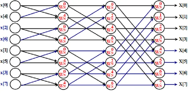
FIGURE 11:8-POINTS RADIX-2DITFFT(N=8)... 16
FIGURE 12:8-POINTS RADIX-2DITFFT(N=8) WITH DECOMPOSED 2 TIMES...17
FIGURE 13:8-POINTS RADIX-2DITFFT(N=8) WITH DECOMPOSED 3 TIMES...18
FIGURE 14:BASIC RADIX-2DITFFTBUTTERFLY UNIT...18
FIGURE 15:SFG OF 8-POINTS RADIX-2DITFFT(N=8)... 19
FIGURE 16:8-POINTS RADIX-2DIFFFT(N=8)... 21
FIGURE 17:SFG OF 8-POINTS RADIX-2DIFFFT(N=8) AFTER SIMPLIFYING...21
FIGURE 18:BASIC RADIX-2DIFFFTBUTTERFLY UNIT...22
FIGURE 19:COLUMN MAJOR FFT ARCHITECTURE (DIT) ... 24
FIGURE 20:ROW MAJOR FFT(DIF) ... 24
FIGURE 21:8-POINTS RADIX-2DIFFFTPROCESSOR WITH MDC STRUCTURE...25
FIGURE 22:GENERAL R2MDC STRUCTURE...25
FIGURE 24:GENERAL R2SDF STRUCTURE...27
FIGURE 25:C-ELEMENT (A) SYMBOL (2)GATE-LEVEL (3) WAVE FORM...30
FIGURE 26:C-ELEMENT WITH DYNAMIC CMOS... 31
FIGURE 27:C-ELEMENT WITH STATIC CMOS ... 31
FIGURE 28: COARSE-GRAIN AND FINE-GRAIN PIPELINE...32
FIGURE 29:THE MULLER PIPELINE...33
FIGURE 30:4-PHASE BUNDLED-DATA PIPELINE...34
FIGURE 31:2-PHASE BUNDLED-DATA PIPELINE (MICROPIPELINES)... 35
FIGURE 32:4-PHASE DUAL-RAIL PIPELINE...36
FIGURE 33:DATA FLOW OF 8-POINTS RADIX-2DIFFFT WITH SDF STRUCTURE...40
FIGURE 34:TWO OPERATION MODES OF R2SDFBUTTERFLY UNITS...40
FIGURE 35:4-PHASE DUAL-RAIL AND GATE...42
FIGURE 36:4-PHASE DUAL-RAIL OR GATE...43
FIGURE 37:4-PHASE DUAL-RAIL JOIN... 44
FIGURE 38:4-PHASE DUAL-RAIL FORK... 44
FIGURE 39:4-PHASE DUAL-RAIL MERGE CIRCUIT...46
FIGURE 40:16-BITS 4-PHASE DUAL-RAIL MERGE CIRCUIT...46
FIGURE 41:N-BITS COMPLETION DETECTION CIRCUIT...47
FIGURE 42:4-PHASE DUAL-RAIL FULL ADDER...49
FIGURE 43:4-PHASE DUAL-RAIL SUBTRACTER...50
FIGURE 44:4-PHASE DUAL-RAIL DEMUX CIRCUIT AND WAVE FORM...51
FIGURE 45:4-PHASE DUAL-RAIL MUX CIRCUIT AND WAVE FORM...52
L
IST OF
T
ABLES
TABLE 1:CLASSIFICATION OF ASYNCHRONOUS CIRCUIT... 11
TABLE 2:COMPARISON OF MDC AND SDF... 27
TABLE 3:COMPARISON OF PIPELINED FFTPROCESSORS...28
TABLE 4:TRUTH TABLE OF C-ELEMENT...29
TABLE 5:TRUTH TABLE OF 4-PHASE DUAL-RAIL MERGE ... 45
TABLE 6:FULL ADDER TRUTH TABLE...48
TABLE 7:4-PHASE DUAL-RAIL DEMUX... 51
TABLE 8:THE AREA REPORT OF RELATED ELEMENTS...57
TABLE 9:THE AREA REPORT OF PROPOSED FFT PROCESSOR...58
Chapter 1 Introduction
The goal of this thesis is to elaborate the concept of design and implementation of FFT Processor with asynchronous circuit. In this chapter, we describe the motivation of the design of asynchronous FFT processor. Section 2 introduces the advantages and disadvantages of asynchronous circuit design. In section 3, we describe the organization of this thesis.
1.1 Motivation
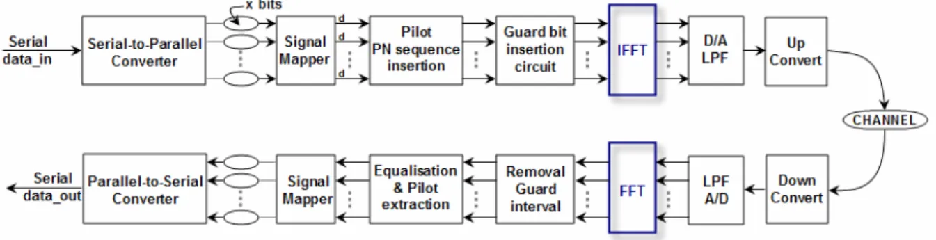
The Fast Fourier Transform (FFT) is an algorithm that effectively computes the Discrete Fourier Transform (DFT). The FFT processor has been widely used for a lot of applications such as OFDM system, Digital Signal Processing (DSP), network transformation, spectrum analysis, imaging processing … etc. [1] for a long time. The following figure is an example of OFDM system using IFFT/FFT processor.
Figure 1 : Block diagram of an OFDM system using IFFT/FFT Processor
deal of care is needed in the design of the “Clock Distribution Networks”. In synchronous circuit designs, clock-skew (also called “timing-skew”) is a phenomenon in synchronous circuits in which the clock signal (sent from the clock circuit) arrives at different components at different time. This would be caused by many different things, such as wire-interconnect length, temperature variations, variation in intermediate devices, capacitive coupling, material imperfections, and differences in input capacitance on the clock inputs of devices using the clock. As the clock rate of a circuit increases, timing becomes more critical and less variation can be tolerated if the circuit is to function properly.
Relatively, in asynchronous circuit design, there is no global signal that needs to be distributed with minimal phase skew across circuits. It inherently avoids the clock-skew problem (because of no clock). The next section introduces the advantages and disadvantages of asynchronous circuit design.
1.2 The Pros and Cons of Asynchronous Circuit Design
To comprehend the system of asynchronous circuit design, it states in terms of internal and external events. These “events” are signal transitions. It uses handshake protocols between system components to ensure correct sequencing of signal transitions instead of a global clock signal.1.2.1 Advantage of Asynchronous Circuit Design
1. Average case performance: It’s especially best for the condition that if there is large different between average-case and worst-case. The worst-case timing assumption is needed in synchronous circuits. Asynchronous circuits are often clever with the mechanism of Computation-Detection to complete the operations (Completion Detection), to increase the performance rather than curbing global worst-case latency.
2. Lower power consumption: It is because in asynchronous circuit design, there is no clock distribution and idle modules are automatically “sleep”; they do not draw electric current and exhaust the power all over the time. Synchronous clock signals are sent to every component, and all components must operate when it arrives. The fundamentality of synchronous systems results in worse power efficiency.
3. Lower Electro-Magnetic Interference (EMI Noise): Spectrum of asynchronous circuit is flatter and no clock-related huge spike, much less interfaces with sensitive receivers, especially in modern nano-scale fabrication technique. This property is more and more important in manufacturing and design of advanced process.
4. No clock distribution problems: Asynchronous circuits avoid overheads of multi-Ghz clock distribution. Without considering clock-skew, designer can ignore clock skew problem to reduce design time. It also saves chip area and power consumption by clock trees.
5. Adaption to temperature, voltage and processing parameters: It’s the reason of asynchronous circuits automatically slow down or speedup only according to handshaking protocol.
6. Error-free mutual exclusion of events: Asynchronous circuits detect when metastable states have been actually resolved instead of waiting for a fixed period of clock time as done in synchronous circuits.
7. Reliable interfaces for no need for time consuming and error-prone clock alignment, it inherently adaptive to variety of date rates.
1.2.2 Disadvantage of Asynchronous Circuit Design
But asynchronous circuits must face some challenges:2. Hard to design for non-decomposable into small combinational logic blocks.
3. Converting from synchronous to asynchronous circuit is hard. It is not only just replacing the clock to handshake component, but also must take case of the front and rare stages.
4. There are few CAD tools for design and lack of tools for testing and verifying.
1.3 Organization of This Thesis
This thesis is organized into six chapters. In chapter 1, the overview and motivation is presented. Chapter 2 introduces the existing FFT processors and the related background of asynchronous circuit design technologies. In chapter 3, we review the FFT algorithms and signal flow. Chapter 4 presents the architectures of FFT processor. In chapter 5, we will illustrate the implementation of FFT processor. Finally, conclusions and future works are drawn in the end.
Chapter 2 Related Works
In this chapter, we introduce the existing FFT processors and the basic technologies for asynchronous circuit, show the difference between synchronous and asynchronous circuit and explain the handshake protocols. Then we take on the related knowledge to asynchronous circuit design in common use.
2.1 Existing FFT Processors
Let’s review the existing FFT processors that are implemented with hardware design. In synchronous FFT processor, such as [2], the delays for each module were fixed and based on the module’s worst-case timing, and it maybe occur clock-skew problem when the clock rate is high or the total chip area is large. In asynchronous FFT processor, such as [3], the bundled-data encoding version must adjust Delay-Match to reach the accuracy. That’s the reason why we choose the 4-phase dual-rail to design the robust asynchronous FFT processor.
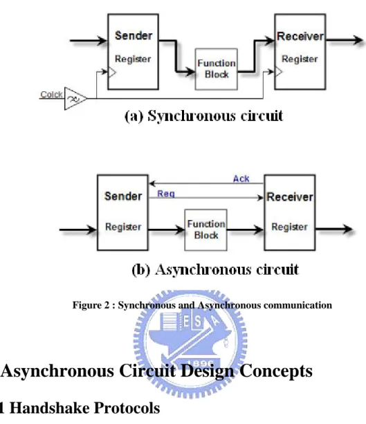
2.2 Synchronous vs. Asynchronous
The major difference between synchronous and asynchronous circuit design is the existence of global clock. In synchronous circuit, data transfer happens at specific time (clock rising and clock falling); in asynchronous circuit, latches transfer data by using handshake protocols. Handshake protocols are data transfer methods by adding two signals - Request and Acknowledge. “Request” is used to ask next stage to transfer data and “Acknowledge” is
Figure 2 : Synchronous and Asynchronous communication
2.3 Asynchronous Circuit Design Concepts
2.3.1 Handshake Protocols
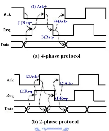
There are two major handshake protocols in asynchronous circuit design; they are 4-phase protocol and 2-phase protocol. The 4-phase handshake protocol is also called “Return-To-Zero (RTZ) signaling” or “Level signaling”. Similarly, the 2-phase handshake protocol is also called “Non-Return-To-Zero (NRZ) signaling” or “Transition signaling”. Generally, the 2-phase protocol seems to have better performance, but the implementation is more complex and chip area is getting larger caused by edge-triggered circuits. The Figure-3 is the signal diagram of two major handshake protocols, Figure-3(a) is the 4-phase protocol and Figure-3(b) is the 2-phase protocol.
Figure 3 : handshake protocol (a) 4-phase bundled-data (b) 2-phase bundled-data
2.3.2 Asynchronous encoding
There are several kinds of encoding for asynchronous circuit design, such as bundled-data (single-rail), dual-rail (1-of-2), 1-of-n (such as 1-of-4), and m-of-n.
The bundled-data refers to a situation where the data signals use normal Boolean levels to encode information, and where separate “Request” and “Acknowledge” wire are bundled with the data signals. To deserve to be mentioned, the “Request” signal must arrive to the receiver later than data. The Figure-4 is the bundled-data encoding.
Figure 4 : Bundled-data encoding
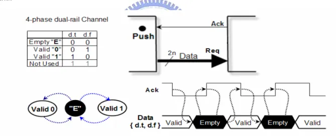
The dual-rail protocol encodes the “Request” signal into the data signals using two wires per bit of information that has to be communicated. Figure-5 is the diagram of 4-phase dual-rail, while the Figure-6 is the 2-phase dual-rail protocol diagram. Furthermore, the dual-rail protocol has an important feature that the “Request” signal embedded in the data.
Figure 5 : 4-phase dual-rail protocol
The 1-of-4 protocol is similar to the dual-rail protocol. It encodes each 2-bit with 4 wires. The encoding method is shown in Figure-7. It often puts in use of One-Hot DECODER / DEMUX ICs. The advantage of 1-of-4 encoding is for half-power consumption, because only half transition is needed when a new data comes.
2-bit data
1-of-4 encoding
00
1
000
01 0
1
00
10 00
1
0
11 000
1
Null 0000
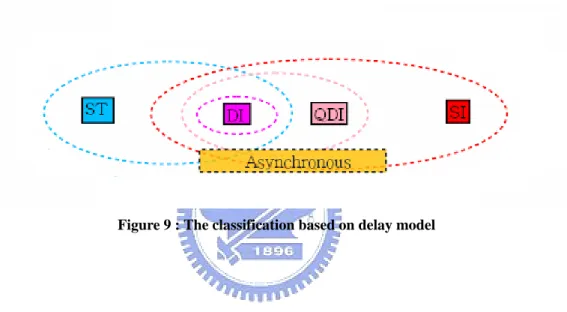
Figure 7 : 1-of-4 encoding2.3.3 Classification of asynchronous circuit
We now describe the classification of asynchronous circuit. In Figure-8, it is a circuit fragment with gate and wire delays. The dA, dB, and dC are gate delays, and the D1, D2, and
D3 are wire delays. The output of gate-A forks to the inputs of gate-B and gate-C. At this
gate level model, asynchronous circuits can be classified into Delay-Insensitive (DI), Quasi-Delay-Insensitive (QDI), Speed-Independent (SI), and Self-Timed (ST).
Figure 8 : A circuit fragment with gate delays and wire delays
1. Delay-Insensitive (DI), a circuit that operates correctly with positive, bounded but arbitrary delays in wire and gates. This means arbitrary dA, dB, dC, D1, D2, and D3
2. Quasi-Delay-Insensitive (QDI), is DI with the special case of some carefully identified wire forks call “Isochronic forks [4][5][6]”. This means arbitrary dA, dB, dC, D1
but D2 = D3. QDI is theoretically equivalent to SI .
3. Speed-Independent (SI), a circuit that operates correctly assuming positive, bounded but arbitrary delays in gates and ideal zero-delay wires. This means arbitrary dA, dB, dC but D1
= D2 = D3 = 0. But assuming ideal zero-delay wires is not very realistic in today’s
semiconductor processes.
4. Self-Timed (ST), speed-independence and delay-insensitivity introduced above are mathematically well defined properties under the unbounded gate and wire delay model. Circuits whose correct operation relies on more elaborate and/or engineering timing assumptions are simply called self-timed.
Table 1 : Classification of asynchronous circuit
Classification Gate Delay Wire Delay
DI Delay-Insensitive arbitrary arbitrary
QDI Quasi-DI arbitrary arbitrary D1, and D2 = D3
SI Speed-Independent arbitrary D1 = D2 = D3 = 0
ST Self-Timed Requires some timing assumptions
The following figure shows the scope of the classification based on delay model.
Chapter 3 Review of
FFT Algorithms
The Discrete Fourier Transform (DFT) plays an important role in many modern applications of Digital Signal Processing (DSP), such as linear filtering, correlation analysis and spectrum analysis [7]. The famous Fast Fourier Transform (FFT) algorithm was proposed by Cooley and Tukey in 1965 [8]. Through breaking the DFT into smaller DFTs, it provids a lot of ways to reduce the computational complexity from O( N2 ) to O(N‧
log2N).
3.1 The DFT algorithm
A Discrete Fourier Transform (DFT) is a transform that is defined as
Ν 1 N =0 -[ ] [ ] X n k n x n k =
∑
⋅W
⋅ k = 0, 1 … N-1 (3.1) where 2 N N W j e π ⎛ ⎞ − ⎜⎝ ⎟⎠ = (3.2) is the N-th root of unity.By Euler’s relationship: cos sin j e+θ = θ + j θ (3.3) cos sin j e−θ = θ − j θ (3.4) The term n kN
W
⋅ is DFT Coefficient, also called the Twiddle Factor. We will discuss itThe inverse of DFT (IDFT) is defined as Ν-1 -N =0 [ ] 1 [ ] N X n k n x n =
∑
k ⋅W
⋅ n = 0, 1 … N-1 (3.5)These equations show that the complexity of a direct computation of DFT/IDFT is O(N2); hence the long transforms will be very costly in a straight forward computation. The FFT algorithm deals with these complexity problems by exploiting regularities in the DFT algorithm.
3.2 The properties of twiddle factor
In formula (3.1), the main control parameter is
W
n kN⋅ . The DFT coefficient is also called the twiddle factor. The partial twiddle factor is shown as following.1. Periodic property: (360O) N N N N N ( 1) N k k k
W
+ =W W
⋅ = + ⋅W
(3.6) 2. Symmetry property: (180O) ( )N ( )N 2 2 N N N ( 1) N k k kW
W
W
W
+ = ⋅ = − ⋅ (3.7)3.3 The FFT algorithm
FFT algorithms are based on the fundamental principle of decomposing the computation of the DFT of a sequence of length N into successively smaller Discrete Fourier Transforms. The regularity of the FFT algorithm makes them running fan in VLSI implementation.
FFT algorithms follow the Divide-and-Conquer approach [9], are recursive in structure. By this approach, we can consider FFT with two parameters, n and k in Discrete Fourier Transform formula (3.1), and then form the two versions of FFT, DIT (Decimation-In-Time) and DIF (Decimation-In-Frequency). The Radix-2 algorithms are the simplest FFT algorithms. Let us take Radix-2 FFT for examples.
3.4 The Radix-2 DIT/DIF FFT
3.4.1 The Radix-2 FFT (DIT Version)
The Radix-2 Decimation-In-Time (DIT) FFT algorithm rearranges the DFT equation into two parts: a sum over the Even-numbered Discrete-Time indices for n = 0,2,4, … N-2 and a sum over the Odd-numbered indices for n = 1,3,5, … N-1. The outputs of these shorter FFTs are reused to compute many outputs, thus greatly reducing the total computational cost.
Recall the DFT formula (3.1) Ν-1 N =0 [ ] [ ] X n k n x n k =
∑
⋅W
⋅ k = 0, 1 … N-1Assume Even-numbered points with n = 2r, Odd-numbered points with n = 2r+1, the formula can be rewritten s following.
=Even N =Odd N [ ] [ ] [ ] X n k n n k n x n x n k =
∑
⋅W
⋅ +∑
⋅W
⋅ N N 1 1 2 2 2 (2 ) N N = =0 1 0 2 2 1 [ ] k [ ] k r r r r x rW
x rW
− − ⋅ + ⋅ + ⋅ ⋅ =∑
+∑
r = 0, 1 … (N/2)-1 N N 1 1 2 2 N N =0 2 2 =0 k N 2 2 1 [ ] kW
[ ] k r r r r x rW
x rW
− − ⋅ ⋅ ⋅ + ⋅ =∑
+ ⋅∑
(Substitution by N 2 N 2rk r kW
⋅ =W
⋅ ; Because N 2 2 2 N 2 2 N 2rk j N rk j rk rkW
e
e
W
π π ⎛ ⎞ ⎛ ⎞ − ⋅ ⋅ − ⎜ ⎟⋅ ⋅ ⎜ ⎟ ⋅ = ⎝ ⎠ = ⎝ ⎠ = ⋅ ) N N 1 1 2 2 N N 2 2 =0 N =0 2 2 1 [ ] r k [ ] r k r r k r xW
W
x rW
− − ⋅ ⋅ + ⋅ ⋅ =∑
+ ⋅∑
N [ ] k [ ] G kW
H k = + ⋅Thus we can get the first level decomposition of Radix-2 DIT FFT s following
formula. N [ ] [ ] [ ] X k k =G k +W ⋅H k k = 0, 1 … N-1 (3.8) where N1 2 N 2 =0 [2 ] [ ] r k r x r G k
W
− ⋅ ⋅ =∑
r = 0, 1 … (N/2)-1 (3.9) NWe take Radix-2 DIT FFT with N=8 for example, see the following 8-points Radix-2 DIT FFT diagram. Notice that, with Periodic Property (3.6)
G[4]=G[0], G[5]=G[1], G[6]=G[2], G[7]=G[3] and
H[4]=H[0], H[5]=H[1], H[6]=H[2], H[7]=H[3]
We can get the following Butterfly diagram:
Let us continue to decompose G[k] and H[k] in formula (3.6) and (3.7) using the same method. Recall N 1 2 N 2 =0 [2 ] [ ] r k r x r G k
W
− ⋅ ⋅ =∑
from formula (3.7). N N 1 1 4 4 N N 2 2 =0 = 2 (2 1 0 ) 2 1 [ ] [2 ] [ ] k k s s s s x s x s G kW
W
− − ⋅ + ⋅ ⋅ + ⋅ =∑
+∑
N N 1 1 4 4 N N N 4 4 4 = 2 =0 0 [ ]2 s kW
k [2 1] s k s s s xW
x sW
− − ⋅ ⋅ ⋅ + ⋅ =∑
+ ⋅∑
N 4 2 [ ]W
k [ ] g h G k G k = + ⋅ (3.11) Similarly, recall N 1 2 N 2 =0 [2 1] [ ] r k r x r H kW
− ⋅ + ⋅ =∑
from formula (3.8) N1 N1 4 4 N N 2 2 =0 = 2 (2 1 0 ) 2 1 [ ] [2 ] [ ] k k s s s s x s x s H kW
W
− − ⋅ + ⋅ ⋅ + ⋅ =∑
+∑
N N 1 1 4 4 N N N 4 4 4 =0 =0 2 [2 ] s kW
k [2 1] s k s s x sW
x sW
− − ⋅ ⋅ ⋅ + ⋅ =∑
+ ⋅∑
N 4 2 [ ]W
k [ ] g h H k H k = + ⋅ (3.12) Then we can decompose for the second time to the following diagram.In the same way, last decomposition for 8-points Radix-2 DIT FFT will be as following diagram.
Figure 13 : 8-points Radix-2 DIT FFT (N=8) with decomposed 3 times
Then we can use the basic Radix-2 DIT FFT Butterfly unit as following diagram. For
the reason of 2 N N j n k n k e
W
π ⎛ ⎞ − ⎜ ⎟⋅ ⋅ ⋅ = ⎝ ⎠ => ( ) 2 11 11 2 2 cos sin 1 j j e e jW
π π π π ⎛ ⎞ − ⎜ ⎟⋅ ⋅ ⋅ = ⎝ ⎠ = − = − = −Apply to the properties of twiddle factor in formula (3.6), (3.7), we can convert the following equations. (N = 8) 4 0 N N
W
=−W
,W
5N=−W
1N , 6 2 N NW
=−W
andW
7N=−W
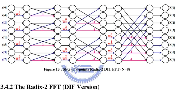
3N (3.13)Then we can use Radix-2 DIT FFT Butterfly unit and the equations in (3.13) to generate the following simplified SFG (Signal Flow Graphics) of 8-points Radix-2 DIT FFT.
Figure 15 : SFG of 8-points Radix-2 DIT FFT (N=8)
3.4.2 The Radix-2 FFT (DIF Version)
The Radix-2 Decimation-In-Frequency algorithm rearranges the DFT equation into two parts: computation of the Even-numbered Discrete-Frequency indices X[k] for k = 0,2,4 … N-2 (or X[2r]) and computation of the Odd-numbered indices for k = 1,3,5…N-1 (or X[2r+1]). This makes the Even points with k = 2r, and Odd points with k = 2r+1. Recursive application of this decomposition to the shorter-length DFTs results in the full Radix-2 DIF FFT.
Assume Even-numbered points with k = 2r, N-1 N =0 2 [ ] 2 [ ] X n n r x n r =
∑
⋅W
⋅ r = 0, 1 … (N/2)-1 N 1 N-1 2 N = 2 N N =0 2 2 [ ] rn [ ] rn n n x nW
x nW
− ⋅ ⋅ ⋅ ⋅ =∑
+∑
N N1 2 2 1 2 ( N) N 2 N N =0 =0 2 2 [ ] n [ ] r n n n r x nW
x nW
− − ⋅ ⋅ + ⋅ + ⋅ =∑
+∑
N1 N1 2 2 N 2 N N =0 2 0 2 = [ ] rn [ ] n rn n x nW
x nW
− − ⋅ ⋅ ⋅ + ⋅ =∑
+∑
(
)
N1 2 N N 2 2 =0 [ ] [ ] r n n x n x nW
− ⋅ + ⋅ + =∑
(3.14)So, we can get it by N
2
[ ] [ ]
x n +x n+ , then calculate the (N/2) points DFT.
Assume Odd-numbered points with k = 2r+1, N-1 N = (2 1) 0 [ ] 2 1 [ ] X n r n x n r+ =
∑
⋅W
⋅ + r = 0, 1 … (N/2)-1 N 1 N-1 2 N = 2 (2 1) (2 N N = 1) 0 [ ] r n [ ] r n n n x nW
x nW
− + ⋅ + ⋅ ⋅ ⋅ =∑
+∑
N1 N1 2 2 N 2 ( ) N 2 N N =0 =0 (2 1) (2 1) [ ] r n [ ] r n n n x nW
x nW
− − ⋅ ⋅ + + + ⋅ + ⋅ =∑
+∑
N 2 N1 N1 2 2 N 2 N N =0 =0 (2 1) (2 1) ( ) (2 1) N [ ] n [ ] n n n r r r x nW
W
x nW
− − ⋅ + + ⋅ + ⋅ ⋅ + ⋅ =∑
+ ⋅∑
N1 N1 2 (2 1) 2 N 2 N N =0 =0 (2 1) [ ] r n ( 1) [ ] n n r n x nW
x nW
− − ⋅ ⋅ + + ⋅ + ⋅ =∑
+ − ⋅∑
(
)
N1 2 (2 N 0 1) N 2 = [ ] [ ] n n r x n x nW
− + ⋅ − + ⋅ =∑
(
)
N 1 2 2 N N 2 N =0 [ ] [ ] rn n n x n x nW
W
− + ⋅ − =∑
⋅(
)
N 1 2 N N 2 2 N =0 [ ] [ ] r n n n x n x nW
W
− ⋅ − + ⋅ =∑
⋅ (3.15)So, we can get it by N
2
[ ] [ ]
x n −x n+ multiply with twiddle factor
N n
W
, then calculate the(N/2) points DFT. Then we show the diagram of 8-points Radix-2 DIF FFT.
Figure 16 : 8-points Radix-2 DIF FFT (N=8)
After decompose three times (that is N/R), such as derivation of DIT, we show the simplified SFG of 8-points Radix-2 DIF FFT
Then we can use the basic Radix-2 DIF FFT Butterfly unit as following diagram.
Figure 18 : Basic Radix-2 DIF FFT Butterfly unit
3.5 Other FFT algorithms
There are many other FFT algorithms, such as Fixed-Radix (Radix-4 [10][11][12], Radix-8 [13], Radix-16 [14], Radix-6 [15]), Radix-22 [16], Radix-23, Mixed-Radix (Radix-2/4 [17], Radix-2/8, Radix-2/4/8) …etc. We don’t deeply discuss them here. In preceding section, we described the basic derivation process of FFT by DIT and DIF. This is very important concept for the design of FFT processor. Afterward we will integrate the concepts with hardware circuit design.
Chapter 4 FFT Processor Architecture
In previous chapter, we introduced the FFT algorithm by DIT and DIF versions, and produced some examples by Radix-2 FFT. In this chapter, we will guide the theory of FFT algorithm to the physical design of FFT processor architecture.
4.1 FFT Processor Architecture
From W Li, L Wanhammar, “A pipeline FFT processor” [18], FFT processors can be divided into three main classes:
(1) Fully parallel FFT processors, the operations in the Signal Flow Graph are mapped isomorphically to a hardware structure. The implementations are hardware intensive but not practical for large FFTs.
(2) Column FFT processors, each stage in the FFT is computed with a set of processing elements and the resultant is fed back to the same processing element for the computation of the next stage.
(3) Pipelined FFT processors, they utilize concurrent processing of different stages to achieve high throughput. This is also called row-major or row-wise in some literatures. This is praised for the architecture of “Pipeline”.
4.2 Column FFT Processor
Column major FFT processor is efficient for distributed memory system [19]. See the following Figure-19. Permutation Network (PN) is responsible for stride permutation and
Figure 19 : Column major FFT architecture (DIT)
4.3 Pipelined FFT Processors
Similarly, the raw major FFT processor architecture is shown as following Figure-20. It needs only log NR Processing Elements (when N becomes more and more large, it
saves more PEs), but throughput time is N/R for each stage. There are three mainly pipelined techniques to improve the throughput; they are MDC (Multi-path Delay Commutator), SDC (Single-path Delay Commutator) and SDF (Single-path Delay Feedback) structures. We will introduce the MDC, SDF pipelined FFT structures later.
4.3.1 MDC (Multi-path Delay Commutator)
Multi-path Delay Commutator architecture includes three main components: Butterfly unit, Commutator (switch unit), and Register. The 8-points Radix-2 MDC structure can be shown as following diagram.
Figure 21 : 8-points Radix-2 DIF FFT Processor with MDC structure
This R2MDC is the most straightforward way to recognize that the data stream feeds into the FFT/IFFT with half at each stage. To be delayed through the register, memory or FIFO, and processed with the second half data stream. The delay for each stage is N/2, N/4, N/8… 2, and 1 respectively. The FFT processor of general R2MDC structure with N-points is shown as following diagram. It needs hardware cost with 3N-2
2 memory units, 2log N adders and 2
(
2)
4.3.2 SDF (Single-path Delay Feedback)
Single-path Delay Feedback is another interest structure of row major FFT processor. It also includes three main components: Butterfly unit, Twiddle Factor Multiplier and Register. The 8-points Radix-2 SDF structure is shown as following Figure-23.
Figure 23 : 8-points Radix-2 DIF FFT Processor with SDF structure
The first half input data stream passes unchanged into the register set (with length N/2) until it is full. At this moment, the incoming data and the data in the register are fed into the Butterfly unit that is computed with 2-point DFT. The output of first stage then sent to the rotational module. The rotator can be CORDIC [20][21] or complex multiply which applies the twiddle factors while the sequence is (N/2)+1 ~ N-1. When all N/2 pairs have been computed, the (N/2)+1 ~ N-1 are allowed to pass out of the register, and the next transform is being loaded into the register set. The entire computation is completed after log N 2 stages. The FFT processor of general R2SDF with N-points is shown as following diagram. It needs hardware cost with only N-1 memory units, 2log N adders and 2 2 log N 1
(
2 −)
Figure 24 : General R2SDF structure
The following table is the comparison of MDC and SDF FFT processors. We can see that the SDF structure needs smaller chip area and power consumption.
Table 2 : Comparison of MDC and SDF
Speed Scalable Modularity Area
Power Consumption
Complexity
MDC High High High Large High Simple
SDF High High High Small Low Medium
4.4 Comparison of Pipelined FFT Processors
The comparison of the pipelined FFT processors [22] is shown in the following Table 3. After analyzing and observing, the delay feedback structures are always more efficient than corresponding delay commutator structures in terms of memory utilization (response to chip area cost), since the stored Butterfly output can be directly used by the multipliers. Radix-2 based architectures have simpler Butterfly units which are better utilized.
Table 3 : Comparison of Pipelined FFT Processors
Structure FIFO Size Add/Sub Multiplier Control Circuit
R2MDC 3N/2 - 2 2 log2N 2 (log2N – 1) Simple
R4MDC 5N/2 - 4 8 log4N 3 (log4N - 1) Medium
R22MDC 3N/2 - 2 2 log2N 2 (log2N – 1) Simple
R2SDF N - 1 2 log2N 2 (log2N – 1) Simple
R4SDF N - 1 8 log4N 3 (log4N - 1) Medium
R22SDF N - 1 4 log4N 2 (log2N – 1) Simple
Chapter 5 Design and Implementation
In this chapter, we first illustrate the famous asynchronous components, such as C-element, Muller pipeline and various asynchronous pipelines ... etc., and then present the design of asynchronous FFT processor.
5.1 C-element
The Muller C-element, also called Muller C-gate, is a common asynchronous logic component proposed by David E. Muller in 1959 [23]. The result of C-element reflects the input when the states of all inputs match. The output then holds this state until the all inputs translate to the other state. The truth table of C-element is shown as following Table 4.
Table 4 : Truth table of C-element
C-element Input Output a b Z 0 0 0 0 1 unchanged 1 0 unchanged 1 1 1
The C-element symbol, gate-level implementation and wave form are shown as following. We can see that output Z only changes when input a and b are equal.
In transistor level, we illustrate the implementations in dynamic CMOS and Static CMOS.
Figure 26 : C-element with dynamic CMOS
In dynamic CMOS implementation, the weak inverter is for the intension of feedback easily, and the normal inverter is larger to reach the purpose of pushing next circuit. Dynamic logic is faster than static CMOS. For complex functions, the transistor count is almost halved. Therefore, dynamic logic consumes more power than static CMOS despite the lower transistor count.
Let us see the static CMOS C-element implementation. This type of logic guarantees the input to be VALID or LOW and thus allows arbitrary cascading. Even though static CMOS C-element has more area, and not faster as dynamic one, but it has excellences of stable and low static power consumption.
5.2 Asynchronous pipeline
5.2.1 coarse-grain and fine-grain pipeline
A pipeline is to break up a complex operation on a stream of data into simpler sequential operations. The coarse-grain pipeline is like to execute as a simple processor level. The fine-grain pipeline is like to work as pipelined adder. The purpose of pipeline is to increase the throughput.
5.2.2 Muller pipeline
The Muller pipeline [23], also called the Muller distributor, is built from C-elements and inverters, so it is Delay-Insensitive handshake machine. It applies on many asynchronous circuits.
Figure 29 : The Muller pipeline
In Figure-29, after all of the C-elements have been initialized to zero, the left
environment may start handshaking. Considering the
i
-th C-element C[i
], it will propagate a 1 from its previous stage C[i
-1], only if its next stage, C[i
+1], is 0. Similarly, it willpropagate a 0 from its previous stage C[
i
-1], only if its next stage, C[i
+1], is 1. Thinking of 1010101 as waves: 1010101 , the C-elements propagate waves precisely.
5.2.3 4-phase bundled-data pipeline
4-phase bundled-data is the most closely resembles the design of synchronous circuits and which normally leads to the most efficient circuits, due to the extensive use of timing
Figure 30 : 4-phase bundled-data pipeline
A 4-phase bundled-data pipeline is particularly simple. A Muller pipeline is used to generate local clock pulses. The clock pulse generated in one stage overlaps with the pulses generated in the neighboring stages in a carefully controlled interlocked manner. To
maintain correct behavior matching delays have to be inserted in the request signal paths. This pipeline implementation is particularly simple but it has some disadvantage, such as speed and throughput, if a pipeline or FIFO depends on the time, it must take to complete a handshake cycle.
5.2.4 2-phase bundled-data pipeline (Micropipelines)
A 2-phase bundled-data pipeline was proposed by Ivan E. Sutherland in his famous Turing Award “Micropipelines” lecture in 1989 [24]. It uses a Muller pipeline as the main control circuit. The control signals are also defined as events or transitions.
Figure 31 : 2-phase bundled-data pipeline (Micropipelines)
A kind of special Capture-Pass latches are needed, see the right side of Figure-31, events on the Capture and Pass inputs alternate, causing the latch to alternate between capture mode and pass mode. This 2-phase bundled-data approach is elegant and efficient, compared to the 4-phase bundled-data approach. However, the implementation of
5.2.5 4-phase dual-rail pipeline
The 4-phase dual-rail pipeline is another Muller pipeline with Completion Detection. The following Figure-32 is a 1-bit wide and three stage deep pipeline. It can be thought of two Muller pipeline connected in parallel, using a common acknowledge signal per stage to synchronize operation. The pair of C-elements in a pipeline stage can store the EMPTY codeword {d.t, d.f} = {0, 0}, causing the acknowledge signal out of that stage to be 0, or it can store one of the two VALID codeword {0, 1} and {1, 0}, causing the acknowledge signal out of that stage to be logic 1. Because the codeword {1, 1} is Not-Used, the
acknowledge signal generated by the OR gate safely indicates the state of the pipeline stage as being VALID or EMPTY. This type of pipeline is the essence of QDI circuit.
Figure 32 : 4-phase dual-rail pipeline
5.3 8-points Radix-2 DIF FFT with SDF structure
5.3.1 Data flow
Recall the 8-points Radix-2 DIF FFT with SDF structure. We analyze the data flow step by step. In the following diagram, step (a) is the initial state,
And step (b) (c) (d) (e) are the first 4 steps of input data x[0], x[1], x[2], x[3]. They will feed into the FIFO or Shift-Registers.
In step (f), FIFO pops out x[0] and combines with next input x[4] to calculate by Butterfly unit. Afterwards, the subtraction of x[0] and x[4] feedback to the FIFO, and addition of x[0] and x[4] passes through to next stage.
In step (i), the data in FIFO passes through to next stage only. The rest parts are deduced by the same analogy.
Figure 33 : Data flow of 8-points Radix-2 DIF FFT with SDF structure
From the analysis of data flow above, we can understand the concept of pipeline stages. In the later section, we use the 4-phase dual-rail pipeline control circuit to implement the FFT processor.
5.3.2 Butterfly units
From the above section, we observe that the Butterfly units work with two operation modes.
Figure 34 : Two operation modes of R2SDF Butterfly units
In the left diagram (a), it just pushes the input data into the FIFO and pops the data from the FIFO to the output. In the right diagram (b), it pops the addition part to the next stage and feeds back the subtraction part to the FIFO. Obviously, it follows a regular pattern.
5.4 Implementation of 4-phase dual-rail asynchronous
circuit
In this section, we provide the implementation of 4-phase dual-rail asynchronous circuit. After constructing the basic component devices, we can build up the full architecture of FFT processor by these basic components. It will benefit to flexibility, scalability and for the purpose of reuse for designing other circuits.
5.4.1 4-phase dual-rail AND gate
Figure 35 : 4-phase dual-rail AND gate
The 4-phase dual-rail AND gate implements by four C-element and one OR gate. The output Z is True only if input x and y are all True. When input x{0,0} and y{0,0} are all EMPTY, the output Z is also EMPTY. In other status, the Z keeps its value.
5.4.2 4-phase dual-rail OR gate
5.4.3 4-phase dual-rail JOIN, FORK
The 4-phase dual-rail JOIN does not involve any components, as the request signal is encoded into the data. But acknowledge from this stage must b forked to all of the previous stages to notice them that this stage is ready.
Figure 37 : 4-phase dual-rail JOIN
The 4-phase dual-rail Fork involves a C-element to combine the acknowledge signals on the output channels into a signal acknowledge signal on the input channel. From a control point of view, a JOIN synchronizes several input channels and a Fork synchronizes several output channels.
5.4.4 4-phase dual-rail MERGE
To analysis the 4-phase dual-rail MERGE, we show the truth table as following diagram. When input “b” and “c” is EMPTY, the output “a” is also EMPTY. Therefore, when input “b” or “c” transfer data (only “b” or “c” one input at the same time), the output “a” transfer to the sate of “b” or “c”. The other status, the output “a” keeps its status.
Table 5 : Truth table of 4-phase dual-rail MERGE
Then we implement the circuit by the following diagram, and its wave form after simulation is presented.
Figure 39 : 4-phase dual-rail MERGE circuit
The 16-bits 4-phase dual-rail MERGE is implemented in the Figure-40.
5.4.5 Completion Detection
In the above MERGE circuit, we use the Completion Detection circuit to acknowledge previous stage. An N-bit wide pipeline can be implemented by using a number of 1-bit pipelines in parallel. This does not guarantee to a receiver that all bits in a word arrive at the same time, but often the necessary synchronization is done in the function blocks. On the other hand, for the purpose of solving fan-in problem, we implemented the Completion Detection circuit as following diagram.
When all inputs become EMPTY the C-element is set low, and the output is low. As usual, it can acknowledge previous stage to calculate and transfer data. When input data with VALID status, by the characteristic of dual-rail, the “All Valid” point will be set high, then the output is high. By acknowledge, it will prevent the previous stage to transfer data.
5.4.6 4-phase dual-rail Full Adder / Subtracter
To implement the 4-phase dual-rail full adder, see the following truth table first.
Table 6 : Full Adder Truth Table
Then we implement PLA-like structure of the circuit to illustrates DIMS (Delay Insensitive Minterm Synthesis) – because the circuits are Delay-Insensitive and the C-elements in the circuits generate all minterms of the input variables.
Then we can use the Adder to implement the Subtracter by following circuit.
Figure 43 : 4-phase dual-rail Subtracter
5.4.7 4-phase dual-rail DEMUX / MUX
4-phase dual-rail DEMUX perform the function of steering the input to one of the several outputs. The control input is a channel just like the data inputs and outputs. A DEMUX will synchronize the control and data input channels and steer the input to the selected output channel. The following diagrams are the truth table (Table-7), implemented circuit and simulation wave form (Figure-44).
Table 7 : 4-phase dual-rail DEMUX
x sel Y_f Y_t Z_f Z_t
Empty Empty 0 0 0 0 No change F F 1 0 No change F T No change 1 0 T F 0 1 No change T T No change 0 1
After implementation of DEMUX, it is easy to implement MUX. A MUX will synchronize the control channel and the relevant input channel and send the input data to the output.
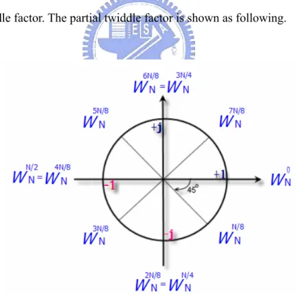
5.5 Implementation of Twiddle Factor
Let’s see the 8-points FFT Twiddle Factor. The 4-phase dual-rail Radix-2 DIF SDF FFT processor applies the approximation approach [25] to solve the problem, and it saves the Multiplier circuit.
Figure 46 : 8-points FFT Twiddle Factor
From the following formula in approximation approach:
, (5.1)
2 / 2
1 3 4 6 8 14
− − − − − −
We can use the shift register to get the by the following circuit.
Figure 47 : The method to solve sqrt(2) / 2
5.6 Radix-2 DIF SDF FFT Stage Schematic
After analysis of data flow, Butterfly unit, 4-phase dual-rail implementation circuit and solved issue of twiddle factor, the proposed stage architecture is shown in Figure-48. The data width of the design is 16-bits width complex numbers, combined with x[n]r_t, x[n]r_f (real numbers) and x[n]i_t, x[n]i_f (imaginary numbers).
In Figure-48, the initial states of all components are set to MMPTY by C-element reset mechanism. Through the DEMUX, the first four inputs x[n] pass to the FIFO, and trigger the control counter to add one. When the FIFO is full, it pops x[i] and calculates with x[i+4], and then goes to the Butterfly unit (Adder / Subtracter or pass through circuit). The
subtraction will feedback to FIFO, and the addition part goes through to the twiddle factor unit. Then it pushes to the next stage. The data is controlled by 4-phase dual-rail pipeline circuit.
5.7 The Simulation Result
In order to verify the correctness of the design, ALTERA QuartusII 9.0sp1 and ModelSim6.4a are used. Figure-49 shows the waveform of the functional simulation. We also tried to synthesize gate-level design with Synopsys Design Compiler with TSMC 0.13 µm CMOS process technology. The result is correct, too.
Figure 49 : The wave from of Simulation Result
5.8 The Area Report
The area of related elements is shown in the following Table-8.
Table 8 : The area report of related elements
element area(µm2) C_element 25.460982 CD16 629.825317 DEMUX16A2 3842.230327 AsyncFIFO16_v06 43249.340919 ADDER16A1 28823.926428 SUB16A1 30182.340892
Table 9 : The area report of proposed FFT processor
Process Area(µm2)
_SyncFFT TSMC 0.13 µm 290938.327653
_AsyncFFT (bundle-data) TSMC 0.13 µm 337901.802623
_AsyncFFT (proposed) TSMC 0.13 µm 423705.245301
The proposed asynchronous FFT consists of a lot of C-elements and is larger than synchronous one. But it is noticed that the area of twiddle factor is reduced by shift register in proposed asynchronous FFT. It is different from the multiplier in synchronous FFT.
5.9 The Power Consumption Report
Power consumption is estimated by PowerPlay Power Analyzer. It’s also used the TSMC 0.13 µm CMOS process technology. The voltage is set to 1.5V identically. The dynamic power consumption of synchronous FFT is about 58 mw with operating speed of 50 MHz. Relatively, the dynamic power consumption of asynchronous FFT is about 54 mw. Clearly, it saves about 6.8966% power. We can analogize that when the points of FFT processor increase, it will save more power.
Table 10 : The power consumption report
FFT version Process Dynamic Power(mw)
_SyncFFT TSMC 0.13 µm 58 mw
_AsyncFFT (bundle-data) TSMC 0.13 µm 57 mw
Chapter 6 Conclusions and Future Works
In this thesis, we proposed the design of an Asynchronous FFT processor, 8-points 4-phase dual-rail Radix-2 DIF SDF FFT processor. This design method removes the global clock, avoids the clock skew, and is tolerant to variations in supply voltage, temperature and fabrication process parameters.We simulated with ALTERA FPGA devices (such as Lowest Power / Highest
Performance Stratix Series, and Low-Cost Cyclone Series). We also simulated the synthesis with TSMC 0.13 µm process by Synopsys Design Compiler. We used ModelSim to make sure that it works correctly. Although the area is larger than synchronous one (about 1.45 times), but it saves about 6.90% power.
The benefit of asynchronous dual-rail circuits is that it automatically acknowledges to previous circuit. It doesn’t need to fine tune the delay-match in bundled-data. But the cost is still too high. We may use mix mode to reduce the area cost.
In the future work, if we want to design more points of asynchronous FFT processors, the ROM-based or Look up table (LUT) mechanisms are needed. It will become more complex. Additional address mode circuits should also be designed. It may be suitable for ASIC architecture. That may be worth to investigate.
References
[1] Brigham O.E., The Fast Fourier Transform and its Applications, Prentice Hall, 1988, pp. 23-28.
[2] J. Melander, T. Widhe, L. Wanhammar, “An FFT processor based on the SIC architecture with asynchronous PE,” IEEE 39th Midwest symposium, Circuits and Systems Vol.3, 1996, pp. 1313-1316.
[3] R. Seshasayanan, S.K. Srivatsa, V. Sugavaneswaran, “Implementation of an Asynchronous FFT ,” INDICON 2005 Program, 2005 Annual IEEE, Dec. 2005,
pp.327-331.
[4] C.H. van Berkel. “Beware the isochronic fork, ” SOURCE, INTEGRATION, the VLSI journal, Vol.13, Issue 2, June. 1992, pp. 103-128.
[5] C.H. van Berkel, F. Huberts, and A. Peeters, Stretching quasi delay insensitivity by means of extended isochronic forks. In Asynchronous Design Methodologies, IEEE Computer Society Press, May 1995, pp. 99-106.
[6] Chang-Jiu Chen, Wei-Min Cheng, Hung-Yue Tsai, Jen-Chieh Wu, “A Quasi-Delay-Insensitive Microprocessor Core Implementation for Microcontrollers,” Journal of Information Science and Engineering, Vol.25, Issue 2, March 2009, pp. 543-557. [7] E. Chu and A. George, Inside the FFT Black Box : Serial & Parallel Fast Fourier Transform Algorithms, CRC Press LLC, 2000, pp. 336.
[8] J. W. Cooley and J. W. Tukey, “An Algorithm for Machine Computation of Complex Fourier Series,” Math. Computation, Vol.19, 1965, pp. 297-301.
[9] Thomas H. Cormen, Charles E. Leiserson, Ronald L. Rivest and Clifford Stein, Introduction to Algorithms, MIT Press, 1990, pp. 822-848.
[10] Zhijian Sun, Xuemei Liu, Zhongxing Ji, “The Design of Radix-4 FFT by FPGA,” Proceedings of the 2008 International Symposium on Intelligent Information Technology Application Workshops, Dec. 2008, pp.765-768.
[11] VFJ Alberto, RTR de Jesus, OM Alejandro, “VHDL core for 1024-point radix-4 FFT computation,” IEEE Reconfigurable Computing and FPGAs, ReConFig 2005
International Conference, Sep. 2005, pp. 23-24.
[12] K Nadehara, T Miyazaki, I Kuroda, “Radix-4 FFT implementation using SIMD multimedia instructions,” IEEE International Conference on Acoustics, Speech, Vol.4, 15-19 March 1999, pp. 2131-2134.
[13] S Bouguezel, MO Ahmad, MNS Swamy, “Improved radix-4 and radix-8 FFT algorithms,” IEEE Transactions on Digital Object Identifier Vol.3,May 2004, pp. 561–564. [14] Takahashi, D., “A radix-16 FFT algorithm suitable for multiply-add instruction based on Goedecker method", ICME '03. Proceedings, Multimedia and Expo, 2003, pp. 665-668.
[15] S. Prakash, V. Rao, “A new radix-6 FFT algorithm,” IEEE Transactions on Acoustics, Speech and Signal Processing Vol. 29, Issue 4, Aug. 1981, pp. 939-941. [16] Cho, MS Kim, DB Kim, JU Kim, “R22SDF FFT Implementation with Coefficient Memory Reduction Scheme,” IEEE 64th 25-28, Vehicular Technology Conference, 2006, pp. 1-4.
[17] Moon, Y Kim, “A mixed-radix 4-2 butterfly with simple bit reversing for ordering the output sequences ,” ICACT, Advanced Communication Technology, 2006, pp.1773-1774.
[19] N. Anupindi, M. An, James W. Cooley, Q. Yang, “A New and Efficient FFT Algorithm for Distributed Memory Systems, ”Proceedings of the 1994 International Conference on Parallel and Distributed Systems, 19-21 Dec. 1994, pp. 107-112. [20] SY Park, NI Cho, SU Lee, K Kim, J Oh, “Design of 2K/4K/8K-point FFT processor based on CORDIC algorithm in OFDM receiver,” IEEE Pacific Rim Conference on Communications, Computers and signal Processing, PACRIM, Vol.2 , Aug. 2001, pp. 457-460.
[21] E. Grass, B. Sarker and K. Maharatna, “A Dual Mode Synchronous / Asynchronous CORDIC Processor,” IEEE International Symposium, Proc.8th on Asynchronous Circuits and Systems, Manchester, U. K., April 2002. pp. 76-83.
[22] S. He, M. Torkelson, “A New Approach to Pipeline FFT Processor,” Parallel Processing Symposium, 1996, pp.766-770.
[23] D. Muller and W. Bartky, “A theory of asynchronous circuits,” in Proceedings of International Symposium on the Theory of Switching, 1959, pp. 204-243.
[24] Ivan E. Sutherland, “Micropipelines,” Turing Award Lecture, Communications of the ACM, Vol. 32, 1989, pp. 720-738.
[25] L. Jia, Y. Gao, J. Isoaho and H. Tenhunen, “A New VLSI-Oriented FFT Algorithm and Implementation,” IEEE ASIC Conference in Proceedings, 1998, pp. 337-341.