國 立 交 通 大 學
電子工程學系 電子研究所碩士班
碩 士 論 文
非均質矽鍺奈米線在高靈敏度生物感測器之新穎應用
Novel Application of Non-homogeneous SiGe Nanowire
for Highly Sensitive Biosensor
研 究 生 : 滕 聚 翔
指導教授 : 張 國 明 博士
Novel Application of Non-homogeneous SiGe Nanowire for
Highly Sensitive Biosensor
研 究 生:滕聚翔 Student:Chu-Hsiang Teng
指導教授:張國明 博士 Advisor:Dr. Kow-Ming Chang
國 立 交 通 大 學
電子工程學系 電子研究所碩士班
碩 士 論 文
A Thesis
Submitted to Institute of Electronics
College of Electrical Engineering and Computer Science
National Chiao Tung University
In Partial Fulfillment of the Requirements
for the Degree of
Master
In
Electronics Engineering
September 2008, Hsinchu, Taiwan, Republic of China
中華民國九十七年九月
非均質矽鍺奈米線在高靈敏度生物感測器之新穎應用
研究生:滕聚翔
指導教授:張國明 博士
國立交通大學
電子工程學系 電子研究所碩士班
摘
要
矽奈米線在近年來被廣泛研究,尤其在感測元件的應用上被視為最具
潛力的材料之一。本實驗室團隊也成功製做出矽鍺奈米線,並證實矽鍺奈
米線同樣具有感測功能,可作為生物感測器之用。在本論文研究中,我們
利用半導體製程技術製作 n 型與 p 型的矽鍺奈米線與矽奈米線,並比較矽
鍺奈米線與矽奈米線元件的感測特性,探討矽鍺奈米線與矽奈米線感測元
件之差異。由矽鍺奈米線與矽奈米線比較之結果,我們更進一步提出非均
質結構之矽鍺奈米線,利用矽鍺氧化時的鍺析出現象,我們成功製作出非
均質結構,並探討此製程技術最重要的溫度因素,最後證實非均質矽鍺奈
米線比均質化的奈米線有更高的感測能力。
Novel Application of Non-homogeneous SiGe Nanowire for
Highly Sensitive Biosensor
Student:Chu-Hsiang Teng
Advisor:Kow-Ming Chang
Department of Electronics Engineering & Institute of Electronics
National Chiao Tung University
ABSTRACT
Si nanowire has attracted a lot of attention and been studied to a great extent. It is considered as one of the most promising candidate for chemical or biological sensing application. In our previous study, we successfully demonstrated the sensing capability of SiGe nanowire-based bio-sensor. In this thesis, p-type and n-type SiGe and Si nanowires were fabricated by sidewall spacer formation, which is compatible to VLSI technology. The changes of electrical characteristics of nanowires corresponding to APTMS and BS3 modification were studied. Then we proposed a non-homogeneous structure to improve sensing capability. Non-homogenous SiGe nanowires were fabricated by Ge condensation
technique. Thermal process was investigated and discussed. In this study, 900℃ annealing for 30 minutes after oxidation led to highest conductance change and sensitivity. Also, we proved that non-homogeneous SiGe nanowire exhibited higher response than homogeneous SiGe nanowire.
誌 謝
首先要感謝張國明老師在這兩年中的指導,讓我在學業上能有所精
進,除了學術上的指導,老師也時常與我們分享人生的經驗與待人處事的
道理,不管是生活上或學術上都對我有莫大的幫助。
其次要感謝實驗室的學長同學學弟們,尤其是郭俊銘學長、梁家榮學
長、趙文全學長、鄭文魁學弟、以及王育彬學弟,感謝大家對我在專業知
識上的指導與實驗上的協助。另外特別感謝同屆的幾位同學們,因為有大
家互相的鼓勵與幫忙,我才得以完成這篇論文。
此外要感謝羅正忠老師與羅老師實驗室的陳永裕、謝智仁兩位學長在
實驗上的幫助,更感謝交大與 NDL 提供這麼好的研究環境與資源,讓我能
在這麼好的環境精進我的學問。
最後要感謝的是我的家人們,家人在我背後的支持是讓我能順利碩士
畢業的最大力量。
誌于 2008. 09
滕聚翔
Contents
Abstract (Chinese) ...i
Abstract (English)...ii
Acknowledgement...iv
Contents... v
Figure Captions...viii
Chapter 1. Introduction ... 1
1.1 Overview of nanowire sensors ...1
1.2 Silicon nanowire sensor...2
1.2.1 Silicon nanowire fabrication...2
1.2.1.1 Bottom-up approaches of SiNW fabrication ...2
1.2.1.2 Top-down approaches of SiNW fabrication ...4
1.2.2 Applications of SiNW sensors...6
1.2.2.1 pH detection...6
1.2.2.2 Protein detection...7
1.2.2.3 DNA detection ...8
1.2.2.4 Virus detection...8
1.3 Other nanowire sensors ...9
1.3.1 Metal oxide nanowire sensor...9
1.3.3 Conducting polymer nanowire sensor ...12
1.3.4 Carbon nanotube sensor ...14
1.4 SiGe nanowire IgG sensor...15
1.5 Sensitivity ...15
1.6 Motivation ...17
1.7 Ge condensation technology...18
1.7.1 Oxidation behavior of SiGe...19
1.7.2 Oxidation mechanism of SiGe...20
1.8 Thesis organization...21
Chapter 2. Experiment... 23
2.1 Process flow...23
2.2 Functionalization ...24
2.3 Measurement of electric characteristics ...25
Chapter 3.SiGe and Si Nanowire Sensors ... 26
3.1 Cross-section view of poly-crystalline SiGe and Si nanowires...26
3.2 Electrical characteristics of SiGe and Si nanowire sensors before and after APTMS and BS3 modification...26
3.3 Sensitivity of Si0.8Ge0.2 and Si nanowire sensors to APTMS ...29
3.4 Conductance change and sensitivity of blank nanowires to DI water and BS3 ...30
4.1 Achieving non-homogeniety by dry oxidation at 900℃ for 4 minutes...31
4.2 Electrical characteristics of Si0.93Ge0.07 nanowires after oxidation ...31
4.3 Effect of annealing on conductance change ...32
4.4 Effect of annealing on conductance of nanowires...34
4.5 Annealing at 900℃ for 30 minutes after ion implantation...34
4.6 Estimation of surface charge density…..……… 35
4.7 Effect of annealing on poly-Si nanowires ...36
Chapter 5. Conclusion ... 37
Chapter 6. Future work ... 39
Figure Captions
Fig. 1-1. Numerical simulation result of the relationship between the response time (ts) and the detectable concentration (ρ0) of a DNA sensor[1]. ...40 Fig. 1-2. Images of sample and setup, with (a) showing the chip layout with gold pads and
(b)showing the central device area. The positions of the nanowires are indicated by letters A C. In (c) a schematic cross-section of the etching setup with a mounted sample is shown, and in (d) a schematic cross-section of the nanowire during
etching is shown [14]...40 Fig. 1-3. (A) schematic after anisotropic etch. The silicon-on-insulator active channel (yellow,
width w and thickness t) is undercut etched, whereas degenerate leads (red) are etch-resistant. (B) SEM image of a device[15]. ...41 Fig. 1-4. (A) Schematic illustrating the conversion of a NWFET into NW pH sensor. (B)
Real-time response of an APTES-modified SiNW for pHs from 2 to 9. (C) Plot of the conductance versus pH. (D) The conductance of unmodified SiNW versus pH[20]...41 Fig. 1-5. (A) A biotion-modified SiNW and subsequent binding of streptavidin to the SiNW
surface. (B) Plot of conductance versus time for a biotin-modified SiNW,where region 1 correspond to buffer solution,region 2 corresponds to the addition of
250nM streptavidin[20]. ...42 Fig. 1-6. Optical image (top) of a nanowire device array. The schematic illustration (bottom)
electrodes connecting nanowires, which is blue lines here[21]...42 Fig. 1-7. Complementary sensing of PSAusing p-type (NW1) and n-type (NW2)
silicon-nanowire devices in the same array[21]. ...43 Fig. 1-8. Conductance-versus-time data recorded for the simultaneous detection of PSA,
CEA and mucin-1 on p-type silicon-nanowire array in which NW1, NW2 and NW3 were functional-ized with mAbs for PSA, CEA and mucin-1, respectively. The solutions were delivered to the nanowire array sequentially as follows: 1) 0.9 ng/mL PSA, 2) 1.4 pg/mL PSA, 3) 0.2 ng/mL CEA, 4) 2 pg/mL CEA, 5) 0.5 ng/mL
mucin-1, 6) 5 pg/mL mucin-1[21]. ...43 Fig. 1-9. Modification scheme of the SiNW surface for the DNA detector: (1) self-assembly
of 3-mercaptopropyltrimethoxysilane (MPTMS); (2) covalent immobilization of DNA probes; (3) DNA detection based on hybridization between label-free complementary DNA target and the immobilized DNA probes on the SiNW
surfaces. The inset is the SPV signal on a p-type Si surface at different stages of the modification[76]. ...44 Fig. 1-10. Conductance of the same p-type SiNW, where the arrow indicates the addition of
25pM complementary DNA (GGA TTA TTG TTA) solution[76]. ...44 Fig. 1-11. Conductance (Upper) and optical (Lower) data recorded simultaneously vs. time for a single silicon nanowire device after introduction of influenza A solution[23]. ....45 Fig. 1-12. SEM (A), TEM (B), z-axis amplified AFM micrographs of the SiNW array
Fig. 1-13. The dependence of resistance change of the PNA-functionalized SiNW array on hybridization time in (1) 1.0nM control, (2) 25fM, (3) 100fM, and (4) 1.0nM target DNA in buffer solution. ...46 Fig. 1-14. (A) I-Vd curves of In2O3 nanowire sensors before and after exposure to 1% NH3.
(Inset) Energy band diagrams of heavily doped In2O3 and NH3 molecules. (B) I-Vd
curves of In2O3 nanowire sensors before and after exposure to 1% NH3. (Inset)
Energy band diagrams of lightly doped In2O3 and NH3 molecules[34]. ...46
Fig. 1-15. (A) Schematic diagram of a PMA-based hydrogen sensor or switch. (B) SEM image of the active area of a PMA-based hydrogen sensor. (Right) Atomic force
microscope images of a Pd mesowire on a graphite surface. Images (A) and (C) were acquired in air, and images (B) and (D) were acquired in a stream of hydrogen gas. A hydrogen-actuated break junction is highlighted[40]. ...47 Fig. 1-16. (A) Schematic of CdTe-Au-CdTe nanowire field-effect transistor. (B) Schematic
illustration of surface receptors modified CdTe-Au-CdTe nanowire FET for the detection of DNA[43]...47 Fig. 1-17. CdTe-Au-CdTe nanowire sensor detecting ssDNA-(II) at different low
concentrations[43]. ...48 Fig. 1-18. Electrical responses of an unmodified polymer nanowire (A) to 100 nM biotin-DNA (single stranded) and avidin-embedded polypyrrole (200 nm)
nanowires to 1 nM (B) and 100 nM (C) biotin-DNA. The responses were recorded on two separate polypyrrole-avidin nanowires[53]...48
Fig. 1-19. Schema of mechanism of IgG antibody detection. ...49
Fig. 1-20. Typical response of a SiGe nanowire IgG sensor. ...49
Fig. 1-21. Simulated conductance values as a function of the surface potential for the 200-nm-wide and 50-nm-wide wires[11]. ...50
Fig. 1-22.Variation of current as function of ozone concentration for (a) SnO2, (b) ZnO, and (c) In2O3 nanowire[64]...50
Fig. 1-23. IDS-VDS characteristics of Si- and SiGe-channel MOSFET[67]...51
Fig. 1-24. Ternary phase diagram for the Si–Ge–O system at 1000 K and 1 bar, calculated based on the thermochemical data[71]. ...51
Fig. 2-1. SiO2 layer is grown on Si substrate. The thickness of SiO2 layer is 5000Å...52
Fig. 2-2. Defined active area. The height of oxide step is 3000Å...52
Fig. 2-3. Amorphous Si layer is deposited on SiO2 layer. The thickness of α-Si layer is 150Å. ...52
Fig. 2-4. SiGe layer is deposited on α-Si layer...53
Fig. 2-5. Defined S/D region and nanowire. ...53
Fig. 2-6. Remove one side of the parallel SiGe spacer. ...53
Fig. 2-7. Defined Al contact pad...54
Fig. 3-1. SEM image of the cross-section of a poly-crystalline SiGe nanowire. ...55
Fig. 3-2. SEM image of the cross-section of a poly-Si nanowire. ...55
Fig. 3-3. ID-VD curves of a 13μm-long p-type Si0.8Ge0.2 nanowire...56
Fig. 3-3. ...56
Fig. 3-5. ID-VD curves of a 8μm-long n-type Si0.8Ge0.2 nanowire. ...57
Fig. 3-6. Conductance variation of the 8μm-long n-type Si0.8Ge0.2 nanowire, extracted from Fig. 3-5. ...57
Fig. 3-7. ID-VD curves of a 9μm-long p-type Si nanowire. ...58
Fig. 3-8. Conductance variation of the 9μm-long n-type Si nanowire, extracted from Fig. 3-7. ...58
Fig. 3-9. ID-VD curves of a 17μm-long p-type Si nanowire. ...59
Fig. 3-10. Conductance variation of the 17μm-long n-type Si nanowire, extracted from ...59
Fig. 3-9. ...59
Fig. 3-11. Normalized conductance change measured from nanowires in different length after APTMS modification. ...60
Fig. 3-12. Normalized baseline conductance (G0) of blank nanowires...60
Fig. 3-13. Sensitivity of APTMS binding...61
Fig. 3-14. The change of conductance after DI water treatment...61
Fig. 3-15. The change of conductance after BS3 treatment on blank nanowires. ...62
Fig. 3-16. Sensitivity of blank p-type Si0.8Ge0.2 nanowires exposed to different solutions. ...62
Fig. 3-17. Sensitivity of blank n-type Si0.8Ge0.2 nanowires exposed to different solutions. ...63
Fig. 3-18. Sensitivity of blank p-type Si nanowires exposed to different solutions...63
Fig. 3-19. Sensitivity of blank n-type Si nanowires exposed to different solutions. ...64 Fig. 4-1. SEM images of Si0.93Ge0.07 nanowire (A) before oxidation and (B) after oxidation in
dry ambient at 900 for 4 minutes.℃ ...65 Fig. 4-2. Auger depth profile after dry oxidation at 900 for 4 minutes.℃ ...65 Fig. 4-3. ID-VD curves of n-type Si0.93Ge0.07 nanowire after oxidation for 4min at 900 . The ℃
length of nanowire was 8μm. ...66 Fig. 4-4. After the oxidation of 4min at 900 , the conductance of n℃ -type Si0.93Ge0.07
nanowire changes with different chemical molecules. The length of nanowire was 8μm. The sensitivity of APTMS binding is 10%...66 Fig. 4-6. The change of conductance after APTMS modification. 1000 annealing ℃ resulted
in sensitivity degradation...67 Fig. 4-7. Auger depth profile after dry oxidation at 900 for 4 minutes and 1000 ℃ ℃
annealing for 10min...68 Fig. 4-8. The change of conductance after APTMS modification for samples without
annealing and annealed at 900 .℃...68 Fig. 4-9. Auger depth profile after dry oxidation at 900 ℃for 4 minutes and 900 annealing ℃
for 30min. ...69 Fig. 4-10. Normalized conductance for samples under different annealing conditions...69 Fig. 4-11. Normalized conductance change of A sample, which was in situ annealed at 900 ℃
for 30min, and B sample, which underwent 30min annealing at 900 after ion ℃ implantation...70 Fig. 4-12. Normalized couductance of A sample and B sample. ...70 Fig. 4-13. Sensitivity of A sample and B sample. ...71
Fig. 4-14. SEM images of poly-Si nanowire (A) before oxidation and (B) after oxidation in dry ambient at 900 for 4 minutes.℃ ...71 Fig. 4-15. Conductance change of poly-Si nanowires after APTMS modification...72 Fig. 4-16. Conductance for Si nanowires underwent different thermal process. ...72
Chapter 1 Introduction 1.1 Overview of nanowire sensors
Recently, nanowire-based sensor has become a burgeoning area of nanotechnology and attracted a lot of attention. An important feature of nanowire is the large surface-to-volume ratio, which is crucial for ultrasensitive detection of chemical or biological species. Because of this unique feature, physical properties of nanowire are greatly influenced by surface adsorption of chemical species or biomolecules, and the adsorption event can be transduced into processable signal, such as electrical or optical signal. Most researches focus on nanowire-based sensors in field-effect-transistor (FET) configuration, in which a single nanowire or nanowire array is bridged between source and drain electrodes. Nanowire FET sensor enables label-free and real-time detection, direct electrical readout and high device packing density. Compared to planar sensors, such as ion-sensitive field-effect transistor (ISFET) and chemical field-effect transistor (CHEMFET), nanowire-based sensors exhibit faster response and higher detection limit. The detection limit of nanowire-based sensors is three to four orders higher than planar sensors theoretically and even comparable to nanosphere sensors as shown in Fig. 1-1[1].
Various kinds of nanowires are utilized to fabricate nanowire-based chemical sensors, including semiconducting metal-oxide nanowires, metal nanowires, conducting polymer nanowires, carbon nanotube, and silicon nanowire. Among these, carbon nanotube and silicon
nanowire are the most promising candidates for bio-sensing applications.
1.2 Silicon nanowire sensor
Silicon nanowire (SiNW) is one of the most intriguing 1-D nanostructures, and silicon nanowire-based sensors are studied to a great extent. SiNW is considered as a prospect for sensing application for many reasons. First, the electrical characteristics, such as doping types and concentration, of SiNW can be well controlled during synthesis[2]. Second, SiNW can be easily integrated with other electronic devices and communication circuit. Moreover, SiNW is bio-compatible and stable in aqueous solution and. Besides, the presence of native oxide at the surface of SiNWs is a merit from the aspect of surface modification. Through silanization, silane-like molecules react with silanol groups (Si-OH) at the surface and form Si-O-Si covalent bonds. After this self-assembly reaction, SiNWs are terminated by specific receptor groups and ready to detect particular analytes.
1.2.1 Silicon nanowire fabrication
The approaches of SiNW fabrication are divided into two categories: bottom-up approach and top-down approach. These approaches are introduced briefly below.
1.2.1.1 Bottom-up approaches of SiNW fabrication
Bottom-up means that nanostructures are naturally formed on substrate under certain conditions. It’s likely to obtain extremely small nanostructures in this manner. Therefore, a lot
of bottom-up techniques are developed for nanowire synthesis. Thermal evaporation, laser ablation, and vapor-liquid-solid (VLS) method are three methods for silicon nanowire synthesis.
Thermal evaporation of a mixture of Si and SiO2[3] or SiO only[4] is presented as a way
of silicon nanowire fabrication. Lee and co-workers proposed a oxide-assisted growth model to explain the mechanism of nanowire growth. Silicon nanowires obtained by thermal evaporation are covered by SiO2 shell owing to the growth mechanism, and the diameter of
crystalline or polycrystalline silicon core could be under 20nm. The substrate temperature is shown to be crucial for diameter control and nanowire morphology by Peng and co-workers[5]. Usually, silicon nanowires synthesized by thermal evaporation have some disadvantages, such as high defect density and oxygen incorporation.
Zhang and co-workers reported that laser ablation technique allowed high purity and high yields silicon nanowire synthesis. Crystalline nanowires with diameters ranging from 3 to 43nm and lengths up to a few hundred microns were synthesized in their study[6]. Besides, they investigated the dependence of nanowire diameter and micro-structure on the ambient gas used during nanowire synthesis, He, forming gas, and N2 in their case, giving rise to
another way of size manipulation[7]. Furthermore, the same group reported that adding SiO2
into Si target enhanced the growth of silicon synthesized by laser ablation, and SiO2 was more
important than metal in catalyzing the nanowire formation[8].
The vapor-liquid-solid (VLS) method is one of the most common approaches for silicon nanowire fabrication. It’s the most successful in generating single crystalline SiNW in large
quantities. In VLS process, metal nanoclusters that form low temperature eutectic phase with silicon are dispersed on substrate and serve as the catalyst for SiNW growth. As Si-containing gas (silane or silicon tetrachloride) is passed over, the liquid alloy of silicon and metal reaches supersaturation, and SiNWs are precipitated. The diameter of SiNWs is controlled by the size of metal nanoclusters[9]. The combination of laser ablation and VLS method are reported by Morales and Lieber[10]. They used laser ablation to generate catalyst nanoclusters and achieved uniform single crystalline SiNW growth in large quantities with diameters from 6 to 20nm and lengths from 1 to 30mm.
1.2.1.2 Top-down approaches of SiNW fabrication
Generally speaking, top-down approaches involve patterning and etching process. Most of the VLSI techniques belong to this category because it greatly facilitates system integration in large scale.
Photolithography is the most important patterning technique in VLSI technology. Lithography with photons in UV, DUV, EUV and X-ray spectrum is capable of generating patterns in nano-scale. However, these advanced photolithography techniques are expensive and still under development. Most studies regarding SiNW are accomplished by e-beam lithography (EBL)[11, 12]. EBL enables nano-scale patterning with critical length under 30nm, even 10nm is obtainable.
Nanoimprint lithography is a simple and low-cost alternative to photolithography for nano-patterning. This technique involves direct contact between the mold and the
thermoplastic or UV-curable resist to imprint the pattern, which is then transferred to substrate by following lift-off or etching process. Talin and co-workers[13] made use of nanoimprint lithography to fabricate chemical sensors composed of large area and dense silicon nanowire arrays. The average diameter of nanowires is 76±5nm, and the space between wires is 100nm. Threshold voltage shift corresponding to detection of ammonia gas and cyclohexane containing nitrobenzene or phenol was studied.
Reactive-ion etching (RIE) is the most common etching technique used to fabricate SiNW after patterning. If parameters of RIE process are properly set, vertical sidewall is obtainable, and pattern can be transferred with very high fidelity.
In order to obtaining nanowires with the size beyond the limit of lithography, some techniques are developed to further reduce the size of nanowires after wires are formed, including oxidation, electrochemical etching[14] and anisotropic wet etching[15]. Electrochemical approach is presented by Robert Juhasz and his co-workers[14]. Fig. 1-2 shows the optical images of chip layout and schematic cross-section of the etching setup. A small chamber is mounted on the chip and contains diluted hydrofluoric acid (HF) and ethanol (50%). This electrochemical approach offers three operation regimes: polishing, macropore formation, and porous formation. They successfully fabricated SiNW with 9nm diameter and very smooth surface by setting appropriate etching parameters. Anisotropic wet etching is proposed by E. Stern and his co-workers[15]. Tetramethylammonium hydroxide (TMAH) is used to etch pre-fabricated wires into nanoscale. This approach is highly controllable and reproducible, and mobility degradation is prevented. Fig. 1-3(a) shows the schematic diagram
of a nanowire device after anisotropic etching, and Fig. 1-3(b) is the SEM image of a nanowire device.
Aside from techniques aforementioned, sidewall spacer formation is another approach to fabricate nanowires. Sidewall spacer is preserved after conformal deposition on pre-patterned surface and anisotropic dry etching. Spacer width and height are controlled by the thickness of thin film deposition and anisotropic etching process. With good controllability of conventional VLSI technology such as CVD and RIE, we can fabricate nanostructures of which the critical dimension is beyond the limit of optical or even e-beam lithography. This technique is very versatile and flexible. Single electron transistor with poly-Si spacer gates is demonstrated by Kim and co-workers[16]; poly-Si spacer is also used as channel material for thin film transistor by Lin and co-workers[17]; iterative spacer lithography is proposed by Choi and co-workers to fabricate nanoscale CMOS[18] and nanowire arrays[19], where spacer serves as nanopattern mask. These studies all show good controllability and reproducibility of spacer formation technology. Moreover, it’s high-yield and low-cost compared to advanced lithography process. In this study, we take advantage of spacer formation to fabricate SiGe nanowires.
1.2.2 Applications of SiNW sensors 1.2.2.1 pH detection
Lieber’s group [20] presented SiNW pH sensors and investigated the response of SiNWs with and without 3-aminopropyltriethoxysilane (APTES) surface modification. The device
structure and the response are shown in Fig. 1-4. The conductance of 3-aminopropyltriethoxysilane-modified SiNWs increased stepwise with discrete changes in pH from 2 to 9 and exhibited a linear pH dependence. On the other hand, unmodified SiNWs showed nonlinear response. These results could be well explained by protonation and deprotonation of surface functional groups.
1.2.2.2 Protein detection
The first demonstration of label-free electronic detection of biological and chemical species in solution using SiNW FET was presented by Lieber’s group[20]. Fig. 1-5 (A) is the schematic illustration of nanowire surface before and after streptavidin binding, and Fig. 1-5 (B) shows the conductance change corresponding to streptavidin detection. In this study, the conductance of biotin-modified p-type SiNW sensors increased when solutions of streptavidin protein were delivered into microfluidic channel. This result was consistent with the net negative charge on streptavidin at the pH of this experiment. The binding between biotin and streptavidin maintained even after the addition of pure buffer solution.
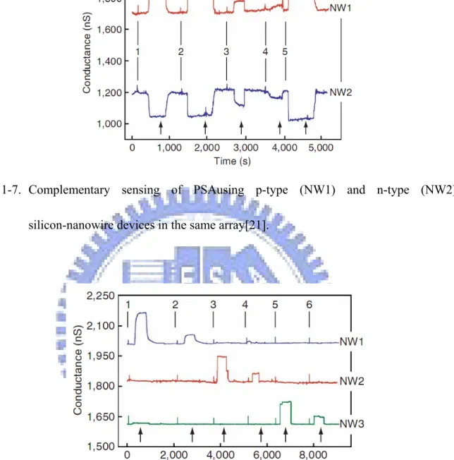
Recently, the same group demonstrated multiplexed, real-time, and label-free detection of cancer marker proteins, down to femtomolar concentrations, in a single platform[21]. SiNWs were aligned over a large area at the center of the chip by fluid-based assembly and formed more than 100 independently and electrically addressable arrays, which facilitate multiplexed detection. Fig. 1-6 shows the optical image of nanowire device arrays. Antibodies-modified SiNW sensors exhibited complementary response from p-type and
n-type nanowires (Fig. 1-7) and highly selective detection of prostate-specific antigen (PSA), bovine serum albumin (BSA), and mucin-1 simultaneously, as shown in Fig. 1-8. Furthermore, this device was capable of detecting PSA in undiluted serum sample, which only require a drop of blood and simple desalting process.
1.2.2.3 DNA detection
DNA detection is a very important area in biological science and technology. Gao and co-workers[22] fabricated highly ordered SiNW arrays by way of complementary metal-oxide-semiconductor (CMOS) compatible process involving deep ultraviolet lithography, dry etching, and self-limiting oxidation. Fig. 1-12 is the SEM, TEM, and AFM images of the highly uniform and perfectly aligned SiNW array. Besides, they demonstrated that peptide nucleic acid (PNA) functionalized SiNW arrays were capable of detecting complementary target DNA, and the resistance change was concentration-dependent, as shown in Fig. 1-13.
1.2.2.4 Virus detection
Virus sensors based on p-type SiNW was presented by Lieber and co-workers[23], and, most importantly, they demonstrated the capability of single virus detection. This experiment proved that nanowire-based sensors exhibit ultrahigh sensitivity. Fig. 1-11 shows the conductance (upper) and optical (lower) data that was recorded simultaneously from a nanowire device. When a single virus bound to a nanowire, a discrete conductance change
took place; the conductance returned to baseline value when the virus unbound from the nanowire. Moreover, selectivity and multiplexed detection were investigated in the experiment. With proper functionalization strategy and device design, Si nanowire devices were capable of distinguishing different viruses and detecting multiple viral species simultaneous. These results implies that SiNW-based sensors exhibit great potential for identification of viral families and could be a powerful tool for virology application.
1.3 Other nanowire sensors
1.3.1 Metal oxide nanowire sensor
Many groups successfully demonstrated chemical sensors based on semiconducting metal oxide 1-D nanostructures, including nanotube[24], nanorod[25], nanobelt[26], nanoribbon[27], and nanowire[28]. These are wire-like nanostructures and the electrical characteristics are greatly influenced by molecules adsorption or desorption at the surface. Various kinds of metal oxide wire-like nanostructures are reported, including ZnO, SnO2,
In2O3, Co3O4, Fe2O3, TiO2, MoO3, and V2O5. Among these, most attention has been focused
on ZnO, SnO2, and In2O3.
ZnO nanostructures in the form of nanorod, nanotube, and nanowire are reported, and all exhibit very high surface-to-volume ratio. Fan and Lu[29] developed a ZnO nanowire field-effect chemical sensor and investigated the sensing properties for NO2 and NH3. It’s
observed that gate potential can affect sensitivity, and applying a large negative gate voltage can desorb gas molecules at the surface, which is a alternative approach for sensor refreshing,
besides baking and UV illumination.
Moskovits and co-workers[30] investigated the O2 and CO sensing properties of SnO2
nanowire sensors and concluded that exposure to O2 created the surface acceptor states and
hence reduced the conductance, while exposure to combustible gases like CO led to oxidation-reduction reaction at the surface and reduced the surface oxygen concentration, increasing the conductance eventually. Afterward, they studied the interaction between surface reactivity and the electron density inside the nanowire, which is related to gate voltage[31]. And they confirmed that the rate and extent of oxygen ionosorption and CO oxidation reaction are controllable by applying different gate voltages[32].
Zhou’s group has done a series of studies on In2O3 nanowire sensors. First, they
demonstrated a NO2 and NH3 sensor that was based on a single In2O3 nanowire and operated
at room temperature[28]. The resistance of In2O3 nanowire changed by six and five orders of
magnitude as exposed to diluted NO2 and NH3 respectively, and the detection limits were
0.5ppm for NO2 and 0.02% for NH3. The response times were 5sec for 100ppm NO2 and
10sec for 1% NH3. Later, they explored the sensing mechanism by experimental
observations[33, 34]. They suggested that the oxygen vacancy doping effect was responsible for the Fermi level, EF, of In2O3 nanowires, and the direction of electron transfer was
determined by the value of EF and ENH3, the chemical potential of adsorbed NH3 molecules.
This explained different behaviors between devices. Fig. 1-14 shows the I-Vd curves and
energy band diagrams of heavily doped and lightly doped In2O3 nanowires. Continuously,
attributed this improvement to the nanowire/nanowire junctions between metal electrodes. Furthermore, they investigated the sensing behavior of In2O3 nanowire sensors for organic
molecules [36] and reported a new method for In2O3 surface functionalization that made In2O3
nanowire biosensors feasible.
1.3.2 Metal nanowire sensor
With proper plating solution, electrodeposition parameters, and the help of template, different kind of metal nanowires are successfully fabricated by many groups. After metal nanowire deposition, nanowires have to be transferred to device region and form reliable contact with electrodes. For nanowires made from ferromagnetic materials, if the nanowire is magnetized, the magnetic dipole lies along the wire’s axis because of the inherent shape anisotropy. Therefore, these magnetic nanowirs are orientable by applying magnetic field[37]. Application of magnetic alignment to segmented metal nanowires with ferromagnetic ends is demonstrated by Hangarter and co-workers[38]. Similarly, electric field is capable of polarizing and aligning nanowires. Electric field-assisted assembly of Au nanowires is demonstrated by Peter and co-workers[39].
Penner and co-workers[40] fabricated hydrogen sensors based on Pd nanowire array. Fig. 1-15 (A) and (B) is the schematic diagram of a palladium mesowire array (PMA) and the SEM image. The sensing mechanism is attributed to the conductivity increase based on hydrogen incorporation and microstructure change. AFM images of Pd nanowire before and after exposure to hydrogen gas are also shown in Fig. 1-15. Ag nanowire NH3 sensors are also
demonstrated by the same group[41].
Tao and co-workers[42] made use of Cu nanowire arrays to detect 2,2’-bipryidine(22BPY), adenine, and mercaptopropionic acid(MPA). They made the conclusion that the conductance modulation was the result of different surface scattering behavior and adsorbates-nanowire interactions, and the conductance change was specific for different adsorptions.
Wang and Ozkan[43] proposed a CdTe-Au-CdTe heterojunction nanowire DNA sensor. The schematic diagram of this segmented nanowire DNA sensor is shown in Fig. 1-16. The combination of semiconductor and metal achieves a field transistor configuration, which is more sensitive to surface charges than metallic nanowire. In addition, the Au segment benefits sensor performance by good functionalization capability of thiol-ended single strand DNA binding. In their experiment, complementary DNA solution at concentration as low as 1μM was detectable. The electrical characteristics at different concentrations are shown in Fig. 1-17.
1.3.3 Conducting polymer nanowire sensor
The material nature of polymer, such as mechanical flexibility and chemical diversity, leads to some advantages of conducting polymer nanowire(CPNW) sensors. By manipulation chemical reactions, we can fabricate CPNW with a wide range of conductivity, which is sensitive to surface adsorption of certain molecules due to doping or dedoping effect. Several methods of polymer nanowire fabrication are reported: electrochemical dip-pen
lithography[44], mechanical stretching[45], electrospinning[46], and template-directed electrochemical synthesis[47]. Generally speaking, CPNW is fabricated by way of electrochemical polymerization, and the positioning depends on template or position of electrodes.
Functionalization of CPNW can be carried out before, during, or after polymerization; that is, specific receptor is linked to monomer, involved in polymerization reaction[48], or reacts with fabricated polymer nanowire[49]. Moreover, physical entrapment of receptors is reported as a way of functionalization[50]. After functionalization, CPNW is capable of capturing target molecule and transduces binding events into electric signal.
Craighead and co-works[51] fabricated individual polyaniline/poly(ethylene oxide) nanowire sensors that successfully detect NH3 at concentration as low as 0.5ppm with short
response time and recovery time. Wang and co-works[52] proposed a new approach for in situ fabrication of individually addressable array of CPNWs within an integrated microfluidic device, and the sensor is ready to detect target molecule after polymerization. Ramanathan and co-works[53] demonstrated that CPNW sensor can be biomolecule-functionalized and achieve label-free DNA detecton. Fig. 1-18 shows the electrical responses of an unmodified nanowire (A) to 100 nM biotin-DNA (single stranded) and avidin-embedded polypyrrole (200 nm) nanowires to 1 nM (B) and 100 nM (C) biotin-DNA. The sensitivity ΔR/R is 13% at 1nM biotin-DNA.
However, CPNW is mechanically weak and hence not very reliable. Moreover, the harsh condition during CPNW synthesis may not be biocompatible, and postsynthesis assembly
remains a challenge.
1.3.4 Carbon nanotube sensor
Carbon nanotubes have drawn a lot of attention because of some unique features. First, single-walled nanotube (SWNT) has extremely small diameter (~1nm), which is comparable to the size of single bio-molecule. Furthermore, the fact that all the atoms of single-walled nanotube (SWNT) lie on the surface leads to high surface-to-volume ratio, and the curvature of surface maximizes the number of active sites. Finally, semiconducting nanotube has low carrier concentration inherently; therefore, the electrical characteristics are sensitive to charges adsorbed at the surface or delivered into nanotube. The geometrical nature and electrical property make carbon nanotube a promising building block for bioelectronic devices.
SWNTs can be synthesized by way of arc-discharge[54], laser ablation[55], gas-phase catalytic growth[56], and chemical vapor deposition[57]. Based on recent studies, gas-phase techniques turn out to be better approach for large-scale production with high purity.
Kong and co-workers[58] fabricated SWNT-based chemical sensors that exhibit fast response, high sensitivity, and capability of operating at room temperature. The conductance of SWNT sensors are decreased by two orders of magnitude by exposure to NH3 and
increased by three orders of magnitude by exposure to NO2.
Many applications of SWNT sensors on bioelectronics are also reported, including protein detection[59, 60], glucose detection[61], and DNA detection[62]. Heller and
co-workers[63] investigated the sensing mechanism of carbon nanotube biosensors and made the conclusion that electrostatic gating and Schottky barrier effects are two relevant mechanisms while electrostatic gating is more reliable and reproducible. Hence, passivation of metal contact regions is necessary for making reliable sensors.
1.4 SiGe nanowire IgG sensor
We have successfully fabricated SiGe spacer nanowire and demonstrated the ability of IgG antibody detection. Fig. 1-19 shows the mechanism of IgG detection. The functionalization procedure includes amino-propyl-trimethoxy-silane (APTMS) surface modification followed by bis-sulfo-succinimidyl suberate (BS3), which serves as a linker between APTMS and IgG antibody. Fig. 1-20 is the typical response of a SiGe IgG sensor that is based on a n-type nanowire. The conductance is modulated because of the fact that APTMS and IgG both induce positive charges, and BS3 induces negative charges at the surface in our experiment environment.
1.5 Sensitivity
Sensitivity of a nanowire-based sensor is defined as the ratio of the magnitude of conductance change to the baseline conductance value. Nanowire-based sensor exhibits higher sensitivity than conventional planar sensor mainly because of two reasons: (1) the surface-to-volume ratio is larger, and (2) the contribution of surface charges from sidewalls. Fig. 1-21 shows the simulated conductance values as a function of the surface potential for the
200-nm-wide and 50-nm-wide Si wires. Obviously, 50-nm-wide wire is more sensitive to surface potential.
Besides scaling, there are other strategies to improve sensitivity, such as material selection, surface engineering, structure engineering. According to Sberveglieri’s report[64], SnO2, ZnO, and In2O3 nanowires were all capable of ozone sensing, as shown in Fig. 1-22;
however, ZnO nanowires generated the lowest response despite the fact that the size of ZnO nanowire was the smallest in the experiment. This observation indicates that material selection is essential to sensitivity optimization. Au-nanoparticle-modified SiNW that proposed by Kun[65] is an example of surface engineering. The fact that Au provides better binding to thiol group at the surface is beneficial to functionalization. With regard to structure engineering, multi-segment CdTe-Au-CdTe nanowire proposed by Wang[43] is a typical example.
Considering semiconductor nanowires, such as Si and SiGe nanowires, it we treat them as cylindrical semiconducting channel in macro-scale with diameter d, length LNW, uniform
doping densityN , we can easily derive a simplified expression of conductance, conductance D
variation, and sensitivity respectively as follows[66]:
2 0 D / 4 NW G q N d L (1.1) / NW G d L (1.2) 4 D G S G qdN (1.3)rather simplified expression, we can still take it as a guideline for device design.
1.6 Motivation
The sensing mechanism of semiconductor nanowire is also called gating effect because it’s analogous to the operation of a MOSFET. Yeo and co-workers[67] reported that PMOSFET and NMOSFET with SiGe channel provided larger drain current than those with Si channel, as shown in Fig. 1-23. This result implies that SiGe may be a promising candidate for sensing application. In this study, we made n-type and p-type polycrystalline Si and SiGe nanowires to investigate the performance of different devices.
Moreover, based on the experimental results of Si and SiGe nanowires, we propose a novel structure to improve sensitivity: non-homogeneous structure. According to equation (1.1), (1.2), and (1.3), we can tell that the baseline conductance is determined by the bulk property of nanowire, and the conductance change depends on the surface chemistry and the electrical property of the outer region of nanowire. To achieve ultrahigh sensitivity, the conductance of nanowire must be as low as possible, and the conductance change must be as high as possible. Here we propose a novel structure engineering to satisfy both requirements at the same time: non-homogeneous structure, which is similar to the core-shell structure of some nanowires grown by bottom-up approach. In this study, SiGe with low Ge concentration serves as the core, and SiGe with high Ge concentration is the shell. By using this non-homogeneous structure, the conductance could be lowered while the surface remains sensitive. In this configuration, current tends to flow through the Ge-rich region because of
low resistivity and, therefore, the effective surface-to-volume ratio gets increased. In this thesis we utilize Ge condensation technique to obtain non-homogeneity because it offers full coverage of Ge-rich region and reduces the size of nanowire simultaneously.
1.7 Ge condensation technology
There are three ways to further reduce the size of as-fabricated Si nanowire: oxidation, anisotropic wet etching, and electrochemical method. Oxidation is widely used and very practical as a way of size reduction for Si nanostructure since it’s a extensively studied and well controlled process in VLSI technology. Oxidation of SiGe is also named Ge condensation because only Si is oxidized during oxidation, and Ge is rejected from pure SiO2
layer, increasing Ge concentration under oxide layer. This phenomenon is observed in 1980s[68] and receives a lot of attention since then owing to the importance of SiGe and Ge for electronic and optoelectronic devices[68].
Conventionally, in order to obtain SiGe film with high Ge concentration and good quality, it’s necessary to increase Ge concentration gradually during deposition, resulting in very thick SiGe film which is not practical. Several groups have demonstrated that ultrathin SiGe film with very high Ge concentration and good quality is attainable by way of Ge condensation. Recently, Ge condensation technology is employed to fabricate silicon germanium on insulator (SGOI) and even germanium on insulator (GOI). SGOI provides the same advantages as SOI, and SiGe layer can serve as channel material or induce strain to Si channel. Either way increases the carrier mobility, improves device performance, and helps meet the requirement of high speed circuit.
In our study, we utilize this technology to implement size reduction and at the same time raise Ge concentration, which greatly enhances sensitivity.
1.7.1 Oxidation behavior of SiGe
According to the ternary phase diagram of Si-Ge-O system at 1000℃, which is shown in Fig. 1-24, we can tell that as long as pure Si exists, no GeO2 is formed under equilibrium
condition. In real situation, the theoretical result is still available under certain condition. When Ge concentration is under certain critical value, only Si is oxidized during oxidation, and Ge is completely rejected from SiO2 and piles up at SiO2/SiGe interface. The thickness of
this Ge-rich region at interface depends on oxidation temperature and duration, which determine the Ge diffusion behavior. The critical concentration is reported to be 50% for single crystalline SiGe[69] and 40% for polycrystalline SiGe[70]. When Ge concentration exceeds the critical concentration, two oxide layers are formed during oxidation. At the initial stage of oxidation, both Si and Ge are oxidized, and the oxide layer is composed of (Si,Ge)O2.
After (Si,Ge)O2 is formed, oxygen has to diffuse through oxide layer to react with underlying
Si or Ge; therefore, oxidation rate slows down. When the oxidation rate is slow enough and the supply of Si is sufficient, the composition of second oxide layer becomes pure SiO2. The
formation of (Si,Ge)O2 is also observed when oxidation takes place at relatively low
temperature. This phenomenon leads to Ge loss and is undesirable.
Moreover, in case that the oxide layer on top of SiGe layer is not very thick, the presence of Ge enhances the oxidation rate of Si by a factor about 2~3 in wet oxidation and 1.5~2 in dry oxidation. Oxidation rate of SiGe film is correlated to Ge concentration; oxidation rate increases as Ge concentration is higher. This phenomenon is demonstrated for both single crystalline SiGe and polycrystalline SiGe in both wet ambient and dry ambient.
Besides, the effect of oxidation temperature and annealing are studied by several groups, aiming at obtaining high quality and high Ge concentration SiGe film. It’s demonstrated that defect free and strain relaxed Ge-rich SiGe film can be obtained.
1.7.2 Oxidation mechanism of SiGe
Many models are proposed to elucidate the oxidation mechanism of SiGe[71, 72]. Basically, it can be well explained by the combination of oxidation kinetics and diffusion kinetics.
Considering oxidation kinetics first, the reaction at the SiGe surface can be expressed by two equations[71]:
Si + O2 SiO2,
with Gibbs free energy change of ΔG1= -732 kJ/mol O2 and
Ge + O2 GeO2,
with Gibbs free energy change of ΔG2= -376 kJ/mol O2. Combing these two equations, we get
the third equation:
GeO2 + Si Ge + SiO2
with Gibbs free energy change of ΔG3= -356 kJ/mol O2. When SiGe is exposed to oxidizing
ambient, Si and Ge will be oxidized simultaneously. And Si is more reactive than Ge in oxidizing ambient according to these equations. Furthermore, we can tell from ΔG3 that any
Ge oxidized will eventually be reduced by Si, resulting in pure SiO2 and Ge pileup at
interface.
To explain the presence of (Si,Ge)O2, Si and Ge interdiffusion must be taken in to
consideration. During oxidation, Si diffuses outward to react with oxygen atom, and Ge diffuses inward because of concentration gradient. GeO2 may not be completely reduced if the
quantity of Si atoms at the surface is insufficient to consume all oxygen atoms; that is, Ge concentration is too high at the surface, or the temperature is too low for Si atom to diffuse upward fast enough. As oxide grows, oxidation rate slows down and Si quantity becomes sufficient; therefore pure SiO2 shows up beneath (Si,Ge)O2 layer.
The distribution of Ge under oxide layer is determined by diffusion kinetics. It’s observed that at higher oxidation temperature, Ge distribution becomes more uniform. Ge condensation comes along with strain and stress; therefore, Ge interdiffusion must be considered in order to avoid defect generation or even amorphorization.
The fact that SiGe shows higher oxidation rate than Si at the initial stage can be attributed to two reasons: (1)Si-Ge bond is weaker than Si-Si bond, (2)the reaction between Si and GeO is very fast, and (3)the presence of Ge greatly reduces Si interstitials injection during oxidation[72]. Lower binding energy means that it’s easier to break Si-Ge bond and form oxide than Si-Si bond. The difference of binding energy can’t fully explain this phenomenon, so other reasons is proposed. Ge tends to form GeO or GeO2, and both compounds can be
reduced by Si. It’s discovered that although it’s a two-step-process, SiO2 can be formed very fast through the reaction between GeO and Si, even faster than the reaction between O and Si. This provides a shortcut for SiO2 formation. Besides, point defect shows great impact on
oxidation rate. For Si oxidation, Si interstitials injection is a factor that reduce oxidation rate. However, Si interstitials injection is greatly alleviated with the presence of Ge. In addition, the vacancy flux from oxide to SiGe bulk is reported, which means more Si atoms diffuse to the interface through vacancy and react with oxygen atoms.
1.8 Thesis organization
This thesis is divided into six chapters. Chapter 1 introduces general background of nanowire-based sensors, motivation of this study, and Ge condensation technology. Chapter 2 describes process flow of nanowire fabrication, device structure, and the method of electrical characteristics measurement. In Chapter 3, experimental results of SiGe and Si nanowire sensors are presented and discussed. In Chapter 4, fabrication and electrical characteristics of
non-homogeneous SiGe nanowire are investigated. Conclusion is made in Chapter 5, and some proposals for future work are given in Chapter 6.
Chapter 2
Experiment
Top-down approach was used for SiGe and Si nanowires fabrication in this study. Instead of commonly used e-beam lithography, we made use of spacer formation to obtain SiGe and Si spacers on nanometer scale, namely, SiGe and Si nanowires. Ge condensation technique was utilized to increase the Ge concentration in SiGe nanowires and reduce the size simultaneously.
2.1 Process flow
A p-type (Boron doped) Si substrate (100) was used in this study. The resistivity of the silicon substrate was about 1~10 Ω-cm. Samples were prepared by following processes: 1. Standard RCA clean and wet oxidation for about 6 hours at 980°C to grow 5000Ǻ thick
bottom oxide by ASM/LB45 furnance system. The structure is shown in Fig. 2-1.
2. Mask #1: Define active area. TEL CLEAN TRACK MK-8 and G-line lithography system were employed to transfer pattern onto oxide layer. Then, dry etching was carried out with TEL5000 R.I.E. system to form oxide step, which is 3000 Ǻ high and ready for sidewall spacer formation. The structure is shown in Fig. 2-2.
3. After standard RCA clean, 150Å α-Si layer was deposited on bottom oxide at 650°C for ~2 hours by ASM/LB45 furnance system. This α-Si layer served as seed layer for SiGe film deposition. The structure is shown in Fig. 2-3. This step was skipped for Si
nanowire fabrication.
4. After standard RCA clean, either poly-crystalline SiGe film was deposited by ANELAVA
SiGe UHV-CVD at 665°C, or poly-crystalline Si film was deposited by ASM/LB45
furnance system. The structure is shown in Fig. 2-4.
5. Mask #2: Define S/D region and form spacer. Dry etching was carried out with TCP9400
SE poly etcher to remove unwanted part of active layer. Only the S/D region and SiGe or
Si nanowires were retained. The structure is shown in Fig. 2-5.
6. Mask #3: Remove unwanted sidewall spacer. TCP poly etcher was employed to remove unwanted spacer, which would have resulted in short circuit between two nanowire devices if not removed. The structure is shown in Fig. 2-6.
7. Phosphorus (P) or boron-fluoride (BF2) ion implantation. The implantation dose is varied
from 1×10¹⁵ to 3×10¹⁵ ions/cm2. Implantation energy was from 15keV to 30keV for P+ implantation, 50keV for BF2+ implantation.
8. Annealing in furnace at 900°C for 30min to activate dopants. 9. 3000Ǻ Aluminum deposition by thermal coater
10. Mask #4: Define aluminum contact pad. Al pads are formed by wet etching (HNO3:CH3COOH:H3PO4:H2O=2:9:50:10). The structure is shown in Fig. 2-7.
11. Al sintering at 400℃ in N2 ambient for 30 minutes.
2.2 Functionalization
oxide layer around nanowires. Hydroxyl functional groups on the surface of native oxide layer were replaced by the methoxy groups of APTMS molecules. After APTMS modification, the surface of nanowire was terminated by amine groups. In our experimental environment, amine groups were prone to be positively charged; that is, the surface potential nanowire increased, and the conductance of n-type (p-type) nanowires increased (decreased). Next, we used bis-sulfo-succinimidyl suberate (BS3) as linker between APTMS and IgG antibody. BS3 treatment resulted in negative charges. Hence, the conductance of n-type (p-type) nanowires decreased (increased). After APTMS and BS3 modification, nanowires were capable of capturing IgG antibody. Our group has already demonstrated IgG sensing capability of SiGe nanowire sensor. In this study, we focused on investigating the change of conductance (ΔG) and sensitivity (S) of different samples under identical surface condition. Comparison was made by using ΔG and S corresponding to APTMS treatment since the situation became more complex, and the variation of experimental data was larger after BS3 treatment.
2.3 Measurement of electric characteristics
HP4156A was used in this study to measure the electric characteristics of nanowire
sensors. Drain voltage (VD) was varied from -8V to 8V and 200mV a step, and back gate
voltage (VG) was 0V. The measurement of electric characteristics was performed at every
stage of surface modification, and the average conductance was then extracted from ID-VD
Chapter 3
SiGe and Si Nanowire Sensors 3.1 Cross-section view of poly-crystalline SiGe and Si nanowires
Si0.8Ge0.2 and Si nanowires were successfully fabricated by sidewall spacer formation.
Fig. 3-1 and Fig. 3-2 are the SEM images of Si0.8Ge0.2 and Si nanowires respectively. The
average height of Si0.8Ge0.2 nanowire was 175nm, and the average width was about 60nm.
The average height and width of Si nanowire were about 160nm and 90nm respectively. According to SEM images, the surface area of Si0.8Ge0.2 nanowire was close to that of Si
nanowire, and the volume of Si0.8Ge0.2 was smaller than that of Si nanowire.
3.2 Electrical characteristics of SiGe and Si nanowire sensors before and after APTMS and BS3 modification
Both p-type and n-type nanowires were fabricated. Fig. 3-3 is the ID-VD characteristics of
a p-type Si0.8Ge0.2 nanowire device, which is 13μm in length. Normal denotes the data recorded
from the blank nanowire. Conductance extracted from ID-VD characteristics is shown in Fig. 3-4.
After APTMS modification, the conductance of this p-type Si0.8Ge0.2 nanowire device decreased
because APTMS molecules were positively charged. Then the p-type Si0.8Ge0.2 nanowire
underwent BS3 modification, and the conductance increased simultaneously since BS3 molecules possessed negative charges. The ID-VD characteristics and conductance of a n-type
nanowire was 8μm. The n-type Si0.8Ge0.2 nanowire exhibited opposite behavior to p-type
nanowire. The conductance of n-type Si0.8Ge0.2 nanowire increased after APTMS modification
and decreased after BS3 treatment. This complementary sensing behavior was consistent with the fact that APTMS molecules were positively charged, and BS3 molecules were negatively charged. Moreover, complementary conductance changes verified that the response of Si0.8Ge0.2 nanowire sensor was indeed the result of specific binding of APTMS molecules and
BS3 molecules. Besides, the capability of complementary sensing is important because signals due to electrical noise and non-specific binding could be filtered off if we fabricated both n- and p-type SiGe nanowires on the same chip.
The ID-VD curves and conductance of a 9μm-long p-type Si nanowire are shown in Fig.
3-7 and Fig. 3-8 respectively, and the electrical characteristics of a 17μm-long n-type Si nanowire are shown in Fig. 3-9 and Fig. 3-10. The ID-VD curves of these devices were all
linear, which indicated that it was ohmic contact between Al electrodes and Si0.8Ge0.2 or Si.
Sensing behavior of Si nanowires was similar to that of SiGe nanowires.
To clarify the difference between SiGe and Si nanowires, the change of conductance (ΔG ) of several nanowires on each chip after APTMS modification were shown in Fig. 3-11. In our experiment, nanowires with length in a range from 3μm to 50μm were fabricated in a chip. In order to compare ΔG between nanowires, we normalized ΔG by multiplying ΔG and the length of nanowire (LNW) together. According to Nair’s simulation results[66], the length of
nanowire was reported as a factor of sensitivity; however, the impact of length variation on sensitivity should be neglectable in our experiment because a large amount of positive charges
were induced by APTMS modification and covered entire nanowire.
Complementary sensing is clearly seen in Fig. 3-11. P-type Si0.8Ge0.2 and Si nanowires
exhibited negative conductance change while the conductance change of n-type nanowires was positive. Average ΔG of p-type Si0.8Ge0.2 nanowires was the greatest in magnitude among
all samples. It was 74% larger than the ΔG of p-type Si. As for n-type Si0.8Ge0.2 and Si
nanowires, ΔG of n-type Si0.8Ge0.2 was 36% larger than that of n-type Si. Both p-type and
n-type Si0.8Ge0.2 nanowires provided larger ΔG than Si nanowires. According to Equation
(1.2), since the surface areas of Si0.8Ge0.2 and Si nanowires were very close, there were two
possible reasons for this phenomenom: higher surface charge density or higher carrier mobility in Si0.8Ge0.2 nanowire. Surface charge density is related to the difference of surface
chemistry between SiGe and Si nanowires. Si-OH and Ge-OH groups co-existe at the surface of SiGe nanowire while there is only Si-OH groups on the surface of Si nanowire. Afer silanization reaction, the number of APTMS molecules binding on surface is likely to be different between SiGe and Si nanowires.
Besides, we observed that p-type nanowires generated larger ΔG than n-type nanowires. It’s attributed to the difference between depletion and accumulation. Nanowires operating in depletion mode exhibit larger ΔG than those in accumulation mode[66]. In this experiment, APTMS modification led to depletion for p-type nanowires and accumulation for n-type nanowires.
Fig. 3-12 shows the baseline conductance (G0) of SiGe and Si nanowires. Although the
nanowires was much larger. This result may be duo to higher degree of dopant activation or higher mobility in p-type nanowires. Higher hole mobility is considered as the main reason that p-type SiGe nanowires exhibited much higher conductance than p-type Si[73-75]. The baseline conductance values of n-type SiGe and Si nanowires were about the same. Since the volume of Si nanowires was slightly larger, dopant activation and electron mobiliy were likely to be promoted in SiGe nanowires.
The conductance change corresponding to BS3 molecule binding of APTMS-modified nanowires depends on the number of APTMS molecules on the surface of nanowire. We estimated the percentage of BS3-linked APTMS molecules from the ration of ΔG. 30~60% APTMS molecules on the surface of nanowires were bound to BS3 molecules in our experiment. It’s impossible to link every APTMS molecule to BS3 molecule because of electrostatic repulsive force. The optimum modification condition requires further investigation.
3.3 Sensitivity of Si0.8Ge0.2 and Si nanowire sensors to APTMS
Fig. 3-13 shows the sensitivity (S) of Si0.8Ge0.2 and Si nanowire sensors. Although p-type
Si0.8Ge0.2 device generated the largest ΔG, the sensitivity of p-type Si0.8Ge0.2 device was the
lowest because the baseline conductance was much larger than other devices. N-type devices exhibited higher sensitivity than p-type devices because of smaller baseline conductance. N-type Si0.8Ge0.2 device had the highest sensitivity (20.5%) in our experiment. These results
p-type Si nanowire sensor exhibited higher conductance and conductance change. However, n-type sensor provided larger sensitivity.
3.4 Conductance change and sensitivity of blank nanowires to DI water and BS3
We also treated as-fabricated Si0.8Ge0.2 and Si devices with deionized (DI) water and
recorded the change of conductance, which is shown in Fig. 3-14. The conductance of nanowires tended to increase after DI water treatment. Possible causes of this result includes non-intentional binding, passivation effect[77], pH variation, contamination of container, and impurities in DI water. However, the magnitude of ΔG was much smaller than the response to APTMS binding.
The response of blank nanowires to BS3 solution is shown in Fig. 3-15. The conductance of p-type Si0.8Ge0.2 nanowires decreased while other nanowires generated both negative and
positive ΔG. Conductance variation of blank nanowires after BS3 treatment was attributed to non-specific binding. It’s much smaller than the response of as-fabricated nanowires to APTMS molecules and the response of APTMS-modified nanowires to BS3 molecules.
Fig. 3-16 ~ 3-19 show the summary of sensitivity of p-type Si0.8Ge0.2, n-type Si0.8Ge0.2,
p-type Si, and n-type Si nanowires respectively. The fact that sensitivity to APTMS molecules was apparently higher than to DI water and BS3 proved that the conductance changes shown in Fig. 3-11 were indeed resulted from specific binding of APTMS molecules, and APTMS modification was necessary for BS3 binding.
Chapter 4
Non-homogeneous SiGe Nanowire Sensors 4.1 Achieving non-homogeniety by dry oxidation at 900℃ for 4 minutes
Si0.93Ge0.07 nanowires were used in this experiment. The width of nanowires was about
75nm, and the height was about 210nm. In order to obtain Ge-rich layer at the outer region of nanowires, Si0.93Ge0.07 nanowires underwent dry oxidation at 900℃ for 4 minutes. We set the
oxidation temperature at 900℃ to suppress inward diffusion of Ge atoms, aiming at confining Ge atoms at the outer region of nanowires. After oxidation, the width of nanowires was around 55nm, and the height of nanowires was about 190nm. Fig. 4-1 is the SEM image of one of the nanowires after oxidation. The undercut below the nanowire was due to the underlayer oxide etching during wafer cleaning. Fig. 4-2 is the Auger depth profile after oxidation. Although the real Ge concentration can’t be measured because of the lack of standard sample for calibration, it’s obvious that Ge concentration at the surface was greatly increased after oxidation, and SiGe was clearly divided into two layers according to concentration difference. Through this oxidation process, we successfully obtained non-homogeneous SiGe nanowire.
4.2 Electrical characteristics of Si0.93Ge0.07 nanowires after oxidation
Fig. 4-3 is the ID-VD characteristics of 8-μm-long nanowire. The curves were still linear
After APTMS modification, we observed 10% conductance change.
4.3 Effect of annealing on conductance change
A lot of articles regarding Ge condensation technology reported that Ge pile-up and defects generation are concomitant events during SiGe oxidation[78]. Therefore, we carried out in-situ annealing after oxidation to investigate the effect of annealing after oxidation. SiGe nanowires were in-situ annealed in N2 ambient at 1000℃, 900℃, and 700℃. Fig. 4-5 is the
schematic representation of oxidation and annealing process. After that, samples underwent phosphorus-ion implantation with the does of 3x1015cm-2. The ion energy was 15keV. We utilized RTA process as dopant activation for this experiment to prevent diffusion of Ge atoms; samples were annealed at 900℃ for 30 seconds.
First, we investigated the effect of 1000℃ annealing. ΔG of samples that were annealed for 5 minutes and 10 minutes, and without annealing are shown in Fig. 4-6. It was observed that ΔG of samples experienced 1000℃ annealing was smaller than that of the sample without annealing, and the performance of the 10-minute annealed sample was worse than that of the 5-minute annealed sample. We attribute this phenomenon to the diffusion behavior of Ge atoms. Fig. 4-7 is the Auger depth profile of Si, Ge, and O for the 10-minute annealed sample respectively. Ge diffusion became prominent at 1000℃, and Ge atoms diffused away from surface after 1000℃ annealing; therefore Ge-pileup was not observed in Fig. 4-7. Since oxide layer is considered as diffusion barrier for Ge atoms, out-diffusion could be ignored, and therefore the Ge diffusion is mainly from surface to the bulk of nanowires. After 10-minute
annealing at 1000℃, Ge distribution was quite uniform as shown in Fig. 4-7. Since Ge concentration near the surface was lowered after annealing at 1000℃, the conductance change caused by APTMS modification was lowered as well.
The effects of annealing at 900℃ and 700℃ were also investigated. ΔG of samples underwent 10-minute and 30-minute annealing at 900℃ and 60-minute annealing at 700℃ are plotted in Fig. 4-8. Since the Ge diffusion was very slow at 900℃, there was no sensitivity degradation after 900℃ annealing. On the contrary, ΔG was increased after annealing. This is attributed to the fact that defects that were generated during Ge condensation were healed out by annealing process, and the quality of the outer layer of nanowires was improved. As a result, the change of conductance was increased. Annealing for 30 minutes led to greater improvement than annealing for 10 minutes because more defects were healed. Fig. 4-9 is the Auger depth profile after annealing at 900℃ for 30 minutes. The Ge-rich region was slightly broader than that before annealing. Instead of spreading uniformly over the nanowire, which was the case of 1000℃ annealing, annealing at 900℃ for 30 minutes made the Ge distribution become locally uniform while maintaining Ge-rich layer next to the surface. Annealing at 700℃ for 60 minutes also resulted in greater response because Ge atoms barely diffused inward, and some defects were recovered. However, 700℃ annealing was insufficient for healing all defects; namely, some defects could only be recovered at higher temperature when more energy is provided. Therefore, the response of nanowires annealed at 700℃ for 60 minutes was slightly greater than that of nanowires annealed at 900℃ for 10 minutes but still smaller than the conductance change of nanowires annealed at 900℃ for 30
minutes.
4.4 Effect of annealing on conductance of nanowires
Fig. 4-10 shows the conductance of samples underwent different annealing process. In our experiment, there is no direct relationship between conductance and annealing process. Our explanation is that the size of nanowire is the dominant factor of conductance for wires in this scale. However, the oxidation process is difficult to control since nanowires we fabricated are polycrystalline, and oxidation of SiGe is very fast. Besides, the uniformity of the thickness of Si0.93Ge0.07 film deposited by UHVCVD also has great impact on conductance. We believe
that the variation of conductance is the result of size variation from SiGe deposition and oxidation. Since conductance is related to the cross-section area that could be estimated by the product of width and height of nanowire in our experiment, it is greatly influenced by size variation.
4.5 Annealing at 900℃ for 30 minutes after ion implantation
In order to simplify thermal processes, we carried out 900℃ annealing as dopant activation instead of in situ annealing. Fig. 4-11 shows normalized ΔG of A and B sample. A sample was in situ annealed at 900℃ for 30 minutes after oxidation, and B sample was not in situ annealed but instead underwent 30 minutes 900℃ annealing after ion implantation. ΔG of B sample was about 25% larger than that of A sample. This improvement was attributed to the distribution of phosphorus atoms. After phosphorus ion implantation, both A and B sample
underwent 900℃ annealing. A sample and B sample were annealed for 30 seconds and 30 minutes respectively. Since the implantation energy in this experiment was quite low, the peak of phosphorus atom distribution in A sample was very close to the suface. As for B sample, diffusion of phosphorus atoms was more prominent, and the concentration of phosphorus at the surface was lowered. Consequently, electron mobility and ΔG increased.
Conductance of A and B sample was about the same, as shown in Fig. 4-12. Annealing at 900℃ for 30 minutes is likely to cause more dopant segregation at grain boundaries and more out-diffusion; hence, conductance did not increase for longer duration of annealing. Sensitivity of A sample and B sample were 21%, and 25.5% respectively.
According to our observation, annealing at 900℃ for 30 minutes as dopant activation always led to higher ΔG than rapid thermal annealing. However, in some cases, nanowires that underwent 30 minutes annealing exhibited higher conductance and, hence, lower sensitivity. It depends on doping types, annealing temperature, and annealing duration.
4.6 Estimation of surface charge density
The capacitance between Al electrode and back gate was 2.175x10⁻⁸F/cm2, and the surface charges that led to 25.5% conductance change in B sample was equivalent to about 136V back gate voltage according to ID-VG characteristics. If we use the equation Q=CV to
estimated surface charge density, the number of surface charge density would be
1.85x1013cm-2. Compared to the number of active site on Si native oxide, ~5x1014 cm-2[79], the value of surface charge density is reasonable.

![Fig. 1-1. Numerical simulation result of the relationship between the response time (ts) and the detectable concentration (ρ0) of a DNA sensor[1]](https://thumb-ap.123doks.com/thumbv2/9libinfo/8755685.206848/56.892.284.654.103.399/numerical-simulation-result-relationship-response-detectable-concentration-sensor.webp)