IEEE TRANSACTIONS ON ELECTRON DEVICES, VOL. 42, NO. 6, JUNE 1995 1141
Modeling the Positive-Feedback Regenerative
Process of
CMOS
Latchup by a Positive Transient
Pole Method-Part
I: Theoretical Derivation
Ming-Dou Ker, Member, IEEE, and Chung-Yu Wu, Member, IEEE
Abstract- A novel method to characterize the mechanism of positive-feedback regeneration in a p-n-p-n structure during CMOS latchup transition is developed. It is based on the de- rived time-varying transient poles in large-signal base-emitter voltages of the lumped equivalent circuit of a p-n-p-n struc- ture. Through calculating the time-varying transient poles during CMOS latchup transition, it is found that there exists a transient pole to change from negative to positive and then this pole changes to negative again. A p-n-p-n structure, which has a stronger positive-feedback regeneration during turn-on transi- tion, will lead to a larger positive transient pole. The time when the positive transient pole occurs during CMOS latchup transi- tion is the time when the positive-feedback regeneration starts. By this positive transient pole, the positive-feedback regenerative process of CMOS latchup can be quantitatively characterized.
NOMENCLATURE
Parasitic lateral (vertical) p-n-p (n-p-n) BJT in a p-n-p-n structure of CMOS latchup. Equivalent substrate (well) resistances in CMOS IC’s.
Base-emitter junction depletion capacitance of BJT Q i ( Q 2 ) .
Base-collector junction depletion capacitance of BJT Q1(Q2).
Base-emitter junction diffusion capacitance of BJT Qi(Q-2).
Base-collector junction diffusion capacitance of BJT Ql(Q2).
Base-emitter junction capacitance of BJT
Ql(Q2) including depletion and diffusion capacitances as defined in (8) or (10). Base-collector junction capacitance of BJT Q1 ( Q 2 ) including depletion and diffusion capacitances as defined in (9) or (11). Transient-induced trigger current generated in substrate (well) to cause CMOS latchup. Voltage-dependent intrinsic base current of BJT Ql(Q2) without the displacement current of capacitances.
Manuscript received September 7, 1994. The review of this paper was arranged by Associate Editor K. Tada. This work was supported by United Microelectronics Corporation (UMC), Taiwan, ROC, under Contract C8205 1. The authors are with Integrated Circuits and Systems Laboratory, Institute of Electronics and Department of Electronics Engineering, National Chiao- Tung University, Hsin-Chu, Taiwan 300, Republic of China.
IEEE Log Number 9410585.
Voltage-dependent intrinsic collector current of BJT Ql(Q2) without the displacement
current of capacitances.
Large-signal base current of BJT Ql(Q2)
including the displacement current of capacitances as defined in (4) or ( 6 ) .
Large-signal collector current of BJT
Q1 (Q2) including the displacement current
of capacitances as defined in (5) or (7). Large-signal base-emitter voltage of BJT
Qi(Q2).
Large-signal base-collector voltage of BJT
Q i ( Q 2 ) .
Power supply of CMOS IC’s. _ - - Piecewise-linearized large-signal transconductance of base current with respect to its base-emitter voltage of BJT
Q i ( Q 2 ) .
Piecewise-linearized large-signal transconductance of collector current with respect to its base-emitter voltage of BJT
Q i ( Q 2 ) .
A certain time interval during CMOS latchup transition.
Poles of the solved time-dependent V E B ~ ( ~ ) and wgEz(t) as defined in (21) and (22). Maximum peak value of the positive p l pole during latchup transition.
The time required for pl pole to become positive after trigger currents are applied.
I. INTRODUCTION
S CMOS technology is scaled down to submicron regime
A
to achieve higher integration density and faster operation speed in VLSVULSI applications, the reduced spacings of the inherently embedded parasitic p-n-p-n structure further increase the latchup susceptibility of CMOS IC’s. Latchup, which creates a low impedance path from the power supplyVDD to ground, is one of major failure mechanisms in the reliability of bulk CMOS IC’s. The dc switching voltage of a parasitic p-n-p-n structure designed according to the design rules and fabricated by the submicron bulk CMOS technology is as high as 30-50 V, which is much greater than 5 volt of VDD power supply in CMOS IC’s. Thus, latchup in CMOS IC’s is initially triggered by sharp voltage/current transitions
1142 IEEE TRANSACTIONS ON ELECTRON DEVICES, VOL. 42. NO. 6, JUNE 1995
or by voltage/current overshooting and undershooting at the power supplies or at the output nodes, rather than by direct overstress of dc voltage. This transient-induced latchup is especially acute in CMOS IC's because short-circuit currents only during logic switching transitions, which usually Cause voltage overshooting or undershooting at the clock transition edges.
regenerative I-V characteristics in a p-n-p-n structure, it is more difficult to model latchup in the transient case with the additional variable of time than in the dc case. Latchup firing is in itself a transient phenomenon, so it has to be discussed in time domain. The latchup transition and its mechanisms have attracted much attention, and some efforts have been
improve the immunity against transient-induced latchup in CMOS IC's.
11. DYNAMIC BEHAVIORS OF CMOS LATCHUP TRANSITION The classical two-transistor model of a p-n-p-n structure with device parameters extracted from the fabricated p-n-p-n structure in CMOS IC's is adopted to analyze the dynamic parameters including current-dependent beta gain, voltage- dependent junction capacitance, and transit time, it can offer
a reasonable accuracy in modeling the process of a
P-n-P-n structure.
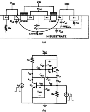
Fig. l(a) shows the schematic cross-sectional view of a CMOS inverter and the parasitic p-n-p-n latching path in the Due to the phenomena Of cross-coupled behaviors of CMOS latchup transition. With extracted device
contributed to characterize it [l]-[l91. In the transient behaviors Of
past, the process in the thyristor Or
p-well n-substrate bulk CMOS technology. The corresponding lumped equivalent circuit of the p-n-p-n structure is shown the semiconductor-controlled-rectifier (SCR) had also been
characterized [20]-[30].
there are two main approaches
in Fig. l(b), where Q1 ( Q 2 ) is the parasitic lateral
p-n-p (n-p-n) bipolar junction transistor (BJT). Q1 transistor is composed of p+ diffusion as emitter, n-substrate as base, In the previous
to and p-well as its collector. Q2 transistor is composed of
the Of based On the l u m p d n-substrate as collector, p-well as base, and n+ diffusion
the application of Of a
latchup behavior in a p-n-P-n One is
equivalent circuits [11-[131, [201-[231, [311-[381. n e other is in p-well as its emitter. Resistor R ~ ( R ~ ) is the equivalent based on the substrate (well) resistance. The voltage-dependent base-emitter and base-collector junction capacitances (Gel, C e z , eel, and set Of semiconductor device equations with process
parameters 1141-1191, [26]-[30],[39]-1411. The lumped equiv- Cc2) are also shown in Fig. l(a) and (b). The transient-
alent induced trigger currents generated in n-substrate and p-well
latchup transition. Some had been to judge by internal voltage/current transitions due to circuit operations [2l19 [3lI-[371.
is Often to study the switching behaviors Of
the occurrence of latchup in a p-n-p-n Structure [9l-[l3]? [2019 more accurate representation of 2-D or 3-D p-n-p-n structure and the detailed dynamics of charge distribution during latchup transition. But, numerical simulation demands much comput- ing resource and often offers little analytical understanding on latchup transition. The restriction to finite representation of a p-n-p-n structure and the lack of general latchup criterion also make the numerical simulation approach somewhat inefficient. Analytical model with a general latchup criterion is still quite helpful in understanding and controlling latchup for practical and efficient applications. It can provide us with good design guidelines and quick initial characterization. Then numerical simulation can be used as a refining treatment.
In the literatures describing latchup transition, the switch- impedance) state to its ON (low-impedance) state are all described qualitatively. No any method is developed to quan- a p-n-p-n structure and used to characterize the positive- parameters.
rived from the large-signal behaviors of a p-n-p-n structure and CMOS latchup transition. By using this time-varying positive transient pole, the switching mechanism of a p-n-p-n structure can be well explained and fully characterized. Especially, the influences of device parameters on the positive-feedback
or by external voltage/current transitions due to unexpected currents, respectively.
among the large-signal branch
approach may offer events to cause CMOS latchup are marked as the Il and
I z
Through the circuit connection in Fig. l(b), the relations and node voltages are (1) (2) (3) Talung the effects of junction depletion and diffusion ca- pacitances into considerations and using the modified Gum- mel-Poon model of BJT [421-[441, the large-signal base and written asw E B l (t> =
i C Z ( t )
+
Il(t) - i B l ( t ) -7
i C l ( t )+
I z ( t ) - i B Z ( t ) -7
~ B E Z ( ~ ) = 0 v c B l ( t ) = v B C z ( t ) = -['OD - v E B l ( t ) - wBE2(t)l.ing mechanism Of a p-n-p-n structure from the OFF (high- collector currents of BJT's Q1 and Q z in Fig. l(b) can be
(4) ( 5 ) ( 6 ) (7) a ( C e 1 . V E B ~ ) + a ( c c 1 . v c B 1 )
at
titatively investigate the mechanism of turn-on process infeedback regeneration of latchup transition in terms of device In this paper, a time-varying positive transient pole is de- used to analyze the positive-feedback regenerative process of
i B l ( t ) = I B l ( t )
+
at i C l ( t ) = I C l ( t ) - at i B 2 ( t ) =IBZ(t)+
at
icz(t) = ICZ(t) -at
a ( C c 1 ' uCB1) a ( c e z.
~ B E Z ) + a ( C c 2 . ~ B C Z ) a ( c c 2 . u E C 2 )at
where (8) (9) (10) c e l = C j b e l+
C r b e lregeneration of CMOS latchup transition can be quantitatively investigated. Therefore some guidelines can be obtained to
c c l = C j b c l -k Crbcl c e 2 = CjbeZ
+
CrbeZKER AND WU: MODELING THE POSITIVE-FEEDBACK REGENERATIVE PROCESS OF CMOS LATCHUP-PART I 1143 Latchlng pth N-SUBSTRATE vaut Latchlng pth N-SUBSTRATE (b)
Fig. 1. (a) A schematic cross-sectional view of a CMOS inverter and the parasitic resistances and capacitances in a p-n-p-n structure; (b) The lumped equivalent circuit of the p-n-p-n structure in (a).
c c 2 = Cjbc2 C r b c Z . (1 1) From the above equations, it is obviously indicated that the tum-on mechanisms of a p-n-p-n structure are heavily dependent on its junction capacitances.
The intrinsic base and collector currents of BJT's are exponential functions of their base-emitter and base-collector voltages. The junction capacitances are also related to their base-emitter and base-collector voltages [42]-[44]. In (3), the base-collector voltages of BJT's Q1 and Q 2 in the lumped equivalent circuit of Fig. l(b) can be expressed in terms of their base-emitter voltages. Thus, the time-varying large- signal base-emitter voltages, V E B l ( t ) and V B E 2 ( t ) , are the most fundamental factors in the lumped equivalent circuit of a p-n-p-n structure during its turn-on transition. If these V E B ~ ( ~ ) and V g E 2 ( t ) are solved, all branch currents and node voltages of the lumped equivalent circuit in Fig. l(b) can be found out from them.
In order to observe the time dependence of latchup transi- tion, the popular circuit simulator HSPZCE [44] is adopted to accurately solve these V E B ~ (t) and V B E Z ( t ) . With extracted device parameters of parasitic lateral and vertical BJT's in a p-n-p-n structure as listed in Table I, V E B l ( t ) and wBEz(t) in both latchup and nonlatchup cases triggered by a pulse-type 5-mA substrate current 11 with two different pulse widths of 10 nS and 3.5 nS are simulated by HSPZCE and the results are drawn in Fig. 2. The equivalent substrate and well resistances
(Rs
andRw)
used in the simulation are 800O and 5.6 KO, respectively. The 5-mA 11 pulse is applied at the time interval o f t = 0. Before t = 0, V E B ~ ( ~ ) and V B E Z ( t ) are set to zero42 R.=800n, Rw-S.6KR.
4 A
10 P a 40
Time (nS)
Fig. 2. The typical HSPICE simulated f f ~ ~ l ( t ) and f f B E Z ( t ) waveforms of a p-n-p-n structure with Rs = 8000 and R w = 5.6K0 in both latchup and nonlatchup cases.
TABLE I
AND VERTICAL BJT's IN A p-n-p-n STRUCTURE OF CMOS IC's THE EXTRACTED DEVICE PARAMETERS OF THE PARASITIC LATERAL
parameter Q1( PU-P 1 4 ( n ~ n ) ( l a t e r a l ) (vertical) 1.104 0.2 2.8333-16 6.909M 4.2503-14 20 10 2.0 277.2 2.0 8.1123-16 4.867E-4 1.2173-13 0.25 2.0 0.6 Cjeo(PF) 0.6 1.3 MJE 0.5 0.5 MJC 0.33 0.33
because the p-n-p-n structure is initially
08.
As the 5-mA 11is applied with 10-nS pulse width, u E B l ( t ) raises up quickly in several nanosecond (nS) and then holds on a stable value about 0.827 V, while v g ~ z ( t ) first drops to -0.345 V and then raises up and holds on about 0.897 V. After 11 trigger current changes from 5 mA to 0 mA at the time interval of 10 nS, V E B ~ ( ~ ) and V B E ~ ( ~ ) still remain in their stable values, and this condition is the latchup case. On the contrary, if the 5-mA 11 trigger current only with 3.5-11s pulse width, V E B l ( t ) and W B E ~ ( ~ ) are first raising as those in the latchup case but then they drop to zero volt after 11 triggering. Since V E B l ( t ) and W g E 2 ( t ) cannot hold on their stable turn-on voltages after triggering, this is a nonlatchup case. If the pulse width of the 5-mA 11 trigger current is reduced from 10 nS to 3.5 nS, it can be found that there is a minimum value of pulse width to sustain the occurrence of latchup. Similarly, variations of V E B ~ ( ~ ) and ~ g ~ z ( t ) due to well current 1 2 triggering can be also observed by this method. Generally, a trigger current with higher pulse amplitude requires a shorter minimum pulse width to initiate the occurrence of CMOS latchup [13].
Through observation on V E B ~ ( ~ ) and Vp,EZ(t), the dynamic behaviors of CMOS latchup transition due to transient-induced substrate or well currents triggering can be clearly understood.
1144 IEEE TRANSACTIONS ON ELECTRON DEVICES, VOL. 42, NO. 6, JUNE 1995
In this work, the efforts are emphasized to quantitatively model the positive-feedback regenerative process of CMOS latchup and to investigate the influence of device parameters on this positive-feedback regeneration in a p-n-p-n structure.
111. THE TIME-VARYING POSITIVE TRANSIENT POLE
AND ITS EFFECT ON CMOS LATCHUP TRANSITION Traditionally, the positive-feedback regenerative process during latchup transition in a p-n-p-n structure is qualitatively explained as the regeneration in cross-coupled base and col- lector currents of BJT's Q1 and Q2 with the sum of their alpha
gains or the product of their beta gains greater than unity [45], [46]. In Section 11, V E B ~ ( ~ ) and W B E ~ ( ~ ) have been explored as the most fundamental factors in a p-n-p-n structure during the turn-on transition. Thus, the positive-feedback regenerative process can be more physically understood through detailed insight in the voltage waveforms of V E B l ( t ) and W B E Z ( ~ ) . A. The Time-Varying Large-Signal Base-Emitter Voltages
If junction capacitances are piecewisely estimated as their averaged values between two adjacent time intervals, the a(Cj. v j ) / a t terms in (4)-(7) can be approximated as Cj.(awj/at) in each time interval, where the Cj and wj represent the junction
capacitance and its voltage bias, respectively, in each junction of the p-n-p-n structure. The detailed derivation of piecewise- averaged approximation on the base-emitter and base-collector junction capacitances is given in Appendix A. With averaged approximation on junction capacitances in each time interval, V E B I ( ~ ) and W B E Z ( ~ ) through (1)-(7) can be rearranged and further expressed as a v ~ ~ i ( t ) - -
at
(12) I F l ( t ) ' ( c c l f CcZ+
c e 2 ) - I F 2 ( t ) ' ( c c l+
c c 2 ) A c -- ~ V B E Z ( ~ ) - at (13) I F Z ( t ) ' ( c c l+
CcZ+
c e l ) - I F l ( t ) ( c c l+
c c 2 )AC
where+Mt)
(15) (16) w B E 2 ( t ) I C l ( t ) - I E 2 ( t ) -Rw
I F 2 ( t ) AC E ( C c 1+
C ~ Z ).
( C e l+
C e 2 )+
C e 1.
C e 2 . These equations still can not be directly solved by hand derivation because I B l ( t ) , I ~ 2 ( t ) , I c l ( t ) , and I c z ( t ) are ex- ponential functions of WEB^(^) and V B E ~ ( ~ ) . If these intrinsicbase and collector currents are further approximated as linear functions of their base-emitter voltages in each time interval, the apparent solutions of V E B ~ ( ~ ) and W B E ~ ( ~ ) in (12)-(15)
can be directly found out.
Even due to pulse-type substrate or well currents triggering, V E B I ( ~ ) and WEE^(^) do not abruptly change in time domain because of R C charging or discharging delay in device junction
capacitances and parasitic substrate or well resistances. With V E B I ( ~ ) and V E E Z ( ~ ) gradually changing, the intrinsic base and collector currents can be further piecewisely linearized from their exponential relations to become as the first-order approximated linear relations in each time interval. The first- order piecewise-linearized base and collector current equations in each time interval are derived in Appendix B.
Using reasonably linearized approximation in the intrinsic base and collector currents as well as averaged estimation in each junction capacitance of a p-n-p-n structure in each time interval during latchup transition, V E E ~ ( ~ ) and W B E Z ( ~ ) can be directly solved and expressed as functions of time, trigger signals, and device parameters. At a time interval T k , the Laplace-form solutions of V E B ~ ( ~ ) and W B E Z ( ~ ) can be obtained from (12)-( 16), (A. l)-(A.6), and (B. 1)HB.S) as (17)
and (18) shown at the bottom of the page. The corresponding time-domain solutions around the time interval Tk are tWO-pOk functions of time
t.
They arewhere the poles p l and pa at the time interval Tk are derived as
(21)
- ( U 1
+
b l )+
J ( U 1+
b 1 ) 2 - 4 . (U1.
bl - U 2 . b 2 ) 2P l =
The u j , b j , A j , and Bj ( j = 0 , 1 , 2 ) coefficients in (17)-(22)
are functions of device parameters and trigger currents at the time interval T k , and they are summarized in Table 11. The time interval Tk is the kth time interval in HSPZCE simulation of transient analysis with a given time step. The large-signal base-emitter voltage waveforms in Fig. 2 due to a 5-mA 11
triggering with pulse widths of 10 nS or 3.5 nS are simulated with a time step of 0.01 nS. Thus, the time period from t = 0 to time interval Tk is 0.01
x
k nS. If a shorter time step is used in HSPZCE simulation, a better accuracy on the transient-analysis simulated results can be obtained but it consumes more CPU time.
KER AND WU: MODELING THE POSITIVE-FEEDBACK REGENERATIVE PROCESS OF CMOS LATCHUP-PART I 1145
TABLE I1
THE COEFFICIENTS IN THE EQUATIONS OF (17)-(22)
B. The Positive Transient Pole and Its Effects on the Positive-Feedback Regenerative Process
Taking a deeper insight into the derived pole equations, these two time-varying transient poles are heavily dependent on junction capacitances of a p-n-p-n structure. The p z pole is always negative as expressed in (22), but pl pole is dependent on the term of (a1
.
bl - a2.
b2) in the numerator of (21). This term can be further derived with the coefficients in Table I1 aswhere A, is only a function of junction capacitances in (16),
and the value of A, is always positive. The another term in the right-hand side of (23) is "{ [SE1
+
(l/Rs)].
[gBZ+
(1/Rw)]
- g c l.
gcz}." If this term is greater than zero, pl pole is negative. But, pl pole becomes positive if this term is less than zero. During latchup transition, this term varies from positive to negative and then becomes positive again. Thus pl pole varies from negative to positive and then becomes negative again. The variation of pl pole and the corresponding positive- feedback regenerative process during latchup transition can be clearly explained as following:1) First, the p-n-p-n structure is initially off as the transient- induced substrate or well currents just start to trigger, while gBl(2) and gcl(z) are nearly zero. The term in
(23) is positive due to the presence of substrate and well resistances
Rs
andRw,
and thus pl pole is initially negative.As time increases and trigger currents are applied, the base and collector currents in the parasitic BJT's Q1 and QZ increase and lead to the increase of gB1(z) and gC1(z). But, the term in (23) is still positive and pl pole is negative.
With continuous supporting from trigger currents, gBl(2) and gc1(2) apparently grow up. Especially, gcz increases much faster than gB2 because the maximum beta gain of vertical BJT Q2 is much greater than unity. At one critical time, the term in (23) will change from positive to negative due to the continuous increase of g c l and g c z . This leads pl pole to become positive. As listed in Table 11, the A1 and B1 coefficients in (19) and (20) are positive if the pl pole is positive. These positive A I , & , and pl cause VEBl(t) and W B E Z ( ~ ) to raise up fast with an exponential increasing rate. Moreover, the base and collector currents of BJT's Q1 and QZ are basically exponential functions of WEB^ (t) and V B E Z ( ~ ) , respectively. So the base and collector currents change quite quickly in a double exponential functions of time. These quickly increasing base and collector currents in turns lead to sharp increase of g c l and gcz. Thus the positive-feedback regeneration occurs with a double exponential increasing rate to push the p-n-p-n structure into its latching state. The pl pole becomes more and more positive.
As latchup is under exponential regeneration, the faster increasing collector currents of Q1 and QZ will cause the high-level injection effect modeled by the I K F
parameter in HSPZCE [44]. The high-level injection effect induces the degradation in current gain of BJT device [42]-[44], [47]. The I K F parameter of parasitic vertical BJT Qz in CMOS technology is only about
0.4867 mA which is much smaller than that of a normal BJT device. This means that the high-level injection effect in a parasitic p-n-p-n structure of CMOS IC's will happen very early during latchup transition. The beginning of high-level injection effect in BJT's Q1 and QZ not only stops the increase of g c l and gC2 but also further decreases the ratios of gCl/gBl and gCZ/gBZ. This effect stops the increase of pl pole and then it gradually decreases.
With gradually decrease of pl pole, it will change from positive to negative at a certain time dependent on the strength of high-level injection effect in the p-n-p-n structure. After then, the negative pl and p z poles make V E B ~ ( ~ ) and W B E Z ( ~ ) stop to increase but stay at their final stable values. Finally, the p-n-p-n structure will hold in its stable latching state and a low-impedance path is formed from Voo supply to ground.
Corresponding to the HSPZCE simulated w ~ ~ l ( t ) and u g ~ z ( t ) in Fig. 2, the time-varying transient poles can be calculated from (21) and (22) at each time interval. The calculated results are shown in Fig. 3 in both latchup and nonlatchup cases. As above descriptions, p z pole varies in time and is always negative in both latchup and nonlatchup cases, but pl pole in the latchup case indeed changes from negative to positive and then becomes negative again during latchup
1 I46 IEEE TRANSACTIONS ON ELECTRON DEVICES, VOL. 42, NO. 6, JUNE 1995
transition. Under the triggering of 5-mA
Il
with only 3.5-11s pulse width, p l pole increases a little but does not further becomes positive. Thus, a necessary condition to initiate theoccurrence of latchup is that trigger signals must sustain long
*
O.OOe+O - 2 . M Through ( 19)-(23), the positive-feedback regenerative -5.M)e+8 process in a p-n-p-n structure can be modeled by this -75oe+8feedback regeneration is on the time when pl pole changes from negative to positive. The intensity of positive-feedback regeneration can be characterized by the value of positive pole during latchup transition. The maximum peak value of positive p l pole and the time required to initiate this to quantitatively model the positive-feedback regeneration enough in time to push pl pole to become positive.
time-varying positive transient pole. The beginning of positive- W
-1.ooe+9 -1 m + 9 -1 . m + 9
Time (nS)
positive pole can be adopted as two important Fig. 3.
nonlatchup cases with the corresponding base-emitter voltages of Fig. 2 . The calculated time-varying transient poles in both latchup and in a p-n-p-n structure. They are marked as the pl(max) and
t ,
in Fig. 3, respectively. Using these two parameters, the influence of device parameters in a p-n-p-n structure on its positive-feedback regeneration during latchup transition can be quantitatively investigated in details.Besides, a p-n-p-n structure can be latchup-free if the term in (23) is always positive. There are two ways to get a positive value of (23). One is to reduce the ratio of (gC1 . g C p ) / ( g B 1 . g B 2 ) which is corresponding to the product of beta gains in BJT's Q1 and Q 2 . The other is to reduce the parasitic substrate and well resistances. As R s and Rw
are small enough, the term in (23) can be positive even if the ratio of (gel . g c 2 ) / ( . 9 B l . gS2) is large in a p-n-p-n structure.
This provides us with a way to prevent CMOS latchup. APPENDIX A
To simplify model calculation, the bias-dependent capaci- tances can be estimated as bias-independent averaged values in each operating voltage range [12].
The averaged diffusion capacitance of a forward-biased base-emitter junction over its voltage range from V B E ~ to V B E b can be derived as 7 F . IS V B E b - V B E a '
[
q b ( V B E b ) qb ( V B E a ) ~ _ _ _ - - e V U L b l V T N F - 1 e u B E ~ l V r N F - 1 -Similarly, the averaged diffusion capacitance of a reverse- biased base-collector junction with its operating voltage range from V B C ~ to VBCb is ~
I.
( A 4 7 R ' I s VBCb - " J B C a . [ e U B L b / C T N R - e u B C a / b l N R C r b c =In CMOS technology, the base-emitter junctions of the parasitic lateral p-n-p BJT Q1 and the parasitic vertical n- p-n BJT Q2 are nearly abrupt junctions whereas the base-
collector junctions of these BJT's are nearly grading junctions. The averaged depletion capacitance of an abrupt base-emitter junction over its biasing voltage range from V B E ~ to V B E b
L
J I('4.4)
when V B E b
>
V B E a>
( @ E / 2 ) .The averaged depletion capacitance of a reverse-biased grading base-collector junction over its operating voltage range from W B C ~ to VBCb is
VBCb - V B C a
[
(
1--"le.)
- (1 -F)
'"1
(A.6) when VBCb<
V B C a<
0.Substituting the proper operating voltage ranges of the transistors &I and
Q2
into the above equations, the bias- independent piecewise-averaged junction diffusion and deple- tion capacitances can be obtained.KER AND WU: MODELING THE POSITIVE-FEEDBACK REGENERATIVE PROCESS OF CMOS LATCHUP-PART I 1147
APPENDIX B
The first-order piecewise-linearized base and collector cur- rent equations of BJT’s Q1 and Q 2 can be approximated at each time interval as
I B 1 I S 1 0
+
g B l ’ V E B l (B. 1) I c i g I c i o+
g c i . ~ E B I (B.2) I S 2 I B 2 0+
g B 2 . v B E 2 03.3) I C 2 IC20+
g C 2 . v B E 2 (B.4) From the HSPZCE step-by-step simulated results, the base- emitter and base-collector voltages during latchup transition can be obtained. At the certain time interval Tk, the sim- ulated base-emitter and base-collector voltages of BJT Q1are denoted as V E B ~ ~ and V , B l a , respectively. While at the next time interval T ~ C + I , those voltages are denoted as V E B l b and V C B 1 b . The large-signal transconductances of base and collector currents in (B.l) and (B.2) with respect to its base- emitter voltage of BJT Q 1 are defined as
and the piecewise-linearized initial currents are
I B i o I B 1 ( V E B 1 b r V C B l b ) - g B l
.
V E B l b 03.7) IC10 I C l ( V E B 1 6 , V C B l b ) - g C l ’ V E B l b . (B.8) Similar technique is also applied to 1 ~ 2 and Ic2 of BJTQ 2 to determine the piecewise-linearized parameters of g B 2 , g C 2 , IB209 and IC20 in (B.3) and (B.4).
VI. CONCLUSION
A new method to characterize the positive-feedback re- generation of CMOS latchup transition has been developed. Based on conventional two-transistor lumped equivalent cir- cuit with extracted device parameters in the p-n-p-n structure, the large-signal base-emitter voltages of the parasitic vertical and lateral BJT’s can be represented as two-pole functions of time at each time interval. One of the poles is found to change from negative to positive during the turn-on process of CMOS latchup. The occurrence of the positive pole means the happening of the positive-feedback regeneration in the p- n-p-n structure. The positive-feedback regeneration is found to have a double exponential increase rate of time. This very fast and complex regenerative process has been clearly explained and quantitatively characterized by the time-varying positive transient pole. The maximum positive pole and the time required to initiate the positive pole can be adopted as two important parameters to quantitatively investigate the influence of device parameters on the positive-feedback regeneration of CMOS latchup.
ACKNOWLEDGMENT
The authors thank Chung-Yuan Lee and Joe KO of United Microelectronics Corporation, Taiwan, for their helpful discus- sions. Thanks are also due to the associate editor, Dr. Kunio Tada, and his reviewers for their valuable suggestions to revise
paper.
REFERENCES
D. A. Suda, R. E. Hayes, and A. S. Rohlev, “Transient analysis of p-n- p-n optoelectronic devices,” IEEE Trans. Electron Devices, vol. 39, no.
8, pp. 1858-1864, 1992.
D. B. Estreich and R. W. Dutton, “Modeling latch-up in CMOS integrated circuits,” IEEE Trans. Computer-Aided Design of Integrated Circuits Sysr., vol. C A D I , no. 4, pp. 157-162, 1982.
R. D. Rung and H. Momose, “DC holding and dynamic triggering characteristics of bulk CMOS latchup,” IEEE Trans. Electron Devices,
vol. ED-30, no. 12, pp. 1647-1655, 1983.
R. C.-Y. Fang and J. L. Moll, “Latchup model for the parasitic p-n-p-n path in bulk CMOS,” IEEE Trans. Electron Devices, vol. ED-3 1, no. 1, R. R. Troutman and H. P. Zappe, “Layout and bias considerations for preventing transiently triggered latchup in CMOS,” IEEE Trans.
Electron Devices, vol. ED-31, no. 3, pp. 315-321, 1984.
K. Y. Fu, “Transient latchup in bulk CMOS with a voltage-dependent well-substrate junction capacitance,” IEEE Trans. Electron Devices, vol.
ED-32, no. 3, pp. 717-720, 1985.
L. Chang and J. Berg, “Substrate bias effects on transiently triggered latchup in bulk CMOS,” IEEE Trans. Electron Devices, vol. ED-33, no.
I, pp. 165-167, 1986.
G. Goto, H. Takahashi, and T. Nakamura, “Modeling and analysis of transient latchup in double-well bulk CMOS,” IEEE Trans. Electron Devices, vol. ED-33, no. 9, pp. 1341-1347, 1986.
R. R. Troutman and H. P. Zappe, “A transient analysis of latchup in bulk CMOS,” IEEE Trans. Electron Devices, vol. ED-30, no. 2, pp.
170-179, 1983.
G. J. Hu, “A better understanding of CMOS latch-up,” IEEE Trans.
Electron Devices, vol. ED-31, no. 1, pp. 62-67, 1984.
W. Li and M. E. Nokali, “Transient analysis for a new CMOS latchup model,’’ Solid-State Electronics, vol. ED-30, no. 12, pp. I33 1-1339,
1987.
Y.-H. Yang and C.-Y. Wu, “A new criterion for transient latchup analysis in bulk CMOS,” IEEE Trans. Electron Devices, vol. ED-36, no. 7, pp.
13361347, 1989.
M.-D. Ker and C.-Y. Wu, “Transient analysis of submicron CMOS latchup with a physical criterion,” Solid-State Electron., vol. 37, no.
2. DD. 255-273, Feb. 1994. pp. 113-120, 1984.
1141 M.*R. Pinto and R. W. Dutton, “Accurate trigger condition analysis for
CMOS latchup,” IEEE Electron Device Lett., vol. EDL-6, no. 2, pp.
100-102, 1985.
[ 151 S. Odanaka, M. Wakabayashi, and T. Ohzone, “The dynamics of latchup turned-on behavior in scaled CMOS,” IEEE Trans. Electron Devices,
vol. ED-32, no. 7, pp. 1334-1340, 1985.
[I61 J. Harter, H. Jacobs, M. Zwar, and H. Skapa, “Quasi-two-dimensional simulation of transient latchup effect in VLSI CMOS circuits,” IEEE
Trans. Electron Devices, vol. ED-32, no. 9, pp. 1665-1669, 1985.
[17] W.-H. Chang and M. D. Rodriguez, “Transient switching of the parasitic bipolar device of an epitaxial CMOS transistor,” IEEE Electron Device
Lett., vol. EDL-8, no. 6, pp. 275-276, 1987.
[18] M. Strzempa-Depre, J. Harter, C. Werner, H. Skapa, and R. Kass- ing, “Static and transient latchup simulation of VLSI-CMOS with an improved physical design model,” IEEE Trans. Electron Devices, vol.
ED-34, no. 6, pp. 1290-1296, 1987.
[I91 T. Ohzone and H. Iwata, “Transient latchup characteristics in n-well CMOS,” IEEE Trans. Electron Devices, vol. 39, no. 8, pp. 1870-1875,
1992.
[20] T. Misawa, “Turn-on transient of p-n-p-n triode,” J. Electron. Contr.,
vol. 7, no. 6, pp. 523-533, 1959.
[21] G. D. Bergman, “The gate-triggered turn-on process in thyristors,”
Solid-State Electron., vol. 8, pp. 757-765, 1965.
[22] J. McGhee, “A transient model for a three terminal p-n-p-n switch and its use in predicting the gate turn-on process,” Int. J. Electron., vol. 35,
no. 1, pp. 73-79, 1973.
[23] A. A. Jaecklin, “Tum-on phenomena in optically and electrically fired thyristors,” IEEE Trans. Electron Devices, vol. ED-29, no. 10, pp. 1552-1560, 1982.
1148 IEEE TRANSACTIONS ON ELECTRON DEVICES, VOL. 42, NO. 6, JUNE 1995
[24] P. Voss, “Observation of the initial phases of thyristor turn-on,” Solid- State Electron., vol. 17, pp. 879-880, 1974.
[25] I. V. Grekhov, M. E. Levinshtein, and V. G. Sergeev, “Investigation of the propagation of the turned-on state along a p-n-p-n structure,” Soviet
Physics-Semiconductors, vol. 4, no. 1 1, pp. 1844-1 849, 197 1.
[26] R. L. Davies and J. Petruzella, “P-n-p-n charge dynamics,” IEEE Proceedings, vol. 55, no. 8, pp. 1318-1330, 1967.
[27] J. Cornu and A. A. Jaecklin, “Processes at turn-on of thyristors,’’ Solid- State Electron., vol. 18, pp. 683-689, 1975.
[28] F. Dannhauser and P. Voss, “A quasi-stationary treatment of the turn-on delay phase of one-dimensional thyristor: Part I-Theory,” IEEE Trans. Electron Devices, vol. ED-23, no. 8, pp. 928-939, 1976.
[29] A. A. Jaecklin, “The first dynamic phase at turn-on of a thyristor,” IEEE
Trans. Electron Devices, vol. ED-23, no. 8, pp. 940-944, 1976.
[30] M. S. Adler and V. A. K. Temple, “The dynamics of the thyristor turn-on process,” IEEE Trans. Electron Devices, vol. ED-27, no. 2, pp. 483-494, 1980.
[31] C.-Y. Wu, Y.-H. Yang, C. Chang, and C.-C. Chang, “A new approach to model CMOS latchup,” IEEE Trans. Electron Devices, vol. ED-32,
no. 9, pp. 1642-1653, 1985.
[32] J. L. Moll, M. Tanenbaum, J. M. Goldey, and N. Holonyak, “p-n-p-n transistor switches,” IRE Proceedings, vol. 44, pp. 1174-1 182, 1956.
[33] I. M. Mackintosh, “The electrical characteristics of silicon p-n-p-n triodes,” IRE Proceedings, vol. 46, pp. 1229-1235, 1958.
[34] W. Fulop, “Three terminal measurements of current amplification factors of controlled rectifiers,” IEEE Trans. Electron Devices, vol. ED- 10, pp.
12C135, 1963.
[35] F. E. Gentry, “Turn-on criterion for p-n-p-n devices,” IEEE Trans. Electron Devices, vol. ED-I 1, p. 74, 1964.
[36] J. F. Gibbons, “A critique of the theory of p-n-p-n devices,” IEEE Trans. Elecrron Devices, vol. ED-11, pp. 406413, 1964.
[37] M. Klein, “A four-terminal p-n-p-n switching device,” IEEE Trans. Electron Devices, vol. ED-7, pp. 214217, 1960.
[38] J. J. Ebers, “Four-terminal p-n-p-n transistors,” IRE Proceedings, vol.
40, pp. 1361-1364, 1952.
[39] E. C. Sangiorgi, M. R. Pinto, S. E. Swirhun, and R. W. Dutton, “Two-dimensional numerical analysis of latchup in a VLSI CMOS technology,” IEEE Trans. Electron Devices, vol. ED-32, no. 10, pp.
2117-2130, 1985.
[40] E. Sangiorgi, B. Ricco, and L. Selmi, “Three-Dimensional distribution
of CMOS latch-up current,” IEEE Electron Device Lett., vol. EDL-8,
no. 4, pp. 154-156, 1987.
[41] D. J. Sleeter and E. W. Enlow, “The relationship of holding points and a general solution for CMOS latchup,” IEEE Trans. Electron Devices, vol. 39, no. 11, pp. 2592-2599, 1992.
[42] I. E. Getreu, Modeling the Bipolar Transistor. OR: Tektronix, 1976. [43] P. Antognetti and G. Massobrio, Semiconductor Device Modeling with
SPICE. New York: McGraw-Hill, 1988.
[ U ] HSPICE User’s Manual. CA: Meta-Software, Inc., 1990.
[45] R. R. Troutman, Latchup in CMOS Technology: The Problem and Its Cure. Norwell, MA: Kluwer Academic, 1986.
[46] A. Blicher, Thyristor Physics.
[47] G . Krieger, “The effect of emitter current crowding on CMOS latchup
characteristics,” IEEE Trans. Electron Devices, vol. ED-34, no. 7, pp.
New York: Springer-Verlag, 1976. 1525-1532, 1987.
Ming-Dou Ker (S’92-M’94) was born in Taiwan,
Republic of China, in 1963. He received the B.S.
degree in electronics engineering, and the M.S. and Ph.D. degrees from the Institute of Electronics, National Chiao-Tung University, Hsinchu, Taiwan, in 1986, 1988, and 1993, respectively.
From 1986 to 1988, he studied the timing models of CMOS integrated circuits, and from 1989 to 1993, he engaged in the development of CMOS on-chip ESD protection circuits and CMOS latchup analysis, with support from the United Microelec- tronics Corporation (UMC), Taiwan. From 1993 to 1994, he was a postdoctoral researcher in Integrated Circuits and Systems Laboratory, Institute of Electron- ics, National Chiao-Tung University, Hsinchu, Taiwan. In 1994, he joined the
VLSI Design Department of Computer & Communication Research Laborato-
ries (CCL), Industrial Technology Research Institute (ITN), Hsinchu, Taiwan, as a circuit design engineer. Since then he was engaged in the development of mixed-mode integrated circuits in submicron CMOS technology. His research interests include reliability of CMOS integrated circuits, mixed-mode integrated circuits, and communication integrated circuits design.
Dr. Ker is a member of the ESD Association.
Chung-Yu Wu (S’75-M’77) was born in Chiayi, Taiwan, Republic of China, in 1950. He received the B.S. degree from the Department of Electro- physics, and the M.S. and Ph.D. degrees from the Institute of Electronics, National Chiao-Tung University, Hsinchu, Taiwan, in 1972, 1976, and 1980, respectively.
From 1975 to 1976, he studied ferroelectric films on silicon and their device applications, and from 1976 to 1979, he engaged in the development of in- tegrated differential negative resistance devices and their circuit applications, with support from the National Electronics Mass plan (Semiconductor Devices and Integrated Circuit Technologies) of the National Science Council. From 1980 to 1984, he was an Associate Professor at the
Institute of Electronics, National Chiao-Tung University. During 1984-1986, he was an Associate Professor in the Department of Electrical Engineering, Portland State University, Portland, OR. He is presently a Professor in the Department of Electronics Engineering and Institute of Electronics, National Chiao-Tung University. He has published more than 50 journal papers and 60 conference papers on several topics, including digital integrated circuits, analog integrated circuits, computer-aided design, ESD protection circuits, special semiconductor devices, and process technologies. He also has nine patents including five U.S. patents. His current research interests focus on low-voltage mixed-mode integrated circuit design, hardware implementation of visual and auditory neural systems, and RF integrated circuit design.