OXIMATION TECHNIQUE IN THE
ING SIMULATOR BTS
Molin Chang, Wang-Jin Chen, Jyh-Hemg Wang
*
and
Wu-Shiung
Feng
Department of Electrical Engineering "National Center for High-Performance Computer National Taiwan University
Taipei, Taiwan, R.O.C.
ABSTRACT
In this paper an accurate and efficient switch-level timing simulator is described. The high accuracy is attributed to a new waveform approximation technique, which includes de- lay estimation and slope estimation. Efficient delay and slope calculations are accomplished through a switch-level simu- lation instead of using a transistor-level simulation. A new approach for delay estimation is presented, and it models the delay behavior of an RC tree by two equations: a dominant delay equation and an offset delay equation. Both are de- rived by a special process to fit the surface built by experi- mental data measured from the actual delay behavior of a CMOS gate. The results show good agreement with SPICE.
1.
INTRODUCTION
BTS (Binary-tree Timing Simulator), which is two to three orders faster than SPICE, is an event-driven switch-level tim- ing simulator and perfoms more accurate waveform approxi- mation during the transient state.
Most switch-level algorithms emphasized how to calculate the time constant of charging/discharging the load capaci- tance more accurately. There are many researches on this topic
[ 1-31. However, all of above can not offer us more accurate waveform information in transient state; we want to know not only whether the logic gate changes state or not, but also when the output voltage begins to change and how fast it will change. Therefore, the waveform approximation technique is divided into two parts that are the delay estimation and the slope estimation. The delay estimation tells us when the out- put begins to change and the slope estimation tells us how fast the output will change. An uncertain amount of over- shoot, chiefly due to parasitic capacitors, will almost always be produced at the output node while an event is happening at the input. The width of overshoot is the keypoint; if it can be predicted well, and then the delay will be estimated accu- rately. Then, the slope relates closely to the RC time constant of the discharging/charging path. Lin and Mead [4] proposed an efficient method that can be implemented in a recursive way. Furthermore, another important feature of BTS is that the delay and slope calculations are considered with internal charges and charge sharing effects [5,6]. The Internal charges stored in the internal nodes of a MOS circuit will increase the
7,
R & D Rd. VI, Science-Based IndustryPark
HsinChu, Taiwan, R.O.C.delay time about 20% when the tested circuit is a five-input NAND gate with four fully charged internal nodes [7]. There- fore, the effect of internal charges should also be considered when the delay time is estimated.
The remainder of this paper is organized as follows. First, we describe the MOS model used in BTS in Section 2. Next, the method of waveform approximation is presented in Section 3. Then, the delay and the slope estimations are discussed in Sections 4 and 5, respectively. Finally, the simulation results are given in Section 6 and summary in Section
7.
2. MOS MODEL
The MOS model in BTS is composed of voltage-controlled switch, effective resistance Rcfand equivalent grounded ca- pacitances. The transistor is 011 (the switch conducts) if and only if the gate voltage of the NMOS transistor is higher than its threshold voltage Vt. The turn-on effective resistor is dis- tinguished by two cases: R,, (in steady state) and & (in tran- sient state), because the MOS transistor (denoted by MOSt) has different response under different gate state. Therefore, the value of Rcfmay be one of the three cases:
'Znfinity: if V,
<
Vt O R , , :'
R,:if V,, is high (in steady state)
if VgS changes from L to H (in transient state) The values of Ron and
I?
depend on the physical parameters and the load capacitance, and Rt depends also on the slope of the signal at the gate.3.
WAVEFORM APPROXIMATION
The approximation work can be simplified if we cut off the overshoot and use a linear segment followed by an exponen- tial tail to approach the falling (or rising) signal [8]. We use two equations as follows to plot the transient waveform.
for a rising signal
f= 0.2tfl for t<3T or
for a falling signal
f= I-(O.Zt/T) for t<3T or
where T is half of the time spent by the signal between 90% (for a falling signal) or 10% (for a rising signal) and 50% of
I -0.4exp(-(t-3T)/2T) for b = 3 T (1)
0.4exp(-(t-3T)/2T) for t>=3T (2)
VI-326
the steady state. If the value of T can be obtained, the tran- sient waveform will then be easily plotted.
The difference between the time when the output signal be- gins to change and the time when the input signal begins to change is defined as delay, which is denoted by D. The chang- ing rate after the output begins to change is defined as slope, which is denoted by S.
4. DELAY ESTIMATION
4.1
Overshoot
Owing to the electrical characteristics of a MOS transistor, there are many parasitic capacitors existing inside a CMOS gate, e.g., Cgs, Cgd and so on. So the waveform of the drain of a MOSt depends not only the turn-on mechanism of MOSt but also the path formed by Cgd. The overshoot of output waveform, which can be treated as the excessive charge stored in the output node, is caused by the differential gate capaci- tor current. Observe that the amount of overshoot is deter- mined by four factors as follows: (1) the slope
Si
of input signal, (2) the size of Cgd,(3)
the load capacitance C1 of output, and (4) the resistance Rp of discharging path in the N tree (or charging path in the P tree).By analyzing some sample circuits using SPICE and vary- ing the values of factors as mentioned above, we measure the data of delay time and then we can model the delay be- haviors of CMOS gates by two equations.
(1) Dominant delay equation:
Cl is fixed, so this equation describes the relationship among delay,
Si,
and Rp. It is easy to changeSi
but R p is not. There- fore, an alternative method is used. We increase the number of MOSt's in N tree circuit in order to change Rp discontinu- ously, and then Rp is replaced with Np. In other words, we use the circuits such as inverter, two-input NAND gate, three- input NAND gate, and so on, as the primitive cases. The effect of internal charges that we probably meet in the actual circuits are extracted as an independent problem (see sub- section 4.2).For each primitive case, changing the input slope will pro- duce a set of discrete two dimension curve, called NANDx- curve (x is the number of input). By collecting all the sets of data, we can plot a three-dimensional surface as shown in Fig. 1 and can use a hyperbolic surface (Eq. 3 ) to fit it.
~ ~ ~ ( ~ . ~ ~ ~ ~ ~ p + ~ . ~ 6 ~ ) ( ~ ~ + ~ . ~ ) + ~ .
12
(3)
The deriving procedure is described as below:
Step 1 : Use a straight line to fit a NANDx-curve in DD-Si plane, called curve a .
Step 2: Use a straight line to fit the curve, called SLOPEy-
curve (y is the value of input slope), in DD-Np plane, and
then normalize this curve, called curve
p,
which is used to modulate the curvea
in the direction of Np-axis.Step 3 : DD=(curve @(curve p)+offset. (2) Offset delay equation:
N p is fixed, so this equation describes the relationship among offset delay (an offset value with respect to OD), Si, and Cl. This equation is used for compensating the value of delay time calculated by the dominant delay equation, which does not consider the effect of the changing factor Cl. If N p is adjusted, we obtain a set of surfaces. It means that we can obtain a discrete three-dimensional surface for each primi- tive case. The method for constructing this surface is the same as mentioned above. Similarly, we can also use a set of hy- perbolic surfaces
D,=flNp)(O.293SiC~+O.O23)
(4)to fit them, wheref(Np) represents the coefficients that are the function of Np. The surfaces when Np=l are shown in Fig. 2, which include the surfaces built by experimental data and derived approximate surface.
Dominant delay surface
Approximate surface Dd
-
I , ,
Offset delay surface
Approximate surface De -
4.2 Internal Nodes
The delay due to the internal charges can be calculated ap- proximately as
dt= Q/L= (Q/V7)2R
( 5 )
where I,, is the average current, V, is the voltage swing, R is the effective resistance of the conducting path and Q is the charge stored in the internal nodes. More than one internal nodes may be going to charge or discharge in the series-par- allel tree, and these nodes must be taken into account when calculating the switching delay. Thus, Eq. 5 is rewritten as
Di=E 2R,(QJV,) (6)
where
Ri
is the effective resistance of internal node v, with respect to ground,Qi
is the charge stored in the internal node After all, the total delay is summed up by the delay times caused by the effect of overshoot and the internal nodes, in- cluding the charge sharing effect [5,6].Dtotal=
DO
+
Do+ DiV L
(7)
5.
SLOPE ESTIMATION
If the output waveform can be treated as a simple RC wave- form, then the parameter T in Eqs. 1 and 2 can be calculated by the equation: T=(t50%
-
tlo%)/2=0.294RC. In BTS we defined slope as the time spent by the signal voltage drop- ping one volt, i.e. in units of timeholt, and then T=S when Vdd=SV. Therefore, T=S=0.294RC.The equivalent RC time constant of active tree can be com- puted by the equations as described in reference 4 and imple- mented by a recursive algorithm while traversing the whole RC tree. Furthermore, two effects, called non-active tree ef- fect and bottle-neck effect, should also be considered together.
5.1 Non-active tree effect
Because the output slope of falling signal is affected by not only the N tree but also some internal nodes connected to output node in the P tree, the algorithm for computing slope should consider both and then estimate the total effect. When estimating the slope, the internal nodes in the non-active tree
should be considered, and its influence should be added into the component obtained from calculating the RC time con- stant of the active tree. For example, if the output state is changed from HIGH to LOW in the circuit as shown in Fig. 3(a), there is at least one discharging path existing in the ac- tive tree (the N tree in this case) and no charging path in the
non-active tree (the P tree). In this case, the effect of the nodes
vi
andvi
should be added when estimating the slope, and both internal nodes can be viewed as a charge supplier that can supplement the charge loss at the load capacitor.5.2 Bottle-neck effect
A bottle-neck always exists in the discharging path and will form the highest barrier to prevent the discharging current flowing on it. Therefore, the discharging rate of the output node is dominated by the bottle-neck. However, it is a com- plicated work to find the bottle-neck of the charging/discharg- ing ( C D ) path because the C D path is changed dynamically depending upon the input patterns. Furthermore, parallel con- nections in the C/D path will increase the difficulty of this problem. Finding the location of bottle-neck becomes a ma- jor work when estimate the bottle-neck effect. In general, we can not expect that the bottle-neck is a MOSt at most of time except that the C/D path is a pure series connection. The transistors in the bottle-neck should be replaced with Rt and all others should be replaced with Ron while calculating the slope value. From simulation results by SPICE, we find that all MOSt's in transient state not located in the bottle- neck can not affect the slope value of output waveform.
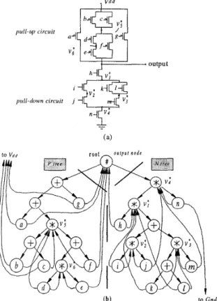
p i / / - t p c i i - u i t 4 dal V ; e-1 output h i 1,' to Vdd r o o t
-
o u r p u t n o d e ( b ) to GndFig. 3: A series-parallel circuit and its corresponding MTB tree.
6.
RESULTS
This method has been tested extensively
for
basic modules such as counters, decoders, adders, and ALU's. The CPU time comparisons are summarized in Table 1.An one-cluster circuit, also using the circuit as shown in Fig. 3(a) as an example, is simulated by using SPICE and our timing simulator BTS. The results are compared as shown in Fig. 4. The bold solid lines are the results obtained from our simulator. Five input patterns are applied to this circuit, which are case 1: (/,O,O,O,l,l,l), case 2: (l,O,O,O,/,l,l), case 3: (l,O,O,O,l,/,l), case4: (l,l,O,O,l,l,/), andcase5: (l,l,/,O,l,/ ,l), and the associated output waveforms are labeled A, B, C, D and
E,
respectively. Note that '/' represents the ramp input signal with the rising time Ins from LOW to HIGH. The waveformE
is extracted independently for its different slope, and compared with the waveform C to distinguish its difference. There are small errors presented in the simula- tion results because the target circuit is simply an one-stage circuit. 74138 7483 743817. SUMMARY
88 0.33 102.22 0.0032 11 258 0.99 774.64 0.0013 13 584 1.10 1670.98 0.00066 14An accurate waveform approximation technique is proposed, which is achieved by the new approach of delay estimation and the modified slope estimation. The new approach of de- lay estimation improves the previous version of BTS that converted the overshoot effect to the turn-on-time of MOSt (the value of VT was shifted to 3.1V), and can offer a better adaptability for a wide range of circuit and input specifica- tion. For each different fabrication process, the equations for delay estimation are derived only once. The deriving proce- dure is a simple and quick work because it can be achieved only by a few samples. Of course, this procedure can also be aided by a program on computer. The modified slope esti- mation also increases the accuracy of the transient waveform prediction, including under some special circumstances.
Circuit MOS (DX4- loo), secs ratio input event no. complex gate 2.53 0.043
(P .
inverter chain 200 0.28 241.18 0.0012
(100sta es)
Table 1: Comparisons between BTS and Spice
1 2 3 4 5 6 7 8 9 10
time, ns
Fig. 4: The simulated waveforms of the circuit as shown in Fig. 3(a). Bold line: BTS. Light line: SPICE
8. REFERENCES
[
11 R . E. Bryant, "A Switch level model and simulator for MOS digital systems," IEEE Computers, vol. C-33, pp. 160-177, 1984. [2] C. J. Terman, "RSIM - A Logic-Level Timing Simulator," Pro- ceedings of the IEEE International Conference on Computer De- sign, New York, pp. 437-440, November, 1983.[3] J. Rubinstein, P. Penfield, and M. A. Horowitz, "Signal delay in RC tree networks," IEEE Trans. on Computer-Aided Design, [4] T. M. Lin, and C. A. Mead, "Signal delay in general RC net- works," IEEE Trans. on Computer-Aided Design, vol. CAD-3, No.4, [5] Molin Chang, S,-J Yih and Wu-Shiung Feng, "Algorithm based on modified threaded binary tree for estimating delay affected by internal charges in CMOS gates", Electronics Letters, Vol. 32, No.
20, pp. 1877- 1879,26th September 1996.
[6] Molin Chang, S,-J Yih and Wu-Shiung Feng, "Recursive algo- rithm for calculating effective resistances in RC tree", Electronics Letters, Vol. 33, No. 2, pp. 131-133, 16th January 1997.
[7] J. H. Wang, Molin Chang, and W. S . Feng, "Binary-tree timing simulation with consideration of internal charges". IEE Proceed- ings-E, vol. 140, No.4, pp. 211-219, July 1993.
[SI F.C.Chang, C.F.Chen, and P.Subramaniam, "An accurate and efficient gate level delay calculator for MOS circuits," Proceedings of 25th ACM/IEEE conference on Design automation, Ana heim, CA, USA, pp.282-287,1988.
V O ~ . CAD-2, NO. 3, pp.202-211, 1983.
pp.331-349, 1984.