2418 IEEE TRANSACTIONS ON MAGNETICS, VOL. 47, NO. 10, OCTOBER 2011
Concentration of Magnetic Beads Utilizing Light-Induced
Electro-Osmosis Flow
Shih-Mo Yang , Punde Tushar Harishchandra , Tung-Ming Yu , Ming-Huei Liu , Long Hsu , and
Cheng-Hsien Liu
Department of Electrophysics, National Chiao Tung University, Hsinchu 30010, Taiwan
Institute of NanoEngineering and MicroSystems, National Tsing Hua University, Hsinchu 30010, Taiwan SINONAR Company, Hsinchu 300, Taiwan
Department of Power Mechanical Engineering, National Tsing Hua University, Hsinchu 30010, Taiwan
Magnetic beads are widely utilized for separating biomolecules, DNA and RNA. Traditionally, bulk magnet is utilized for manipula-tion these particles but when it comes to microscale bulk magnet is not the efficient method. Here, we utilize an organic photoconductive material, TiOPc, to generate light-induced electro-osmosis flow on chip. The fabrication process is convenient to be handled by the re-searchers and biologists without cleanroom IC fabrication facility. When specifically designed light pattern is projected onto the TiOPc substrate, the conductivity of the organic material layer within the illuminating region increases and the charges are locally assembled on its surface to form a virtual electrode. With an external ac voltage of 5 Vpp at 10 kHz, numerous magnetic beads are attracted from the nonilluminating region toward the center of light-pattern illuminating region. Driven by the moving light image, the grouped magnetic beads can be manipulated and merged in a desired way or direction. The light manipulation process provides a flexible and convenient approach for in vitro control of magnetic beads. We expect that this light-driven technology would display a multifunctional platform for manipulation of microparticles.
Index Terms—Electro-osmosis flow, light-induced dielectrophoresis, magnetic beads, TiOPc.
I. INTRODUCTION
M
AGNETIC separation technology utilizing magneticbeads, , is a rapid and convenient approach for sensitive and reliable capture of specific proteins, genetic ma-terial, and other biomolecules. By modifying the bead surface with the appropriate antibodies, specific target molecules such as DNA, RNA, and particular proteins are able to be adhered and separated. This approach of manipulating the microparti-cles by utilizing magnetic force exhibits less mechanical stress on the sample [1]. For lab-on-a-chip devices, electromagnets are also developed to mobilize or influence target microparti-cles via a magnetic field gradient [2], [3]. Nevertheless, a strong current applied to generate magnetic force would result in a large amount of heat thus damaging the target cells, molecules, or sample within the microsized device [4]. For microparticle manipulation, optical tweezers and dielectrophoresis force are two different separation methods based on optical and electric field, respectively. The former is applied especially between different reflective index of the microparticle and the sur-rounding. The latter is able to attract or repel the microparticle by the distortion in electric field. However, the requirement of high N.A. lens limits the working distance of optical tweezers. The nonuniform electric field generated by fixed metal elec-trodes patterned on glass substrate restricts the flexibility of microparticle manipulation. Therefore, the optoelectronic
Manuscript received February 19, 2011; revised April 25, 2011; accepted May 23, 2011. Date of current version September 23, 2011. Corresponding au-thor: C.-H. Liu (e-mail: liuch@pme.nthu.edu.tw).
Color versions of one or more of the figures in this paper are available online at http://ieeexplore.ieee.org.
Digital Object Identifier 10.1109/TMAG.2011.2158194
tweezers (OET) which possess the features of light-induced method and nonuniform electric field was introduced in 2005 [5]. A simplest design of OET chip is fabricated by using the photoconductive material, amorphous silicon(a-Si). When light image is projected on a-Si layer, the conductivity of a-Si within the illuminating region increases and the charges would trans-port photoconductive layer. The virtual electrode formed on the surface enables microparticle manipulation via dynamic light pattern [5], [6]. Besides this, another approach of microparticle concentration via light-induced electro-osmosis flow has been published [7], [8]. The potential of light-driven approach is its flexibility of microparticles manipulation, especially in biomedicine and lab-on-a-chip. However, for biologist it is not easy to fabricate Si-based chip without MEMS background.
Our research group took efforts to reduce the burden of com-plicated fabrication process and invented an easy method for fabricating a chip. We utilized organic photoconductive mate-rial, Y-type TiOPc, to fabricate the light-induced electro-os-mosis flow (LEOF) chip which is created with a desired region of minimum liquid flow velocity for the trapping and collec-tion of magnetic beads [9]. In this paper, we integrate the op-toelectronic approach of TiOPc-based substrate and the LEOF phenomenon to manipulate magnetic beads. The approach of light-induced dielectrophoresis is different from the traditional approach utilizing magnet to attract the magnetic beads. The single and simple fabrication process does not involve processes like plasma-enhanced chemical vapor deposition (PECVD) or ion implantation. The illuminating light power utilized to induce electro-osmosis flow on TiOPc is less than the laser power [9]. This approach utilizing low-frequency region, kHz, for manip-ulating magnetic beads widens the scope of TiOPc-based opto-electronic dielectrophoresis chip. It is capable of high-efficiency concentration and enrichment of magnetic microparticles.
YANG et al.: CONCENTRATION OF MAGNETIC BEADS UTILIZING LIGHT-INDUCED ELECTRO-OSMOSIS FLOW 2419
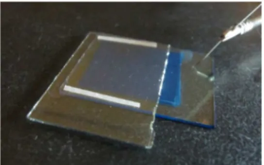
Fig. 1. TiOPc-based LEOF chip. A thin TiOPc layer, blue color, is fabricated on ITO glass substrate with a simple fabrication process.
II. CHIPFABRICATION, SYSTEM ANDTHEORY
1) Chip Fabrication: The development of OET provides a
very convenient and flexible approach for microparticle manip-ulation. The usual OET chip fabrication requires several specific cleanroom fabrication processes and facilities which are not easily accessible for biological researchers [5]. The a-Si layer is fabricated on the thin Al layer by the PECVD process [5], [6]. In 2009, Lee et al. reported another OET device by using bulk-heterojunction polymer. However, the fabrication and op-eration process should be carried out in nitrogen glove box in order to avoid the polymer material to be decayed by water and oxygen [10]. In 2010, Wu et al. reported another design utilizing boron implantation, reactive ion etching and dielectric filling to fabricate their new OET chip [11]. It was used to ma-nipulate cells in culture medium of high ion concentration, but five micro fabrication steps were required to fabricate the chip. Since the targeted applications of OET are for biological pur-pose, the complicated microfabrication processes limit the re-searchers without IC or MEMS background. In this paper, we designed the TiOPc-based LEOF by using simple fabrication process. This material is an electrophotography sensitive and absorbs light from visible to IR region [9]. A drop of TiOPc so-lution is spin-coated onto the 4 cm 3 cm ITO glass substrate with the spin speed of 1500 r/min, and then hot baked at 120 for 30 min. Then, a thin TiOPc layer of 500 nm is obtained on the ITO surface. The material property of TiOPc coated on the ITO glass remains stable for months under normal operation, which is to avoid electrolytic-bobble generation in the low ac frequency and high voltage. Finally, an ITO glass is placed on the TiOPc substrate with a 100 gap between them to obtain the TiOPc-based LEOF chip. The gap distance is defined via the number of layers of double-sided tape. The ease in fabrication process of the chip makes it available whenever necessary. The prototype chip is shown in Fig. 1.
2) Optical System: The optical system of TiOPc-based
LEOF chip is illustrated in Fig. 2. The light source (Philips UHP mercury lamp) is concentrated as a straight beam through a pair of focusing lenses and illuminated on the digital mi-cromirror display (DMD). The reflecting image is projected on the TiOPc surface of LEOF chip through a 1/20X optical system which consists of two lenses of 10 and 200 mm focal length. The dynamic image is controlled by controlling the DMD surface in real time. An XYZ translation stage is utilized
Fig. 2. Optical system setup for on-chip manipulation of magnetic beads by LEOF.
for tuning the chip position and a function generator is used to provide external ac voltage. The microparticle manipulation process is recorded by a CCD.
3) Electro-Osmosis Flow: For general microparticle
manip-ulation via light-induced OET, dielectrophoresis (DEP) force dominates at cellular scale. For example, on the TiOPc-based chip the cell with 10 diameter can be driven by the DEP force of about 5 pN. The force acting on a spherical particle of radius suspended in a medium with relative permittivity is given as [12]
where is the root mean square of the ac electric field and is the Clausius--Mossotti (CM) factor which depends upon the applied angular frequency and the electrical conduc-tivities of the particle and the medium:
According to the dielectrophoresis principle, the force is pro-portional to the third power of the particle radius. It means that the DEP force acting on magnetic beads of 1 diameter is 1/1000 times compared to the force of cell manipulation [9]. The force available is too small to drive the magnetic beads. There-fore, another phenomenon, electro-osmosis flow, should be con-sidered especially in the presence of low applied frequency.
When external ac voltage is applied to LEOF chip, free cations in the electrolyte are strongly attracted toward the illuminated TiOPc surface. This immobile charge layer is named as the compact layer with the thickness of about several angstroms. Because of this electrostatic charge attraction, the cation concentration near the TiOPc surface is higher than that in the bulk fluid. The region from the compact layer to the uni-form bulk liquid is named as the diffuse layer. The diffuse layer (mobile ions) and the compact layer are called the electrical double layer (EDL). When a tangential electric field component is applied in the EDL region, the ions in this region get driven. The velocity of these ions is called the slip velocity, ,
2420 IEEE TRANSACTIONS ON MAGNETICS, VOL. 47, NO. 10, OCTOBER 2011
Fig. 3. Schematic diagram of TiOPc-based LEOF chip utilized for concentra-tion of magnetic beads. The charges transport through the organic photoconduc-tive material layer within illuminating region and induce LEOF on the surface. The induced liquid flows at the edge of illuminating area concentrate the mag-netic beads toward the center of light pattern. Microparticle concentration is increased via dynamic light pattern.
which is defined by the Helmholtz–Smoluchowski equation [7], [8]
where is the Debye length, is the charge per unit area of induced charge of the double layer, is the tangential com-ponent of the electric field, and is the bulk liquid viscosity. When the surrounding liquid is homotypic with the same Debye length, surface charge density, and liquid viscosity, the EOF ve-locity can be rewritten as
Due to the aforementioned relationship, a nonuniform elec-tric field can generate the corresponding liquid flow. When light image is projected on the TiOPc layer, the electric field near the image edge is nonuniform. The light-induced electro-osmosis flow could be utilized to concentrate the microparticles, mag-netic beads.
III. EXPERIMENTALRESULTS
1) TiOPc-Based Chip Operation: Concentration of magnetic
beads on TiOPc chip is illustrated in Fig. 3. When light pattern is projected on the TiOPc layer, the conductivity of TiOPc in the illuminating region increases. When ac voltage is applied to the chip, the charges at the illuminating region are transported and assembled to form a virtual electrode on the TiOPc surface. The top ITO glass and the bottom virtual electrode generate a nonuniform electric field across the buffer. The maximum tan-gential electric field is formed near the edge of light image. The charges near the edge of the illuminating region are driven and then the liquid near the surface is pumped with the mobile charges simultaneously. The arrows in Fig. 3 illustrate the di-rection of the driven flow. When the ac voltage of 5 Vpp at 1 kHz is applied, the nonuniform electric field induces the charge moving of the electric double layer to pump the liquid slip ve-locity. The 2 diameter magnetic beads are then concentrated and assembled toward the illuminating region.
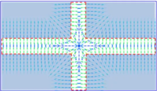
Fig. 4. Flow direction simulation of the light-induced EOF. The region within red dotted line is the projected light pattern. The arrows indicate the liquid flow direction on the TiOPc surface. The center of the pattern cross has the minimum liquid flow to trap magnetic beads.
2) Synthesis of Electro-Osmosis Flow: To verify the
EOF effect induced by the electric field gradients above the TiOPc virtual electrode, a commercial finite element software CFD-ACE+ (CFDRC, Huntsville, AL) is utilized to simulate the light-induced flow as shown in Figs. 4 and 5.
Because the conductivity of the TiOPc layer within illumi-nating region is increased, the charges transport to this photo-conductive layer and form the virtual electrode. The maximum nonuniform electric field is at the edge of the light pattern which drives the liquid slip in this region. In Fig. 4, the blue/green ar-rows indicate the flow direction. The minimum flow velocity re-gion is at the center where the light pattern crosses. Thus, taking the advantage of the region with minimum flow velocity, we trapped the magnetic beads in this region. Moving the center of light pattern is equal to moving the magnetic beads. Fig. 5 sim-ulates the flow velocity and shows the region of minimum flow velocity appearing at the center, which traps the magnetic beads.
3) Concentration of Magnetic Beads: Magnetic
microparti-cles coated with antibodies on its surface are able to adhere or trap targeted microparticles such as cell, DNA, or biomolecule for separation and sorting purpose [2]. In this study, we applied light-induced electro-osmosis flow to concentrate magnetic beads in order to widen the scope of TiOPc-based optoelec-tronic chip. The concentration process includes two steps. First, the magnetic beads are attracted from the nonilluminating region to the light pattern region due to the light-induced electro-osmosis flow. The applied ac voltage generates large flow velocity; thus, the applied voltage is tuned below 10 Vpp. When the applied ac voltage is minimized, it is very important to avoid the generation of electrolytic bubbles because the bubbles generated on the ITO glass would damage the TiOPc layer. Second, two groups of magnetic beads are combined together by moving the cross light image. When we move the light image bar, the magnetic beads trapped within the crossed center of light pattern can be manipulated and merged. Fig. 6 demonstrates the concentration process of magnetic beads. When the cross moves downward, the trapped magnetic beads at the cross center region are also driven. When two cross light patterns are merged, the two groups of magnetic beads are combined together as shown in Fig. 6(a)–(d). By these manipulations, the spreading magnetic beads are collected and concentrated. The results demonstrate that our LEOF approach has better flexibility than the traditional approach.
YANG et al.: CONCENTRATION OF MAGNETIC BEADS UTILIZING LIGHT-INDUCED ELECTRO-OSMOSIS FLOW 2421
Fig. 5. Simulation results of flow magnitude of the light-induced electro-osmosis flow. (A) Height represents the magnitude of the flow. The maximum slip velocity is at the edge of the light pattern. This liquid flow is utilized to drive the magnetic beads toward the illuminating region. (B) Minimum flow velocity is at the center where the light pattern crosses wherein the magnetic beads are trapped.
Fig. 6. Large numbers of magnetic beads are concentrated by the light-induced EOF at applied voltage of 5 Vpp, 10 kHz. (A)–(D) Two groups of magnetic beads are merged by moving the light pattern. When the light bar is moved downward, the light-induced liquid flow would drive the magnetic beads and keep their position within the center of light pattern.
Fig. 7. Single magnetic bead is driven toward the center of the light pattern. At 10 kHz and 5 Vpp, the liquid is driven at the edge of the light pattern. As a simulation of Fig. 2, the magnetic bead indicated by a red arrow within the light pattern is attracted to the minimum flow velocity region.
Single magnetic bead driving and collection by light-induced EOF is shown in Fig. 7. At applied ac voltage of 5 Vpp, 10 kHz, the liquid flow is generated to drive the magnetic bead indicated with a red arrow along the center of light pattern. It is attracted at the light pattern center which is the region with minimum flow velocity.
IV. CONCLUSION
We demonstrate the optoelectronic concentration of magnetic beads and its manipulation on organic photoconductive mate-rial, TiOPc, substrate. This paper reports a convenient and flex-ible approach for magnetic beads’ concentration on chip. Under 5 Vpp and 10 kHz conditions, the nonuniform electric field induced via virtual electrodes on TiOPc surface would gen-erate slip flow to drive the magnetic beads. This light-induced electro-osmosis method benefits the efficiency of concentration and purification for small molecules such as DNA, RNA, and proteins.
ACKNOWLEDGMENT
This research was financially sponsored by National Science Council (Grant No.98-2120-M-007-003). The authors would like to thank Prof. H.-Y. Chang from the Institute of Molec-ular Medicine, National Tsing Hua University. They also wantk to thank Prof. M. C. Wu at University of California, Berkeley, Prof. P.-Y. Chiou at University of California, Los Angeles, and Prof. G.-B. Lee at National Tsing Hua University for helpful discussions.
REFERENCES
[1] Z. M. Saiyed, S. D. Telang, and C. N. Ramchand, BioMagnet. Res.
Technol., vol. 1, p. 2, 2003.
[2] S. H. Song, H. L. Lee, H. M. Yoo, and H. I. Jung, Sens. Actuat. B:
Chem., vol. 141, no. 1, pp. 210–216, 2009.
[3] Q. Ramadan, V. Samper, D. Poenar, and Y. Chen, J. Magnet. Magn.
Mater., vol. 281, no. 2–3, pp. 150–172, 2004.
[4] H. H. J. M. Janssen, E. J. W. ter Maten, and D. van Houwelingen, IEEE
Trans. Magn., vol. 30, no. 5, pp. 3331–3334, Sep. 1994.
[5] P. Y. Chiou, A. T. Ohta, and M. C. Wu, Nature, vol. 436, pp. 370–372, 2005.
[6] A. T. Ohta, M. Garcia, J. K. Valley, L. Banie, H. Y. Hsu, A. Jamshidi, S. L. Neale, T. Lue, and M. C. Wu, Lab Chip, vol. 10, no. 23, pp. 3213–3217, 2010.
[7] P. Y. Chiou, A. T. Ohta, A. Jamshidi, H. Y. Hsu, and M. C. Wu, J.
Microelectromech. Syst., vol. 17, no. 3, pp. 525–531, 2008.
[8] A. Jamshidi, S. L. Neale, K. Yu, P. J. Pauzauskie, P. J. Schuck, J. K. Valley, H. Y. Hsu, A. T. Ohta, and M. C. Wu, Nano Lett., vol. 9, no. 8, p. 2921, 2009.
[9] S. M. Yang, T. M. Yu, H. P. Huang, M. Y. Ku, L. Hsu, and C. H. Liu,
Opt. Lett., vol. 35, no. 12, p. 1959, 2010.
[10] W. Wang, Y. H. Lin, R. S. Guan, T. C. Wen, T. F. Guo, and G. B. Lee,
Opt. Exp., vol. 17, no. 20, pp. 17603–17613, 2009.
[11] H. Y. Hsu, A. T. Ohta, P. Y. Chiou, A. Jamshidi, S. L. Neale, and M. C. Wu, Lab Chip, vol. 10, pp. 165–172, 2010.
[12] C. T. Ho, R. Z. Lin, W. Y. Chang, H. Y. Chang, and C. H. Liu, Lab