國立交通大學
電子工程學系 電子研究所碩士班
碩 士 論 文
生醫元件可程式前端放大器
AN 8-CHANNEL LOW NOISE FRONT-END
CIRCUIT FOR NEURAL RECODING SYSTEMS
研究生 : 蔡宗昀
指導教授 : 吳重雨 教授
生醫元件低雜訊前端放大器
學生: 蔡宗昀
指導教授: 吳重雨 教授
國立交通大學 電子工程學系電子研究所碩士班
Abstract (Chinese)
1887 年,英國科學家 Augustus Waller 第一次向世人發表了心電圖。1912 年, 俄國生理學者 Vladimir Vladimirovich Pravdich-Neminsky 紀錄下腦部的電波訊號。 而十九世紀末科學家也紀錄到了肌肉裡的電訊號。自從這些生理訊號一一被發現 後,人類發現這些訊號和許多神經上的疾病或身體上的活動息息相關。所以深入 的研究這些生理訊號變成了重要的課題。 由於生理訊號有低頻、低振幅且獨特等特性,所以訊號的放大、低雜訊且有 可 調 性 成 為 訊 號 處 理 的 一 大 挑 戰 。 本 論 文 即 為 實 現 一 個 可 以 用 於 放 大 Electrocochleography(ECoG)、Electromyography(EMG)和 Electrocardiography(ECG) 等多種生理訊號的類比前端放大器,且為了能夠同時觀察多個通道,本設計使用 八通道架構,此類比前端放大器包含了前級放大器,八通道多工器和可程式增益 放大器。其中新架構的前級放大器可防止電極造成的直流電壓偏移飽和電路,高 頻截止頻率可調於 1Hz-7KHz,放大增益 40 dB,輸入參考雜訊電壓在 0.5 Hz 到 7 KHz 積分範圍為 0.9 μVrms,雜訊效率因子(NEF)為 1.3。 整體的類比前端放大器的放大增益為 40-74.1dB,輸入雜訊在 0.5 Hz-7 KHz 頻段積分為 5.1 μV rms,並且有很高的共模拒斥比和電源拒斥比,功率消耗 446μW,在台灣積體電路製造股份有限公司與國家晶片系統中心的幫助下,此類 比前端電路晶片將以 0.18 微米製程實現。An 8-Channel Low Noise Front-End Circuit for
Neural Recoding Systems
Student: Tzung Yun Tsai
Advisor: Prof.
Chung-Yu Wu
Department of Electronics Engineering & Institute of Electronics
National Chiao-Tung University
Abstract (English)
This paper presents an 8-channel analog front-end (AFEA) circuit for neural recording systems. An eight-channel chopper stabilized pre-amplifier, an 8-to-1 analog multiplexer, and a programmable gain amplifier are designed. It is designed for amplification of different kinds of biopotential signals, such as electrocorticogram (ECoG), electrocardiogram (ECG) and electromyogram (EMG). These biopotential signals have the characteristics of small amplitudes, low frequency and variability. The maximum gain of AFEA is 74.1dB. The high-pass corner can achieve as low as 0.8Hz and low-pass corner can be adjusted to several kilohertz to suit for different kinds of biosignals. It is fabricated in TSMC 0.18 μm CMOS process and achieves an input-referred noise of 5.1 μVrms (input referred noise of pre-amplifier is only 0.9μVrms), bandwidth up to 7 KHz while only consumes 446 μW at 1.8V power supply. And the noise efficiency factor (NEF) is only 1.3 for pre-amplifier.
Acknowledgements
感謝 這本論文獻給我逝去的青春,沒有這三年的犧牲就沒有這本論文。 要感謝的人太多了,這不是僅僅謝天就能解決的,首先要謝謝我的指導教授 吳重雨教授,在這期間因為老師身為學校的大家長,不但要繁忙於校務,還要抽 空來指導我們學術研究,這些日子以來,讓我獲益匪淺。再者也要謝謝 CY group 的學姊長,有他們的指導,我才能在經過一千一百多個日子後終於畢業了!超感 動的啦!感謝文嘉學長、烜毅學長、夙勇哥還有仿生中心的丘丘學長,在課業上 給我很多指導,還有邱主任的志瑋學長、冠州學長在量測上和界儀器上給了我很 多方便。然後要感謝實驗室歡樂的學長姊、學弟妹和一起共甘苦的同學們!(點 名嚕!!!):跟每一屆都很熟的洨州哥、很瘦但是看起來其實很壯的甜食北鴨、 美食達人阿邦哥、戰隊 leader & 玩樂勸拜組長 professor (又名小凡)、消失很 久的變胖的台積宅、周年慶一定會出現的建名、看到就會心情很好的大正妹佳琪、 超機動看起來很歡樂的筱妊、不要再叫我學長的宗恩、世範,歐陽,紹岐、萬諶、 大仔、科科、區文…等學長姐們(註解打太累了= =)。歡樂嘴砲ㄎ group 三人組 林良(還有在 CS 上調戲妹嗎?)、溫董(超壯型男 JJ)、哲綸(吼~~~你真的很可愛)、 好想偷捏你小 BABE 的人妻怡歆、天然呆但都書卷的惠雯、兼顧歡樂與學業理 性與感性事業情場兩得意的天哥、看起來很大支而且很霸氣卻超迷 SNSD 的 Kitty 、棒球很強會玩桌遊的彥緯、很想變壯並且想脫團很久(兩件事是兩碼子事情) 的邱神、冷面笑匠超低調余降拳(吼~~~都不介紹你女友給大家認識認識)、即時 戰略達人昕爺、股票達人小賴、SNSD 三人組之一天勾 ADAIR、超強學習能力 超好但是喜歡 SNSD 的黑熊。還有眾家學弟們:嘴砲而且超宅的明翰哥、超辣每 天衣服穿不一樣的小飛機、做事很認真老師都看不到的的子薰= =、人生勝利組的阿亮、志偉、元復、YOYO、安仔還有我們的大師姊超可愛的麗珍,很想聽你 們合唱狗男女的二人組小狗達、痴痴、還有其他學弟們…好多人寫得好累(其他 學弟妹不好意思啦 XD)。對了還沒寫完,那還要謝謝這麼多年還跟我很麻吉的朋 友們朱哥、小豆、洪 R、于翔、冷峰、佳智、水蛭毛、樺樺、千華、胖子、宇翔、 Z0、岳庭育庭&小貝…等等族繁不及備載,還有要特別感謝小南,在碩班的日子 陪伴著我,謝謝你讓我在這苦悶的研究生涯增添了許多色彩。最後要謝謝我的爸 媽還有哥哥和大嫂,我愛你們,謝謝你們(我好像在做得獎感言)。 蔡宗昀 謹 致 於 交大竹塹 庚寅冬
Contents
Abstract (Chinese) ... i Abstract (English) ... ii Acknowledgements ... ii Contents ... iv Figure Captions ... v Table Captions ... vi Chapter1 Introduction ... 1 1.1 background ... 11.2 Overview of Biopotential signals ... 2
1.3 Review on Biopotential Amplifiers ... 8
1.4 Motivation ... 14
1.5 Main Results and Thesis Organization ... 14
Chapter2 Circuit Design and Simulation Results ... 16
2.1 Target Specifications ... 17
2.2 Design Consideration ... 17
2.3 Circuit Design ... 19
2.3.1 Low Noise Pre-Amplifier Circuit ... 19
2.3.2 Analog Multiplexer ... 24
2.3.3 Programmable Gain Amplifier ... 29
2.4 Post-Simulation Results ... 35
Chapter3 Experimental Results ... 45
3.1 Chip Layout Descriptions ... 45
3.2 Measurement Setup ... 47
3.3 Measurement Results ... 50
3.4 Discussion... 54
Chapter4 Conclusions and Future Work ... 59
4.1 Conclusion ... 59
4.2 Future Work ... 60
REFERENCES ... 61
Figure Captions
Fig. 1 The architecture of rail to rail instrumentation amplifier [10] ... 9
Fig. 2 Structure of [11] ... 10
Fig. 3 Architecture of [12] ... 11
Fig. 4 The schematic of biopotential amplifier rejects DC offset [13]. ... 12
Fig. 5 An implantable epilepsy detection and stimulation system includes signal process loop, monitoring and controller, and power delivery. ... 16
Fig. 6 Structure of AFEA. ... 18
Fig. 7 Architecture of the pre-amplifier. ... 19
Fig. 8 Simulated noise power spectrum of the operational transconductance amplifier of pre-amplifier circuit. ... 20
Fig. 9 (a) schematic of pseudoresistor . (b) The diagram is the simulation results of the impedance of the pseudoresistor, when VB is connected to VDD. Blue line, red line, and green line respectively represent results in the condition of TT corner, FF corner, and SS corner. ... 21
Fig. 10 (a) Schematic of OTA used in the pre-amplifier. (b) Bias circuit. (c) common-mode feedback circuit. ... 22
Fig. 11 Schematic of adjustable passive low pass filter. ... 23
Fig. 12 Equivalent circuit model of pre-amplifier ... 24
Fig. 13 Structure of analog multiplexer. ... 25
Fig. 14 Switch of analog multiplexer consists of NMOS switch, inverter, and dummy switch. The dummy switch size is half of NMOS switch. ... 25
Fig. 15 Architecture of switch control circuit (a) 3-digital counter (b) 3-to 23 decoder (c) resettable D-flip flop... 27
Fig. 16 Schematic of differential difference amplifier (DDA) (a) with common mode feedback and bias circuit (b). ... 28
Fig. 17 According to the simulation result of Monte Carlo analysis, output offset of analog multiplexer is less than 1.5mV. ... 29
Fig. 18 (a)Schematic of PGA circuit. (b) The detail diagram of 𝐶1. ... 30
Fig. 19 Operating mode of PGA: (a) hold mode (b) sampling mode. ... 31
Fig. 20 Non-overlapping clock generation circuit. ... 32
Fig. 21 Schematic of op-amp of PGA. ... 35
Fig. 22 The diagram shows the frequency response of pre-amplifier under in TT, SS, and FF corner and the control voltage of low pass filter (VLP_ctrl) is 0.1V. ... 36
Fig. 23 Frequency response of pre-amplifier under TT corner. ... 37
Fig. 24 Simulated pre-amplifier input-referred voltage noise spectrum. ... 37
Fig. 26 FFT analysis of the analog multiplexer. ... 39
Fig. 27 The diagram shows the output waveforms under different gains as input frequency is 10-KHz and its amplitude is 20mVPP. The purple line, red line, blue line, and green line represent output of gain of 1,3,11, and 51 respectively. ... 40
Fig. 28 Output power spectrum density of PGA... 41
Fig. 29 Transient waveform of the AFEA when a 10 kHz 200 μVp-p sine wave is used. ... 42
Fig. 30 The worst case simulation: The odd input channels and even input channels provide 180 different phase signals respectively. The frequency of input signals is 10-KHz and its amplitude is 200μVPP. The diagram shows the worst case output waveform. In this case, the AFEA is set in gain of 74.1dB. ... 43
Fig. 31 Layout of AFEA. ... 46
Fig. 32 Digital signal lines (Red block) closed to analog circuit are protected by shielding metal. Green block represents the VIA though all shielding metal. ... 46
Fig. 33 Chip microphotograph. ... 48
Fig. 34 Measuring environment ... 48
Fig. 35 Instrument setup for noise analysis. ... 49
Fig. 36 Instrument setup for CMRR. ... 49
Fig. 37 Instrument setup for PSRR analysis. ... 50
Fig. 38 The frequency response of Pre-amplifier circuit for different low pass corner frequency. ... 51
Fig. 39 Spectrum results for measuring CMRR (a) input (b) output. ... 52
Fig. 40 Spectrum results for measuring PSRR (a) input (b) output. ... 52
Fig. 41 Frequency response of AFEA ... 52
Fig. 42 Input referred noise spectrum density. ... 53
Fig. 43 Simulation and measurement results about frequency response of pre-amplifier are shown above when LP_ctrl=0.1V. ... 55
Fig. 44 Measurement setup for ECG ... 56
Fig. 45 ECG waveform measured at output of chopper stabilized pre-amplifier ... 56
Fig. 46 Measurement setup for EEG (signal generated by EEG simulator) ... 57
Fig. 47 EEG waveform measured at output of chopper stabilized pre-amplifier ... 57
Table Captions
Table I The electrical characteristics and applications of these biopotential signals [3]. ... 4Table II Target specification of this work. ... 17
Table III simulated characteristics of pre-amplifier circuit. ... 38
Table IV Simulated results of analog multiplexer. ... 40
Table V Simulated results of PGA. ... 41
Table VI Summary of AFEA simulated result. ... 44
Table VII Measure Result of AFEA. ... 54
Table VIII Comparison of measurement and modified simulation results. ... 55
Chapter1
Introduction
1.1 Background
In 1887, the British physiologist Augustus Waller published the first human electrocardiogram. In 1912, Russian physiologist Vladimir Vladimirovich Pravdich-Neminsky recorded the potential of the mammalian brain and evoked potentials on photographs and coins the term „ electrocerebrogram ‟. The scientist also recorded electrical activity during a voluntary muscle contraction in late 19th century. And then scientists discover these biopotential signals and some neurological disorders or physiological activities are closely related. It‟s become an important issue to explore the meaning behind the biopotential signals. The study is about the amplifier for neural recording applications.
The circuits of recording biopotential signals have to overcome various problems, while extracting the biopotential signals from the human body. These problems are not only due to the exceedingly weak characteristics of the biopotential signals but also due to the environment and the instruments that are being used during the signal acquisition. Therefore, the design of readout circuits for the biopotential acquisition systems requires a comprehensive understanding of not only the analog circuit design techniques but also the origin and the characteristics of the biopotential signals.
This chapter gives a brief introduction to the challenges of biopotential readout circuit. Section 1.2 introduces about the characteristics of the biopotential signals, which including Electroencephalogram (EEG), electrocorticogram (ECoG), electrocardiogram (ECG) and electromyogram (EMG). Section 1.3 describes review
on fronted-end amplifiers for neural recording systems. Section 1.4 explains the motivation and specifications of this work. Section 1.5 briefly introduces about main results and thesis organization.
1.2 Overview of Biopotential signals
Biopotential signals are electric potential signals that is measured between points in living cells, tissues, and organisms, and which accompanies all biochemical processes.These cells generate an potential when they are stimulated and they present a resting potential electrically.The membrane potential of an inactive cell is called the resting potential. The potentials are generated by the exchange of ions between inside and outside cell. Intracellular concentration of potassium (K+) ions is 30-50 times higher than extracellular it. Sodium ion (Na+) concentration is 10 times higher outside the membrane than inside. In resting state, the membrane is permeable only for potassium ions. K+ concentration of the interior of the cell is much higher than the exterior. Therefore, a diffusion gradient of K+ occurs towards the exterior of the cell making the interior more negative relative to the exterior, which results in an electrical field direct inward cell being built up. In steady state, the diffusion gradient of the K+ ions is balanced by the electrical field and the equilibrium is reached with a polarization voltage of nearly −70 mV. When membrane stimulation exceeds a threshold level of about 20 mV, so called action potential occurs. Sodium (Na+) and potassium (K+) ionic permeability of the membrane is changed. Sodium ion permeability increases very rapidly, allowing sodium ions to flow from outside to inside, result in the polarity of cell being more positive. Oppositely, the more slowly increasing K+ ion permeability permits K+ ions to flow from inside to outside, thus
returning membrane potential to its resting value. As the potential reaches to 40 mV, the permeability of the membrane to Na+ ions decreases and to K+ increases, resulting in the membrane potential swiftly decrease towards its rest state. The biopotential signals, such as EEG, ECG, EMG, are the result of several action potentials produced by a combination of different cells [1].
Many organs in the human body, such as the heart, brain, and muscles, display their function through electric activity [2]. The heart, for example, produces a signal called the electrocardiogram (ECG). The brain produces a signal called an electroencephalogram (EEG) or electrocorticogram (ECoG). The activity of muscles, such as contraction and relaxation, produces an electromyogram (EMG). Measurement of these biopotential signals can help doctor to diagnose what happened with these organs. Therefore, more and more studies are about the biopotential signals readout circuit. Biopotential signals have the characteristics of small amplitude, low frequency and variability. Table I shows the frequency and amplitude characteristics of EEG, ECoG, ECG and EMG. The following articles briefly introduce about these biopotential signals individually:
Table I The electrical characteristics and applications of these biopotential signals [3].
Source Amplitude (mV) Bandwidth (Hz) Clinical and Research Use EEG 0.001-0.01 0.5-40 Seizure detection, the diagnosis
of encephalopathy
ECoG 0.1-1 0.5-40* Sleep studies, seizure detection, cortical mapping
ECG 1-5 0.05-100 Diagnosis of ischemia,
arrhythmia, conduction defects
EMG 1-10 20-2K Muscle function, neuromuscular
disease, prosthesis
*Note: In order to observe the relations between KHz signals with seizure detection, the bandwidth is extended to 7KHz in this work.
EEG & ECoG:
The brain transmit electrical signals when subject‟s intention to do some action. These signals are generated by neurons in the cortical layers. There are several
modalities to capture the electrical activities of brain in clinical practice. The methods are classified by the locations the electrodes are placed on, and by the spatial and spectral frequency of their captured signals. Electroencephalogram (EEG) is measured by electrodes are placed on scalp which is 2-3 cm away from the surface of the cortex. This is safest way to record brain activities. In contrast, electrocorticogram (ECoG) which need to use invasive electrodes is more unsafe. The recording electrodes are approximated on the cortical surface, and therefore ECoG has larger amplitude than EEG [4].
The EEG is typically described in terms of rhythmic activity and transients. By means of Fourier transform power spectrum from the raw EEG signal is derived. In power spectrum contribution of sine waves with different frequencies are visible. Although the spectrum is continuous, ranging from 0 Hz up to one half of sampling
frequency, the brain state of the individual may make certain frequencies more dominant [5].
The normal EEG wave is classified five wave groups. Delta waves arise in the frequency below 3.5 Hz. They happen in deep sleep, in children, and in serious organic brain disease. Theta waves include all the waves between 4 and 7 Hz. These occur mainly in parietal and temporal regions in children, but they also occur during mental stress in some adult, particular in feeling of disappointment and frustration. The best-known and most extensively studied rhythm of the human brain is the normal alpha rhythm. The frequency range is between 8 and 13 Hz. They are found in normal persons when they are awake in a quiet, resting state of cerebration. When the awake subject is asleep, the alpha waves disappear completely. Beta wave normally occur in the frequency range of 14 to 30 Hz, and sometime as high as 50 Hz. They can be divided into Beta I and Beta II. The frequency of about 14 to 26 Hz of they is called Beta I, affected by mental activity as alpha waves. The rest waves of Beta is Beta II, on the other hand, appear during intense activation of the central nervous system and during tension [6]. Gamma waves are patterns of brain waves in humans with a frequency >30 Hz. Recent reseach have pointed out GAMMA waves observation can help to comprehend epilepsy [7][8]
The intensities of brain waves on the surface of the brain may be as large as 10mV [6]. The amplitude of EEG measured on the scalp is only few micro-volts. The electrodes of ECoG are placed more close to cortical layer. Therefore, the amplitude is larger 100 times than EEG. It‟s important about noise issue at the level of amplitude. The noises come from physiological, environmental, and electronic sources. Physiological sources of interference are motion artifact, muscle noise, eye motion or blink artifact, and sometimes even heartbeat signals. Electrical interference arises from the usual sources: 60 Hz power lines, radio frequencies (RF), and electrically or
magnetically induced interference. Moreover, the electronic components in the amplifier also contribute noise. Good design and measuring techniques can mitigate the effects of such noise and interference. Electrode locations and names are specified by the International 10-20 system [9] for most clinical and research applications. This system ensures that the naming of electrodes is consistent across laboratories. In most clinical applications, 19 recording electrodes (plus ground and system reference) are used. A smaller number of electrodes are typically used when recording EEG from neonates. Additional electrodes can be added to the standard set-up when a clinical or research application demands increased spatial resolution for a particular area of the brain. High-density arrays (typically via cap or net) can contain up to 256 electrodes more-or-less evenly spaced around the scalp.
ECG:
Electrocardiogram (ECG) records the activities of heart by placing the electrodes on the skin. It is a noninvasive recording produced by an electrocardiographic device. In clinical applications, a lead system called 12-lead system has been used usually. Ten electrodes placed on the torso, arms, and legs are used for a 12-lead ECG. And these electrodes can be combined into a number of pairs. (For example: Left arm (LA), right arm (RA) and left leg (LL) electrodes form the pairs: LA+RA, LA+LL, RA+LL) The output from each pair is known as a lead. ECGs from these different leads help define the nature of the activity on a specific part of the heart muscle. Different types of ECGs can be referred to by the number of leads that are recorded, for example 3-lead, 5-lead or 12-lead ECGs. A 12-lead ECG is one in which 12 different electrical signals are recorded at approximately the same time and are common in research and clinical application.
the measurements be interfered with noise. An important consideration in good ECG signal acquisition is the use of high-quality electrodes. Electrodes made out of silver coated with silver chloride or of sintered Ag-AgCl material, are recommended. An electrolytic gel is used to enhance conduction between the skin and the electrode metal. Artifacts at the electrode-skin contact as well as electromagnetic interference from all sources must be minimized. Since ECG instruments are often used in critical-care environments, they must be electrically isolated for safety and protected from the high voltages generated by defibrillators. [3]
EMG
Muscle fibers generate electric activity whenever muscles are active. EMG signals are recorded by placing electrodes close to the muscle group. For example, a pair of electrodes placed on the biceps and another pair placed on the triceps can capture the EMG signals generated when these muscles contract. EMG signals recorded in this manner have been shown to give a rough indication of the force generated by the muscle group. Electrodes used for such applications should be small, securely attached and should provide recordings free of artifacts. Either silver-silver chloride or gold plated electrodes perform quite well, although inexpensive stainless steel electrodes may also suffice.
Since the frequency range of EMG signals is higher than that of ECG and EEG signals, and since the signals are of comparable or larger amplitudes, the problem of motion artifact and other interference is relatively less severe. Filtering can reduce the artifact and interference: for example, setting the bandwidth to above 20 Hz can greatly reduce the skin potentials and motion artifacts.
Recording activity directly from the muscle fibers themselves can be clinically valuable in identifying neuromuscular disorders. Therefore, invasive electrodes are needed to access the muscle fibers or the neuromuscular junction. Fine-needle
electrodes or thin stainless steel wires are inserted or implanted to obtain local recording from the fibers or neuromuscular junctions. [3]
Other biopotential acquisition systems follow similar principles of measurement. In conclusion, the most of the biopotential signals have small amplitude, low frequency, and narrow bandwidth. Therefore, a circuit compatible all classifications of biopotential signals is difficult to design. The effort is required to minimize the noise and interference by improving electrode design and placement and optimizing the amplifier circuit.
1.3 Review on Biopotential Amplifiers
It‟s necessary about a front-end biopotential amplifier for the readout system due to the slight amplitude biopotential signal. The amplifier must have two characteristics: to amplify the signal and property of low noise. Considering the portable systems and implantation of human security, the power dissipation of the circuit must be minimized for long-term biopotential signal monitoring. High common-mode rejection ratio (CMRR) and high input impedance design to reduce the effect of interference from human body at 50/60Hz. Another important issue is the differential DC offset, which is generated by electrodes, results in the saturation of the amplifier. In conclusion, design the biopotential amplifier has a lot of challenges to overcome. Recently, there are four structures of circuit apply to biopotential amplifier, and are described below.
A type of biopotential amplifiers is chopper stabilized amplifier. It uses chopper technique to cancel the dynamic offset and low frequency noise of the amplifier. The low frequency noise especially means flicker noise (i.e. 1/f noise), power spectral density of which is inversely proportional to the frequency. The operation principle of
the chopper technique is that the input signal is modulated to the chopping frequency, amplified and demodulated to the baseband. The offset and noise is modulated only once, and its frequency is shifted to the chopping frequency and its odd harmonics. These modulated offset and noise can be filtered by low pass filter. must be larger than two time than the bandwidth of the input signal to prevent aliasing. And that is limited by noise issue, too. To remove effectively the 1 noise, it should be higher than the 1 noise corner frequency (at which means the frequency thermal noise and flicker noise of a circuit contributes the same spectral density).
Fig. 1 The architecture of rail to rail instrumentation amplifier [10]
Fig. 1 shows a rail to rail instrumentation amplifier for portable EEG/ECG monitoring applications. The parallel input structure utilized PMOS and NMOS replica structures provides large input common-mode range. Furthermore, it use chopper stabilized technique to reduce noise and low frequency disturbance. To reject DC offset occurred at electrode-tissue interface, R1, R2, and C1 are used to generate a
very large time constants. For achieving the goal, the capacitors are made of off-chip device. The size of off-chip devices are usually large than integrated chip. Therefore, external component is NOT suitable for implantation. Architecture of [10] consumes large power due to replica input stage. Meanwhile, this ICs is designed for conventional EEG/ECG monitoring, them possess a narrow bandwidth (150 Hz).
Fig. 2 Structure of [11]
Another chopper stabilized technique biopotential amplifier is shown in Fig. 2. The architecture consists of a micro-power chopper amplifier and multi-loop feedbacks. Gain of whole circuit is determined by the ratio of Ci and Cfb and output buffer, gain of which is generated by ratio of resistor. It improves the issue of using external component. The high pass corner is generated by Chp and switch integrator. The overall gain is associated with low cut-off frequency. It results in the complication of the design. Although it has very low power consumption, the bandwidth of [11] is merely 180 Hz. It possesses moderated noise performance and not well enough noise efficiency factor (NEF).
Fig. 3 Architecture of [12]
Fig. 3 shows the structure of [12]. That architectures are composed of a chopper stabilized amplifier and negative feedback loop is very similar to this thesis. That case has low input referred noise and very excellent noise efficiency factor performance. Switch capacitor resistors are used to generate a 150GΩ resistance. Therefore, to let high pass corner closed to DC and provide appropriate gain, the external components are still used. Although it has very low power consumption, the bandwidth of [12] is only 100 Hz and the CMRR performance is NOT good enough.
Fig. 4 The schematic of biopotential amplifier rejects DC offset [13].
The bandwidths of biopotential signals are from the millihertz range to few kilohertz range. Therefore, to rejects DC electrode offset without influence biopotential signal is difficult challenge. Fig. 4 shows the schematic of one of biopotential amplifier design [13], it claim that can generate a tens millihertz low frequency cutoff given by 1 𝐶 . 𝐶 is set to 200fP, and is a MOS-bipolar pseudoresistor consist of transistor Ma-Md. The resistance of the
pseudoresistor can reach more than 1012 ohm when the voltage across this device is between 0.2 V. the mid-band gain of this architecture is set by 𝐶 𝐶 . And -3dB corner is approximately 𝐶 as 𝐶 , 𝐶 𝐶 . Where is the transconductance of the operational transconductance amplifier.
There are a lot of interferences when measure the biopotential signals. Environmental noise (introduce in chapter 3) is one of them. Device electronic noise is the other. It is the important issue in the topic of biopotential amplifier design, since it limits the minimum signal level that the amplifier can process. Thermal and flicker noise is common type of device electronic noise. Since electrons in a conductor move
randomly by heat, the voltage across the conductor is fluctuant. The noise is called as thermal noise. The power spectral density is
(1) Where 1 1 is the Boltzmann constant. is absolute temperature. is the resistance of the conductor. According to eq. (1) the power spectral density of thermal noise does not change by frequency. It‟s a typical white noise. The flicker noise spectral density, however, depends on the frequency. Due to many dangling bonds are formed at the interface between the gate oxide and the silicon substrate in a MOSFET, the interface rises to extra energy states. The movements of the change carriers are influenced by such energy states. The flicker noise can be modeled as a voltage source with the gate terminal, and the noise spectral density is expressed as
̅̅̅̅
, (2)
Where is a process-dependent constant on the order of 1 . 𝐶 is the gate oxide capacitance per unit area. Therefore, flicker noise is also called 1/f noise [14].
The noise level of amplifier depends on the power dissipation of circuit. To consider the tradeoff between power and noise and therefore a factor called noise efficiency factor (NEF) is first described by [15]. NEF normalize the power-noise performance and bandwidth of different circuits and can be expressed as:
√
Where is the total input referred voltage noise of the amplifier, is the total amplifier supply current, and BW is the -3dB bandwidth of the amplifier in Hertz. The NEF of a single bipolar transistor without 1/f noise is 1. Therefore, NEF is
a factor which implies the performance of the biopotential amplifier in comparison with a single bipolar transistor. In [13], the amplifier reduces the noise by using large MOS transistor size and the NEF of the circuit is down to 4.
1.4 Motivation
Some published amplifier circuit for biopotential signal applications have been reviewed and surveyed. According to the research mentioned before, an attempt to make further improvements about the noise, high PSRR and high CMRR of chip, based on proper performance and power dissipation. Furthermore, small chip area and no external component are suitable for implantation. Meanwhile, in recent study of the epilepsy monitoring, the wider bandwidth detection system is necessary for observing the relation between high frequency component of ECoG and seizure of epilepsy. Therefore, we would like to design an multi-channel analog front-end amplifier (AFEA) to achieve low noise, excellent NEF performance, wide tunable bandwidth, programmable gain, and rejecting DC offset without external components for neural recording system applications.
1.5 Main Results and Thesis Organization
An 8-channel analog front-end amplifier (AFEA) for neural recording systems is designed and fabricated. The AFEA consists of a new chopper stabilized pre-amplifier, 8-to-1 analog multiplexer (MUX), and programmable gain amplifier (PGA). The new pre-amplifier is designed with combining chopper stabilized and negative feedback with pseudoresistor to perform low noise and low frequency high
pass corner. The AFEA possess 40.3/50/60.8/74.1 (dB) four steps programmable gains. The high-pass corner can achieve as low as 0.8Hz and low-pass corner can be adjusted to several kilohertz to suit for different kinds of biosignals. AFEA achieves an input-referred noise of 5.1 μV rms, and the noise of pre-amplifier is only 0.9 μV rms, tunable bandwidth up to 10 KHz while only consumes 446 μW at 1.8V power supply. And the noise efficiency factor (NEF) is 1.3 for pre-amplifier. Meanwhile, the AFEA has more than 91dB PSRR and 105dB CMRR
The first chapter, chapter 1, introduces about the characteristics of the biopotential signals, the recent development of biopotential amplifier, the motivation and target specifications of this thesis, main results and thesis organization.
The second chapter, chapter 2, presents the flow of the circuit design includes three blocks of circuit: The new pre-amplifier combines a MOS-bipolar pseudoresistor and chopper technique. An 8-to-1 analog multiplexer and a programmable gain amplifier consists of capacitive-reset gain circuit are introduced after pre-amplifier. This chapter shows how to design them and theirs post-simulation results.
The chapter 3 of this thesis includes several parts. First, chapter 3.1 describes the consideration of the chip layout and shows the diagram of the layout. Second part introduces the measurement setup. Then, third part shows the results of measurement. The final part of chapter 3 describes the discussion of these circuits.
The last chapter, chapter 4, summarizes the major consideration of this thesis and concludes with suggestions for future investigation.
Chapter2
Circuit Design and Simulation Results
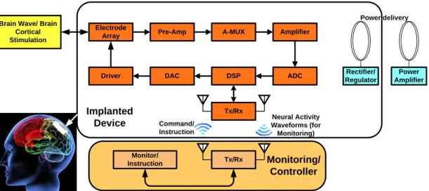
The block diagram of the implantable epilepsy detection and stimulation system can be described as shown in Fig. 5. The system includes signal process loop, monitoring and controller, and power delivery. Neural recording and stimulation loop is composed of electrode array, multi-channel pre-amplifiers, analog multiplexer (MUX), second stage amplifier (or programmable gain amplifier), analog to digital converter, DSP, Digital to analog converter, and driver for stimulation which are all implanted under skull. Monitoring and controller includes two transceivers, one is for implanted, and the other is placed outside. Power delivery supplies power to implanted device by coils. Some segments of circuits of power delivery and monitoring and controller are implanted with the loop. This thesis introduces about implementing a front-end circuit of the epilepsy detection and stimulation system. The AFEA consists of pre-amplifier, analog MUX, and programmable gain amplifier. And this chapter describes the design consideration, design flows, and post simulation results of the AFEA.
Electrode
Array Pre-Amp A-MUX Amplifier
Driver DAC DSP ADC
Tx/Rx Tx/Rx Monitor/ Instruction Rectifier/ Regulator Brain Wave/ Brain
Cortical Stimulation Power Amplifier Power delivery Neural Activity Waveforms (for Monitoring) Command/ Instruction Monitoring/ Controller Implanted Device
Fig. 5 An implantable epilepsy detection and stimulation system includes signal process loop, monitoring and controller, and power delivery.
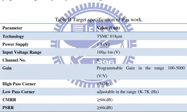
2.1 Target Specifications
Therefore, an 8-channel biopotential amplifier should be designed. This work would try to realize an 8-channel front-end circuit in TSMC 018-μm technology under 1.8V supply voltage. Its specification is listed in Table III. The constructing circuit components of the AFEA would consist a pre-amplifier, aimed at possessing high common mode rejection ratio (CMRR), low noise, DC blocking, and around 40dB mid-band gain with proper power consumption; a 8-to-1 analog multiplexer is designed to provide the 8-channel signals could be selected by next stage circuit; a programmable gain amplifier provide various gains to select.
Table II Target specification of this work.
Parameter Value (Unit) Technology TSMC 018μm Power Supply 1.8 (V)
Input Voltage Range 100μ-1m (V)
Channel No. 8
Gain Programmable Gain in the range 100-5000 (V/V)
High Pass Corner <5 (Hz)
Low Pass Corner adjustable in the range 1K-7K (Hz)
CMRR 66(dB)
PSRR 66(dB)
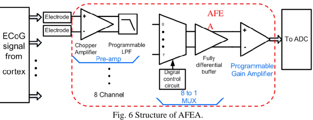
Fig. 6 Structure of AFEA.
Fig. 1 shows the main block of the circuits of this thesis. Since the system is designed for recording ECoG, the specifications of this work are made by the characteristics of ECoG. However, we make the specification of the front-end circuit flexible that let it could be appropriate for the other applications (see Table III).
Brain wave signal pass by electrode array into the pre-amplifier first stage of the AFEA. Like other biopotential amplifier as mentioned chapter 1, the brain wave like ECoG is a small amplitude signal (see Table II) and therefore the pre-amplifier must possess the characteristic of low noise, high common mode rejection ratio (CMRR), and high power supply rejection ratio (PSRR). Another reason of having high CMRR is for rejecting the DC offset voltage by differential electrodes. Hence, the pre-amplifier needs a high pass filter, too. And it also provides an adjustable high frequency cutoff. A new architecture of circuit is proposed for the pre-amplifier of the front-end circuit described in chapter 2.2.1. For practical application, the circuit needs to deal with multi-channel inputs. In this case, we choose eight-channel input to implement circuit. To reduce area and power of chip, an 8-to-1 channel analog multiplexer (MUX) is connected after pre-amplifier. The 2nd stage amplifier is composed of a Capacitive-reset gain circuit. It provides a programmable gain and stable voltage of amplified signals for ADC which follow the AFEA. These are described explicitly below.
AFE A
2.3 Circuit Design
Circuit design is divided into three parts, and a detailed description of the following three sections.
2.3.1
Low Noise Pre-Amplifier Circuit
+
- +
-C
2R
HC
1Low pass
filter
C
2R
HV
IV
OOTA
φ1 φ1 φ2 φ2=
Fig. 7 Architecture of the pre-amplifier.
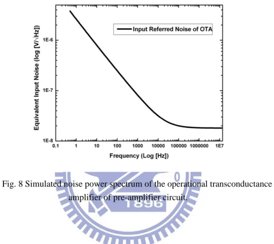
The structure of the first stage of AFEA consists of a negative feedback loop chopper stabilized amplifier with MOS-bipolar pseudoresistors and a passive low pass filter is shown in Fig. 7. As mentioned in chapter 1, the chopper stabilized technique could reduce the effect of the low frequency noise. To effectively achieve the purpose,
the chopping frequency must be larger than the 1 noise corner frequency. The 1 noise corner frequency of operational transconductance amplifier is about 60 KHz in this case (see Fig. 8). Therefore, the is chosen at 125 KHz.
Fig. 8 Simulated noise power spectrum of the operational transconductance amplifier of pre-amplifier circuit.
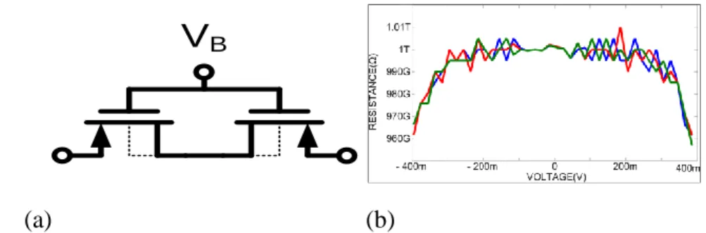
And negative feedback and high impedance MOS-bipolar pseudoresistors generate a low frequency cutoff like [16] S. Farshchi, A. Pesterev, E. Guenterberg, I. Mody, J.W. Judy; “An Embedded System Architecture for Wireless Neural Recording,”, 3rd
International IEEE/EMBS Conf. on Neural Engineering, pp. 327-332,
May 2007.] to block DC offset voltage. The are implemented using PMOS with source-and-body connected shown in Fig. 9 (a). Its impedance can reach several hundred giga-ohm in simulation (see Fig. 9 (b)). The structure of the OTA is a telescopic op-amp with embedded chopper-modulators as illustrated in Fig. 10 and similar to the design in [17]. The chopper switches are placed at low impedance nodes
to avoid affecting the bandwidth of the amplifier.
V
B(a) (b)
Fig. 9 (a) schematic of pseudoresistor . (b) The diagram is the simulation results of the impedance of the pseudoresistor, when VB is connected to VDD. Blue
line, red line, and green line respectively represent results in the condition of TT corner, FF corner, and SS corner.
OUT- Vb2 OUT+ Vb3 IN -IN+
M
1M
2M
3M
4M
5M
6M
i Vb1M
7M
8 VCMC (a)OUT+ CM Mcmc MC1 MC2 MC4MC5 MC6MC7 MC8 MC9 OUT -VCMC Vb1 (b) (c)
Fig. 10 (a) Schematic of OTA used in the pre-amplifier. (b) Bias circuit. (c) common-mode feedback circuit.
The telescopic op-amp has properties of low power, good stability, and low noise contribution [18]. Therefore, that is suitable for pre-amplifier circuit. A common mode feedback (CMFB) consists of two differential pair. The continue CMFB is more linear and could avoid the effect of chopper switch. The input referred noise of op-amp (0.1Hz to 10 KHz) is 14μV rms, the overall dc voltage gain is larger than 61dB. It has the properties of GBW more than 55MHz,phase margin > 74˚, slew rate > 25V/μs, common mode rejection ratio > 85dB, power supply rejection ratio (PSRR+) > 79dB, and PSRR- > 78dB. The op-amp of PGA dissipate 18μW.
The block next the chopper stabilized amplifier is a low pass filter. The filter is implemented by passive device shown in Fig. 11. Its function is used to filter the modulated noise and offset voltage, and therefore its cutoff frequency must be much smaller than . For the specification the system of an adjustable high low corner, a gate-voltage control variable MOS resistors and are used. The signal
transfer function of the low pass is given by
1
1 (𝐶 𝐶 𝐶 ) (𝐶 𝐶 ) Where 𝐶 includes 𝐶 and output loading of filter 𝐶 . Therefor, 𝐶 and 𝐶
are selected 2pF and 1pF respectively. VLP_Ctrl
Cf1 Cf2
Rf1 Rf2
Fig. 11 Schematic of adjustable passive low pass filter.
To simplify the analysis of the pre-amplifier, a single-ended block diagram which noise source from each device have been include in is represented as shown in Fig. 12. Where represents the noise of the OTA, and represents the noise comes from . is the open loop gain of the OTA can be written as
Where is DC gain of OTA, is the dominant pole of the OTA. The transfer function of pre-amp is then given by
𝐶 𝐶 𝐶
( 𝐶 𝐶 𝐶 𝐶 𝐶 ) 𝐶 1 𝐶
Assuming gain of OTA is approximated to in baseband. (6) can be rewritten as 𝐶 𝐶 𝐶 𝐶 𝐶 𝐶 1 𝐶
The expression shows low cutoff frequency is determined by , 𝐶 , 𝐶 , and . And mid-band gain is 𝐶 𝐶 𝐶 𝐶 which can be approximated to 𝐶 𝐶 . This stage is designed to provide a gain of 40dB, settling 𝐶 to 10pF and 𝐶
to 100fF.
+
-A(s)
sC1 sC2 GH Vi -Vo fchop fchopFig. 12 Equivalent circuit model of pre-amplifier
2.3.2
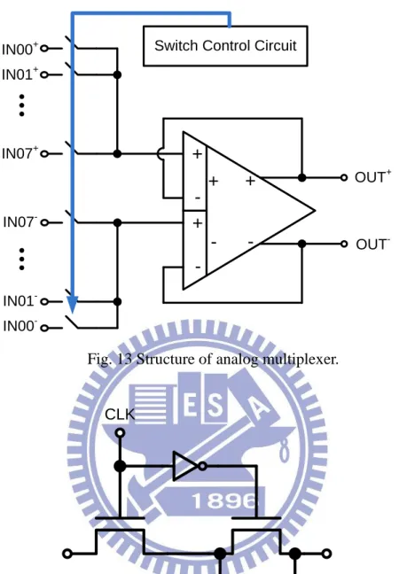
Analog Multiplexer
The analog multiplexer includes a single stage CMOS switch array, switch control circuit, and a fully differential buffer as shown in Fig. 13. There are two kind of conventional switch array, one is multi-stage switch array (i.e., switch-tree array), and the other is what we adopt. The advantage of the former is the switch control circuit is simpler than the later. However, it generates some glitch in some case. For example, when control circuit trips switches from 011 to 100, owing to the LSB change faster than the other bits, switches might change from 011 to 010, than to 000, finally to 100. Nodes of switch-tree array pre-charge to some wrong voltage. Than charge injection is produced and leads to appear the glitch at output node. This affects the accuracy of the output of the multiplexer. Single stage switch array improves the issue and applies dummy switch (see Fig. 14) to reduce the effect of charge injection.
+
-+
-+
-+
-IN00+ IN01+ IN07+ IN00 -IN01 -IN07 -OUT+ OUT-Switch Control Circuit
Fig. 13 Structure of analog multiplexer.
CLK
Fig. 14 Switch of analog multiplexer consists of NMOS switch, inverter, and dummy switch. The dummy switch size is half of NMOS switch.
Comparing with switch-tree array, the control circuit of the single stage switch array is more complicated. The switch control circuit includes 3-digital counter and 3-to 23 decoder as shown in Fig. 15. 3-digital counter is composed of three resettable D-flip flops and generate three synchronous pulses and individual frequency are 250 kHz, 125 kHz, and 62.5 kHz. The three pulses are decoded to eight 500K channel/sec switch control signals (ch00-ch07) by 3-to 23 decoder. In order to synchronize the eight switch signals, D-flip flops are place at output of decoder. It might reduce glitch
made by Asynchronous control signals.
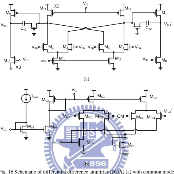
The fully differential buffer is composed of a differential difference amplifier [19] (DDA) as shown in Fig. 16. The DDA circuit results in fully balanced outputs expressed as follow
[( ) ( )]
Where is the gain of DDA. The negative feedback topology with connection between outputs and both input differential pair is utilized to produce fully differential buffer.
An important issue of this stage is offset voltage. Since the next stage, programmable gain amplifier, provide up to 50 of gain and tolerate at least 1-V output swing, the offset voltage of this stage must be much less than 8mV. Fig. 17 shows the simulation result of the offset of the fully differential buffer by using Monte Carlo analysis.
D Q _ Q D Q _ Q RESET D Q _ Q CLK 500K D0 D1 D2 (a) D2 D1 D0 CH00 CH01 CH02 CH07 D-flip flop D-flip flop D-flip flop D-flip flop (b) D Q RESET_B RESET_B φ_B φ φ φ φ φ_B φ_B φ_B Q_B (c) Fig. 15 Architecture of switch control circuit (a) 3-digital counter (b) 3-to 23 decoder
Vpp Vpn Vout -M1 M2 M11 Mi1 Vnp M3 M4 Vnn M12 Mi2 cmc Vi1 M7 M8 M9 M10 Vout+ Cc1 Cc2 Vb1 Vb1 X3 X2 (a) CM Mc6 MC1 MC2
MCi1 MCi2 MCi3 MCi4
Vout -Ibias Mb3 Mb1 Mb2 Vb1 Vi1 Mc5 cmc Vout + (b)
Fig. 16 Schematic of differential difference amplifier (DDA) (a) with common mode feedback and bias circuit (b).
700
m
800
m
900
m
1m
1.1m
1.2m
1.3m
1.4m
200
m
400
m
600
m
800
m
1m
Output Offset Voltage
Time (sec)
V
o
lt
a
g
e
(
V
)
Fig. 17 According to the simulation result of Monte Carlo analysis, output offset of analog multiplexer is less than 1.5mV.
2.3.3
Programmable Gain Amplifier
(b)
Fig. 18 (a)Schematic of PGA circuit. (b) The detail diagram of 𝐶 .
Analog to digital converter which AFEA connects to is designed in single input circuit. Therefore, the final stage of the front-end circuit would have a function of differential input to single-ended output and programmable gain. The programmable gain amplifier (PGA) circuit is realized by a single-ended capacitive-reset gain circuit as shown in Fig. 18 (a). It is based on the correlated double sampling (CDS) technique widely used to minimize errors due to reduction of offset voltage and 1/f noise. To see how this capacitive-reset gain circuit operates, consider it during the hold mode (CK2=”1”), capacitor and both stores the input offset voltage of the op-amp. At this moment, is the feedback capacitor and was charged the voltage of the output node of previous clock phase. The principle sketch is shown as Fig. 19 (a). During the sample phase (CK1=”1”) is shown in Fig. 19 (b), than becomes the feedback capacitor, and the output voltage is given by
( 𝐶 𝐶 * 𝐶 𝐶 Thus, the output voltage is independent of the op-amp offset voltage. And input signal import the circuit and the valid output voltage is generated.
+ -C1 C2 C3 + -VOS VOS + -VOUT CL + -C1 C2 + -VOS VOS +C1VIN/C2 + -VOUT =-C1VIN/C2 VIN C3 || CL (a) (b)
Fig. 19 Operating mode of PGA: (a) hold mode (b) sampling mode.
The transfer function of programmable gain amplifier in z domain is found to be [20] 𝐶 𝐶 1 1 where ( 1 1 𝐶𝐶 𝐶 ) (1 𝐶 𝐶 (𝐶 𝐶 𝐶 𝐶 )) 11 𝐶 𝐶 𝐶 𝐶 𝐶 𝐶 𝐶 1 𝐶𝐶 𝐶 𝐶 𝐶 𝐶 𝐶 1 and is the DC gain of op-amp. From the above equation, the gain of this stage is approximately the ratio of and at low frequency [21]. Therefore, two capacitor and switch arrays are used to be variable capacitors as shown in Fig. 18 (b). To match the speed of next stage, the analog to digital converter, sampling rate of programmable gain amplifier is 500 KHz the same as speed of analog multiplexer.
The design consideration of the PGA circuit is mainly focused on op-amp and switch design. In respect of switch, effect of charge injection and clock feedthrough, settling time, and linearity is generally considered about. To reduce effect of charge injection and clock feedthrough, the parasitic capacitor of switch should be minimized,
however, settling time limits size of it. Because transconductance is direct proportion to ratio of width and length, the minimum length is chosen. Fortunately the sampling rate we choose is not fast for this technology, we don‟t need to use extraordinarily large width to achieve. All switch is consist of NMOS switch except the switch connect output node to 𝐶 . A complementary analog switch is adopted in this structure due to 1-V swing output node.
The clock generation circuit used is shown in Fig. 20. It generates two phase and non-overlapping square wave. In this case, the delay time of the two phase clock signals is about 1ns.
CK1
CK2 CLK
Fig. 20 Non-overlapping clock generation circuit.
The op-amp is the primary building block of the PGA. The accuracy and speed of it are mainly determined by op-amp. During sampling mode illustrated in Fig. 19 (b), closed loop gain of PGA, AL, is expressed as
𝐶 𝐶
1
1 1 (𝐶 𝐶𝐶 𝐶 ) 1 Where 𝐶 is parasitic capacitor of input of op-amp. Let feedback factor 𝐶 𝐶 𝐶 𝐶 ), the error is represent as
1 (𝐶 𝐶 𝐶
𝐶 *
1
1 For achieving N bit resolution, error must less than 1 . Hence, the conditional expression can be got. In this case, the requirement of DC gain of the op-amp is greater than 94dB. The high gain op-amp not only reduces the gain error
but also increases the linearity.
On the other hand, the specification also limits the speed of the op-amp. By KCL equation at input node of op-amp and output node, the closed loop gain can be derived in the S domain 𝐶 𝐶 [ 1 𝐶 1 𝜏𝑎] 1 Where 𝜏𝑎 𝐶 𝐶 𝐶 𝐶 𝐶 [ 𝐶 𝐶 𝐶 ] 1 , is the transconductor of op-amp and 𝐶 is 𝐶 𝐶 . Therefore, the unity-gain bandwidth of op-amp is
𝐶 [ 𝐶 𝐶 𝐶 ] 1 The closed loop -3dB bandwidth is given by
1
𝜏𝑎 1 Then, the step response equation can be expressed as
(1 𝜏𝑎* 1
Where is the ideal output voltage (should be equal to 𝐶 𝐶 ). Let error [ ] . To ensure 1 , the condition equation could be
expressed as
𝜏𝑎 < 𝑒 𝑙𝑒
𝑁 𝑛 Where 𝑒 𝑙𝑒 is settling time, it must be much less than duty period. Using the worth case (10 bits resolution, 500 KHz sampling rate, and gain of 50) to calculate, the requirement of the unity-gain bandwidth of the op-amp is more than 54 MHz.
The op-amp must achieve high gain and large output swing (comparing to 1.8V power supply). Comparing to single stage op-amp, the two stage op-amp more meet
these requirement. Therefore, a high gain two stage configuration op-amp [22] used in PGA circuit is shown in Fig. 21. It consists of a telescopic first input stage composed of M1-M8, and common source output stage, transistor M9. This structure provides
high open loop gain and large output swing.
The dominant pole is restricted to very low frequency due to the large telescopic structure output resistance of first stage. Therefore, if using a capacitor crossing input and output of second stage to supply Miller compensation, the bandwidth would be limited. To gain more bandwidth, the CC1 capacitor provides conventional
current-buffering Miller compensation [23]. The CC2 capacitor is added to push the
dominant pole to a lower frequency effectively killing peaks of frequency response. The op-amp has GBW more than 64 MHz. The overall dc voltage gain of it is larger than 99dB. It has the properties of phase margin > 63.6˚, slew rate > 70V/μs, common mode rejection ratio > 77dB, power supply rejection ratio (PSRR+) > 80dB, and PSRR- > 95dB. The op-amp of PGA dissipates 160μW.
Fig. 21 Schematic of op-amp of PGA.
2.4 Post-Simulation Results
Post-simulation is completed by SpectrRF and HSPICE simulators with process parameters of TSMC 0.18-μm mixed signal 1P6M+ salicide 1.8V/3.3V RF SPICE models. All the simulated results are considered under TT, FF, and SS three corner and process variation. Power supply for whole analog front-end circuit is 1.8Volt. The followings are the post-simulation results of the AFEA.
☆ Pre-Amplifier Circuit
The first stage of neural system front-end circuit is the pre-amplifier. It provides 40-dB gain to amplify those biopotential signals and a low cut-off frequency
extremely close to DC. The Fig. 22 shows the frequency response of the first stage under three corners. The diagram reveals that pre-amplifier possesses a 38.8dB mid-band gain and a less than 2Hz high pass corner. The tunable low pass filter provides a high cut-off frequency with 1 kHz to 7 kHz range as shown in Fig. 23. The other important issue is about the noise. Fig. 24 is the simulated input noise power spectrum density of pre-amplifier under TT corner, and integration under this curve from 0.5 Hz to 7 kHz yields an rms noise voltage of 0.23 μV rms. noise efficiency factor (NEF) is only 0.34. The power consumption of pre-amplifier is 17.9μW. The simulation results of pre-amplifier circuit are summarized in Table IV.
Fig. 22 The diagram shows the frequency response of pre-amplifier under in TT, SS, and FF corner and the control voltage of low pass filter (VLP_ctrl) is 0.1V.
Fig. 23 Frequency response of pre-amplifier under TT corner.
Noise Floor < 30nV/sqrt(Hz)
Table III simulated characteristics of pre-amplifier circuit.
Post-simulation Parameter Value (Unit)
Gain 38.5 (dB)
fCHOP 125K (Hz)
Power Dissipation 17.95 (μW) High Pass Corner Frequency <2(Hz)
Low Pass Corner Frequency 1K~ >10K (Hz)
Input referred noise (0.5 Hz-7 kHz) 0.23(μV rms)
NEF 0.34
☆ Analog Multiplexer
The analog multiplexer is composed of switch control circuit and fully differential buffer. Fig. 25 shows the eight channel switch control signal made by the digital circuit and it provides the multiplexer 500k channel/sec switch rate to work. And a FFT analysis is shown in Fig. 26, and the total harmonic distortion is 7.278e-05% (-122.7 dB) when input frequency is 10-KHz. It would tolerate maximum 200mVPP input swing from output of pre-amplifier therefore simulated input range is
about 700mV to 1.1V is far away large than target. The power dissipation of this stage is 77.83 μW. Table V summarizes the simulated results of analog multiplexer.
Fig. 25 A simulated controlling signals in the analog multiplexer.
Table IV Simulated results of analog multiplexer.
Post-simulatiom Parameter Value(Unit)
Channel No. 8
Switching Speed 500K(Number of Channel/sec)
Power Dissipation 77.83(μW) Input Range 653~1142(mV)
THD 82.8dB (@Fin=10k)
☆ Programmable Gain Amplifier
The PGA circuit provides a tunable gain and 1-V output swing. In this case, Gain of 1/3/11/51 V/V are designed in PGA as shown in Fig. 27. The SNDR of PGA stage is greater than 62dB and SFDR is greater than 71 dB when full signal is used (see Fig. 28). The power consumption of PGA is 216 μW. The summaries of simulated results of PGA are shown in Table VI.
Fig. 27 The diagram shows the output waveforms under different gains as input frequency is 10-KHz and its amplitude is 20mVPP. The purple line, red line, blue line,
Fig. 28 Output power spectrum density of PGA.
Table V Simulated results of PGA.
Post-simulation Parameter Value (unit)
Gain 1,3,11,51 (V/V) SFDR (X1) (X51) 71.0 (dB) 72.37 SNDR (X1) (X51) 62 (dB) 63.22 THD (X1) (X51) -59.2 (dB) -64.7 (dB) fSAMPLE 500 (KHz) Bandwidth 265 (KHz) Power Dissipation 216 (μW) Output Range 1.6~0.2 (V)
Whole chip simulation results are summarized in Table VII. Programmable gain of front end circuit is 40/49.5/60.8/74.1 dB at mid-band and the cut-off frequency is less than 2 Hz. The tunable low pass filter provides the cut-off frequency of 1 kHz to 7 kHz achieved by a passive filter with tunable resistors controlled by external voltage. It is integrated from 0.5 Hz to 10 kHz to obtain rms noise voltage, whose value is 1.2 μV rms. The noise efficiency factor (NEF) of whole circuit is only 4.9. The overall power consumption is 446 μW. Whole chip simulated waveform are shown in Fig. 29 when an 10 kHz 200 μVpp sine waves as the input are used
Fig. 29 Transient waveform of the AFEA when a 10 kHz 200 μVp-p sine wave is used.
Fig. 30 The worst case simulation: The odd input channels and even input channels provide 180 different phase signals respectively. The frequency of input signals is
10-KHz and its amplitude is 200μVPP. The diagram shows the worst case output
Table VI Summary of AFEA simulated result.
Post-simulation Parameter Value (Unit)
Gain (programmable) 40/49.5/60.8/74.1dB
Low Frequency Cut-off <2 (Hz)
High Frequency Cut-off (Tunable)
1K~>10k (Hz)
Power Consumption 445.74 (μW) CMRR(@f=10K) 120(dB)
PSRR(@f=10K) 95(dB)
Input referred noise 1.11(μV rms)
Chapter3
Experimental Results
3.1 Chip Layout Descriptions
The whole chip of AFEA is fabricated in TSMC 0.18um Mixed Signal/RF process. It possesses 1 poly layer and 6 metal layers with low k inter-metal dielectric. Deep n-well topology is employed to surround the N-MOS device which allows the connection of source and body terminals to avoid body effect. MiM capacitor provides a low variation and low couple capacitor. High poly resistor, multi-Vt device and thick top metal are available for 1.8V/3.3V applications. It is suitable for logic, mixed signal, and RF designs. The layout of the front-end circuit is shown in Fig. 31. To avoid interference of digital clock to analog signal, the analog ground and power supply are separated from digital‟s. Furthermore, Digital signal lines closed to analog circuit are protected by shielding metal as illustrated in Fig. 32, and all NMOS of analog circuit are surrounded by deep n-well. With the aid of it, parasitic capacitance and noise coupling from substrate can be reduced.
The I/O pads are selected by STC Pure 1.8V Linear I/O Library in 0.18-μm CMOS Process. These I/O pads all include electro static discharge (ESD) protection circuits. Meanwhile, digital output buffer are embed in digital output pad to improve driving ability. To reduce the effect of couple of digital signals, digital I/O pads are put far away from analog ones. In this project, we select five analog observation points (outputs of pre-amplifier, outputs of analog multiplexer, and end of whole circuit.) three digital observation points (outputs of three digital counter).
1
.5
m
m
1.8mm
8-channel pre-amp
A
-M
U
X
P
G
A
Fig. 31 Layout of AFEA.
Fig. 32 Digital signal lines (Red block) closed to analog circuit are protected by shielding metal. Green block represents the VIA though all shielding metal.
3.2 Measurement Setup
This chip is directly bonded on printed circuit board (PCB). Package chip is excluded due to the reduction of more complicated parasites. And the chip microphotograph is shown in Fig. 33. On measurement consideration, we should restrict the environmental noise as possible as we can. The main environmental noise is the interference coupled from power line 50/60 Hz. Its common mode term is eliminated by front-end circuit‟s property of high CMRR and PSRR. However, other term of noise still affect the chip. The method is used to prevent that. We place a grounded connect metal plate under the PCB [24] and wrap up the sensitive line in aluminum foil. In case of long time observation, we take notice of some offset and disturbances at the output of circuit due to high impedance of pseudoresistors. To solve this issue, the control voltage of pseudoresistor (VB) occasionally down to 0V to
let the circuit “fast settle” [25]. The measuring environment and PCB of the chip are shown in Fig. 34. Fig. 35 to Fig. 37 present the instrument setup for different measuring requirement respectively.
Fig. 33 Chip microphotograph.
Agilent E4448A
Spectrum Analyzer
Fig. 35 Instrument setup for noise analysis.
HP 33120A
Function Generator
Agilent E4448A
Spectrum Analyzer
Agilent E4448A
Spectrum Analyzer
Agilent E3631A Power Supply Agilent E4448A Spectrum Analyzer HP 33120A Function Generator BIAS-TEES Agilent E4448A Spectrum Analyzer
Fig. 37 Instrument setup for PSRR analysis.
3.3 Measurement Results
The measurement results are described as following. The frequency response of pre-amplifier circuit is shown in Fig. 38. We can observe the mid-band gain of pre-amplifier is about 40dB. Meanwhile, the expected tuning range of high frequency cut-off is covered in the bandwidth of tunable low pass filter. To measure the input referred noise, input ports are shorted to ground (see Fig. 35). The spectrum that we capture at output nodes is output noise spectrum. Therefore, we can divide amplifier gain into it, and get input noise spectrum as shown in Fig.36. The noise floor is less than 1 n √ and the input referred noise integrated from 0.5Hz to 7 KHz is 0.9 μV rms.
To measure CMRR and PSRR of the front-end circuit, spectrum analyzer and signal generator are utilized to measure these specifications (see Fig. 36 and Fig. 37). The measured spectrum of common mode gain and gain from power supply are shown in Fig. 39 and Fig. 40 respectively. The AFEA possesses over 105dB CMRR
and 91dB PSRR. The power consumption of whole circuit is about 446.4 μW. The voltage is enlarged 1/3.08/10.6/51 times by PGA circuit. Fig. 41 shows the frequency response of AFEA circuit, the tunable mid-band gains of whole circuit are
40.3/49.8/60.7/74.4 (dB) respectively. The input noise power spectrum density is
shown in Fig. 42. The summary of measurement results are list in Table VIII.
Fig. 38 The frequency response of Pre-amplifier circuit for different low pass corner frequency.
(a) (b)
Fig. 39 Spectrum results for measuring CMRR (a) input (b) output.
(a) (b) Fig. 40 Spectrum results for measuring PSRR (a) input (b) output.
![Table I The electrical characteristics and applications of these biopotential signals [3]](https://thumb-ap.123doks.com/thumbv2/9libinfo/8610191.190675/13.892.127.766.204.438/table-i-electrical-characteristics-applications-biopotential-signals.webp)
![Fig. 4 The schematic of biopotential amplifier rejects DC offset [13].](https://thumb-ap.123doks.com/thumbv2/9libinfo/8610191.190675/21.892.280.648.112.466/fig-schematic-biopotential-amplifier-rejects-dc-offset.webp)