國立交通大學
國立交通大學
國立交通大學
國立交通大學
電子工程學系電子研究所碩士班
電子工程學系電子研究所碩士班
電子工程學系電子研究所碩士班
電子工程學系電子研究所碩士班
碩士論文
碩士論文
碩士論文
碩士論文
測試次臨界電壓的靜態隨機存取記憶體的開路
缺陷
Testing Open Defects for Subthreshold SRAM
Designs
研究生 :
陳弘昕
指導教授 : 趙家佐 博士
Testing Open Defects for Subthreshold SRAM Designs
研究生
:
陳弘昕
Student : Hung-Hsin Chen
指導教授 : 趙家佐
Advisor : Chia-Tso Chao
國立交通大學
電子工程學系電子研究所碩士班
碩士論文
A Thesis
Submitted to Department of Electronics Engineering & Institute of Electronics College of Electrical and Computer Engineering
National Chiao Tung University In Partial Fulfillment of the Requirements
for the Degree of Master
In
Electronics Engineering September 2010
Hsinchu, Taiwan, Republic of China 中華民國 九十九年九月
i
學生:陳弘昕 指導教授:趙家佐 博士
國立交通大學電子工程學系電子研究所碩士班
摘要
因應更低電壓系統的要求,有很大量的研究已經花在如何發展一個有效並且 更經濟使用次臨界電壓的靜態隨機存取記憶體設計上。然而在測試方法上,考慮 到最新發展使用次臨界電壓的靜態隨機存取記憶體設計還尚未完全被討論完。因 此,我們首先對很多使用次臨界電壓的靜態隨機存取記憶體設計分成三大類設計, 並且研究每一種分類上的設計的開路缺陷的錯誤行為模式。並且針對這些錯誤可 能會或是不會被傳統靜態隨機存取記憶體的測試方法所測到錯誤。針對於較難測 到的錯誤,我們會更進一步討論不同分類的次臨界電壓的靜態隨機存取記憶體設 計所對應的測試方法。最後,討論溫度在測試上需要怎運作。ii
Student:Hung-Hsin Chen Advisor:Dr. Chia-Tso Chao
Department of Electronics Engineering
Institute of Electronics
National Chiao Tung University
Abstract
Due to the increasing demand of an extra-low-power system, a great amount of research effort has been spent in the past to develop an effective and economic subthreshold-SRAM design. However, the test methods regarding those newly developed subthreshold-SRAM designs have not yet been fully discussed. In this paper, we first categorize the subthreshold-SRAM designs into three types, study the faulty behavior of different open defects for each type of designs, and then identify the faults which may or may not be covered by a traditional SRAM test method. For those hard-to-detect faults, we will further discuss the corresponding test method according to different each type of subthreshold-SRAM designs. At last, a discussion about the temperature at test will also be provided.
iii 這兩年在交通大學電子研究所學了很多東西,不僅僅是課業上吸收到很多知識以 外,還學會了處理事情的方法與解決問題的能力,這都要非常感謝我的指導老師, 趙家佐教授,願意給我機會學習並且時常鼓勵我,提供意見給我新的方向,也給 我很多機會去學習怎樣辦好一場重要的實驗旅遊,並且從中學到很多小細節才是 最重要的。要感謝的人太多了;首先要謝謝實驗室所有同仁,政偉學長在研究上 面大力支持我,且很有耐心的教會我很多東西。振安學長、增錦學長,也常常提 供研究上的意見並時常給予關心我。智為學長、偉勝學長教會我學會寫程式。再 來是思邦、皓宇的兩年陪伴一起抒發壓力、給予意見怎樣讓研究做更好。還有淳 仁,在我心情最低落時候,願意傾聽我的心聲與支持鼓勵。最後還有擴安一起買 實驗室家俱。也要感謝師大英語系雅萱長期給予心靈支持。另外,還有感謝我的 朋友們小強、大包、人瑋、冠儒、育光、銘輝、阿幹、小賴、小曲、丘山、小慧 等等。有你們才能讓我的研究所不會枯燥乏悶,再次謝謝身邊所有人的支持!! 2010 年 陳弘昕 撰
iv 摘要 --- i Abstract --- ii 誌謝 --- iii Contents --- iv List of Tables --- v List of Figures --- vi I. INTRODUCTION --- 1
II. CATEGORIZATION OF SUBTHRESHOLD-SRAM DESIGNS --- 4
III.TEST METHODS FOR STABILITY FAULTS --- 6
IV.ANALYSIS OF OPEN DEFECTS IN TYPE-A SUBTHRESHOLD SRAMS -- 10
V. ANALYSIS OF OPEN DEFECTS IN TYPE-B SUBTHRESHOLD SRAMS -- 17
VI.ANALYSIS OF OPEN DEFECTS IN TYPE-C SUBTHRESHOLD SRAMS -- 24
VII. IMPACT OF TEMPERATURE AT TEST --- 30
VIII.CONCLUSION --- 32
v
Table I Categorization of subthreshold-SRAM designs --- 4 Table II Faulty behavior of open defects on Type-A designs (Fig. 2, 3, 4) --- 14 Table III Effectiveness of test methods for detecting STFs in Type-A designs -- 15 Table IV Effectiveness of test methods for detecting fail-to-write gate open defects
in Type-A designs --- 16 Table V Faulty behavior of open defects on Type-B designs (Fig. 5, 6) --- 20 Table VI Effectiveness of test methods for detecting STFs in Type-B designs -- 21 Table VII Effectiveness of test methods for detecting fail-to-write gate open defects
in Type-B designs --- 21 Table VIII Impact of using different backgrounds when testing fail-to-read open
defects in Type-B designs --- 23 Table IX Faulty behavior of open defects on Type-C designs (Fig. 7, 8) --- 27 Table X Effectiveness of test methods for detecting STFs in Type-C designs -- 28 Table XI Impact of using different write voltages during LVW-HVR for Type-C designs --- 28 Table XII Impact of using different backgrounds when testing fail-to-read open
vi
Figure 1. Illustration of severe write
(a) Severe write for testing pMOS stability faults --- 9
(b) Severe write for testing nMOS stability faults --- 9
Figure 2. First Type-A subthreshold-SRAM design --- 11
Figure 3. Second Type-A subthreshold-SRAM design --- 11
Figure 4. Third Type-A subthreshold-SRAM design --- 12
Figure 5. First Type-B subthreshold-SRAM design --- 18
Figure 6. Second Type-B subthreshold-SRAM design --- 19
Figure 7. First Type-C subthreshold-SRAM design --- 25
Figure 8. Second Type-C subthreshold-SRAM design --- 26
Figure 9. (a) Cycle time versus temperature and --- 30
(b) Power consumption versus temperature for a 128x32 subthreshold-SRAM array --- 31
I.
INTRODUCTION
Lowering supply voltage is the most straightforward but effective method to reduce circuit’s overall power consumption, which is especially suitable for those portable, powerlimiting, and not-timing-critical applications such as wireless sensor systems and implanted biomedical chips. Previous works [1] [2] have shown that the most power-saving supply voltage falls around the subthreshold region for CMOS digital circuits and some subthreshold digital circuits have already been demonstrated in silicon successfully. Also, the performance degradation imposed by the subthreshold operations can be compensated by using proper parallel architecture [3] [4], which further extends the application of a subthreshold system.
In the process of developing a robust subthreshold system, operating SRAMs at a subthreshold voltage is more challenging than operating digital circuits. Under
subthreshold operations, the typical 6T SRAM design needs to face the following two major problems: (1) decrease of the static noise margin and (2) decrease of the write margin [5] [6]. It means that a 6T SRAM bit-cell operating at subthreshold region is more vulnerable to the noise and at the same time harder to write. Also, in order to increase the write margin, the size of the pass transistors in a 6T SRAM bit-cell needs to be increased, which may further jeopardize the static noise margin. Thus, for a 6T SRAM bit-cell, a proper combination of the 6 transistors’ sizes are extremely hard to obtained under subthreshold operations, especially when the local process variation of advanced process technologies may significantly change the device characteristics
and in turn break the fragile balance between the currents of the 6 transistors for read, write, and hold operations. Previous results [7] have shown that the minimum supply voltage for operating a 6T SRAM design is 0.7V based on a bulk CMOS 65nm technology [8] and a dynamic-double-gate SOI technology.
To overcome the above two problems and successfully operate a SRAM at subthreshold region, several new SRAM bit-cell designs[9] [10] [11] [12] [13] [14] [15] [16] were proposed. Tackling the week static noise margin, [9] [10] [11] [14] [15] utilized an extra read path (in addition to the original pass transistors) in their SRAM designs to isolate the cross-coupled inverters from the bit-lines during a read
operation, which can effectively avoid potential half select or deceptive read destruction. Tackling the inability to write, techniques were utilized to either strengthen the driving capability of the pass transistors or loose the hold ability of the cross-couple inverters during the write operation. To achieve the former one during a write operation, [9] specified a boosted word-line voltage to access the pass transistors and [16] designed the pass transistor in a way that its reverse short channel effect can be utilized under subthreshold operations. To achieve the later one during a write operation, [13] broke the loop of the cross-coupled inverters with additional transistors and [12][14][15] destroyed the functionality of one or both inverters by adjusting the voltage at its virtual ground and/or virtual VDD.
After a significant amount of research effort has been put into the area of developing an effective and economic subthreshold-SRAM design, however, the testing methodologies for those new subthreshold-SRAM designs have not been fully discussed in the literature yet. In this paper, we will first categorize the new
subthreshold-SRAMdesigns into three types based their design characteristics. For each type of subthreshold-SRAM designs, we will then discuss the fault models associated with open defects and identify the faults which may or may not be easily
detected by a traditional SRAM test algorithm. We will further discuss the
corresponding test methodologies for each of the above hard-to-detect faults. Finally, a short discuss about the test temperature will be provided for setting up the worst condition for testing. All the experimental results are collected from the simulation using an UMC 65nm low-leakage process technology.
II.
CATEGORIZATION OF
SUBTHRESHOLD-SRAM DESIGNS
The fault models of a subthreshold-SRAM design is associated with its bit-cell structure, and so are their test methodologies. In this section, we categorize the subthreshold designs [9] [10] [12] [13] [11] [14] [15] based on the following two criteria regarding the bit-cell structure (Q1 and Q2). The later discussion about the fault behaviors will be based on the result of this categorization.
• Q1: Is its read path different from its write path?
• Q2: Does the design use a single-ended sense amplifier?
Based on Q1 and Q2, the subthreshold-SRAM designs can be divided into Type A, B, C, and D as shown in Table I. In fact, Type D represents the bit-cell sharing the read/write paths and utilizing a differential sense amplifier, i.e., the traditional 6T SRAM design. Thus, our later discussion will focus on the fault models and test methods only for the designs in Type A, B, and C.
In order to analyze their fault models, we used a UMC 65nm low-leakage process to implement each of the above bitcell designs in a 128x32 array (128 bit-cells at a bit-line and 32 bit-cells at a word-line), including write drivers and sense amplifiers. Under the defect-free condition, we first identified the minimum required cycle time for correct read or write operations at the TT corner and 25◦C, and then defined the cycle time as 20% longer than the minimum required cycle time for each bit-cell design. On top of a defect-free design, we will later inject open defects and simulate whether the faulty design can function correctly within the defined cycle time.
III.
TEST METHODS FOR STABILITY FAULTS
A. Background of Stability Faults
A stability fault refers to a small open defect on the source/drain of the four
cross-coupled transistors, which may not fail a read or write operation under a typical operating condition but may fail under some corner conditions (such as significant IR drop, noise, or soft error). As a result, a stability fault may decrease the reliability of the SRAM but may not be easily detected by a conventional march sequence. Therefore, testing stability faults has become one of the most challenging task in current SRAM testing. Several test methods were proposed to detect the stability faults with as small resistance as possible [17] [18] [19] [20].
For traditional 6T SRAMs, the past research effort mainly focused on the stability faults located on the source/drain of the pull-up pMOS transistors (such as MT2 and
MT4 in Figure 1) and ignored the stability faults located on the pulldown nMOS
transistors (such as MT3 and MT5 in Figure 1), which can be detected relatively easily by a read operation because the bit-lines in general SRAMs are pre-charged to VDD during a read operation. If the nMOS transistors cannot successfully pull down a bit-line due to the open defects, then the pre-charged value (floating 1) will be read out, which is opposite to the expected value. On the other hand, if the pMOS transistors cannot successfully pull up the bit-line due to an open defect, then the pre-charged value (floating 1) just happens to be the expected value and hence the open defect cannot be detected.
However, for subthreshold-SRAM designs, the read path can be separated from the write path, meaning that the weak pull-down ability of nMOS transistors will not directly affect the voltage at RBL during a read operation. Therefore, the importance of detecting the stability faults on the pull-down nMOS transistors (MT2 and MT4) become more significant for subthreshold-SRAM design than that for traditional 6T SRAMs. In this paper, we will validate the effectiveness of the following test methods for detecting the stability faults located on both the pMOS and nMOS transistors of subthreshold SRAMs. These testing methods include: (1) read equivalent stress, (2) severe write, and (3) low-V-write/high-V-read.
B. Read Equivalent Stress
The idea of the read equivalent stress in the 6T SRAM design is to perform consecutive read operations to a designated bit-cell such that its word-line kept opened and its data stored by the cross-coupled inverters can be constantly attacked by the pre-charged VDD (floating 1) at bit-lines [17] [21]. However, for the
subthreshold SRAMs which utilizes a different read path from its write path (such as Type-A and Type-C), a read operation will turn on only its read word-line but not its write word-line. Such a read operation cannot attack the stored data and detect stability faults. Thus, to be able to apply read equivalent stress for Type-A and Type-C subthreshold SRAMs, specialized DFT circuit is required to turn on the write word-line and apply a floating 1 at write bit-lines during a read operation at the test mode.
C. Severe Write
The idea of severe write in the 6T SRAM design is to perform a write operation by setting BL and BLB to floating 0 and strong 0 at the test mode, instead of strong 1 (or
floating 1) and strong 0 at the normal mode (as shown in Figure 1) [20]. With such a write operation, successfully writing in data become more difficult since the floating 0 is opposite to the target value at Q or QB. As a result, if an open defect falls on the source/drain of pMOS transistors (such as MT2 and MT4) and weakens the pull-up ability of an inverter, then the severewrite operation will fail to write the correct data and hence detect the open defect. Figure 1(a) illustrates how a severe write helps to detect an open defect on the pMOS transistor MT4.
In fact, the above severe write (floating 0 and strong 0) can only detect open defects on pMOS transistors. To detect the stability faults on nMOS transistors, a severe write should set BL and BLB to floating 1 and strong 1. However, the nMOS pass
transistors (MT1 and MT6) are not suitable for passing a value 1, especially when operating at the subthreshold region (0.4V in our cases). Such a severe write cannot correctly write data even when no defect exists in the subthreshold SRAM. Therefore, in order to use a severe write to detect stability faults on nMOS transistors, we need to boost the voltage at WL by another Vt (0.8V in our case) to enhance the ability of passing a value 1 through the nMOS pass transistors during the test mode, which also requires extra DFT circuitry to realize. Figure 1(b) illustrates how this refined version of severe write can help the detection of an open defect on the
nMOS transistor MT4.
D. Low-V-Write/High-V-Read
The idea of low-V-write/high-V-read is similar to the severe write, which increases the difficulty of a write operation such that the degradation of pull-up or pull-down capability caused by an open defect may fail to write the correct data. At the same time, we also need to make sure that this difficult condition for write will not fail the design without any defect. It means that the low operating voltage for write cannot be
too far away from the normal voltage. Also, changing the operating voltage on test equipments takes a significant amount of time (around 10 micro seconds in our experience). Thus, we need to apply the low-V write to each word, change the operating voltage to normal, and then read each word. A high-V read immediately after a low-V write is not allowed due to its large overhead on test-application time.
IV.
ANALYSIS OF OPEN DEFECTS IN TYPE-A
SUBTHRESHOLD SRAMS
A. Design Overview of Type-A Subthreshold SRAMs
According to the categorization, Type-A subthreshold-SRAM designs utilize a single-ended sense amplifier for read and build an extra read path in addition to the traditional 6T SRAM, which can protect the value stored in the crosscoupled inverters during read operations and improve its read SNM to the same level as its hold SNM. Figure 2 shows the first Type-A subthreshold-SRAM design [9], where MA1 to MA6 represent the transistors in the traditional 6T SRAM and MA7 to MA10 represent the transistors in the read path. In this design, the original word-line (WL), bit-line (BL), and bitline-bar (BLB) are only used for write operations. The new read word-line (RWL) and single-ended read bit-line (RBL) are only used for read operations. During a read operation, the value stored at QB (Q bar) will determine the value at QBB (Q bar bar) through an inverter (formed by MA9, MA10, and MA7), and then determine the value at RBL. Also, the value of QBB is kept at 1 (VDD) or floating during the hold mode to reduce the leakage current of MA8 to RBL.
Figure 3 shows the second Type-A subthreshold-SRAM design [10]. Similar to [9], [10] also use four transistors (MA7 to MA10) to build an extra read path. However, its QBB is always kept at 1 during the hold mode since the MA9 in [10] is controlled by RWL instead of QB. When reading a value 0 out, QBB is pulled down through the path formed by MA7 and MA10. However, when reading a value 1 out, QBB is floating since MA9 is turned off by RWL. As a result, the pre-charged floating 1 at RBL will be read out.
Figure 4 shows the third Type-A subthreshold-SRAM design [11], which uses two transistors and one extra signal (named buffer-foot) to build the extra read path. During read, the signal buffer-foot is set to GND and hence its read mechanism is the same as [10]. It means that QBB is 0 and floating when reading 0 and 1, respectively. During hold, the signal buffer-foot is set to VDD, meaning that QBB is either 1 or floating based on the value of QB.
B. Impact of Open Defects on Type-A Subthreshold SRAMs
In the following experiments, we inject an open defect with different resistances on each terminal (gate or source/drain) of each transistor and report the minimum
resistance which can cause a failure on a read operation or a write operation for Type-A subthreshold-SRAM designs. Table II lists the minimum detectable resistance of each open defect (in Column 5) and the operation which the defect cause a failure at (in Column 4). Note that the result reported in Table II is obtained based on the first Type-A design [9] at the TT corner and 25◦C. A similar result can be obtained for the other two Type-A designs [10] [11]. In addition, once the a defect can generate a read
failure or write failure, this defect can be easily detected by a conventional SRAM march sequence. Therefore, we only need to consider the open defects with a faulty resistance less than the minimum detectable resistance.
As Table II shows, the open defects located on the original 6T bit-cell (MA1 to MA6) all fail on a write operation. The open defects located on the source/drain of the four cross-coupled transistors (MA2 to MA5) are first highlighted by a gray
background color in Table II. Those defects are classified as a stability fault in Section III. As opposite to traditional 6T super-threshold SRAMs, no stability faults on the nMOS transistors (MA3 andMA5) can be detected, but the stability faults on the pMOS transistors can be detected with a 60MΩ minimum detectable resistance for Type-A designs. This result demonstrates that detecting the stability faults on nMOS transistors is more critical than that on pMOS transistors for Type-A designs. Also, all open defects on the gate of the six transistor (MA1 to MA6) have a minimum
detectable resistance larger than 370MΩ, and hence are also relatively hard to detect. On the other hand, the open defects located on the extra read path (MA7 to MA10) all fail on a read-0 operation. Also, the open defects on both gate and source/drain of MA9 are almost undetectable even though those open defects may reduce the ability of pulling up QBB. However, the read-1 operation do not rely on MA9 to pull up RBL and hence the malfunction of MA9 can hardly fail a read operation. For MA7,MA8, and MA10, the open defects on their gate is harder to detect than those on their source/drain.
C. Effectiveness of Test Methods for Type-A Designs
In the following experiment, we attempt to reduce the minimum detectable resistance of each stability fault by applying (1) read equivalent stress (denoted as RES), (2) severe write, and (3) low-V-write/high-V-read (denoted as LVWHVR) to Type-A subthreshold-SRAM designs. Note that the read equivalent stress performed in this experiment will not stop repeating read operations until the
minimum detectable resistance can hardly be decreased, which usually takes less than 10 repeated read operations. Also, the operating voltage for write and read in low-V-write/high-V-read is 0.36V and 0.4V, respectively. Table III reports the minimum detectable resistance achieved by each test method. In Table III, the test method W+R means a simple read operation after a write operation, which will actually achieve the same minimum detectable resistance as listed in Table II.
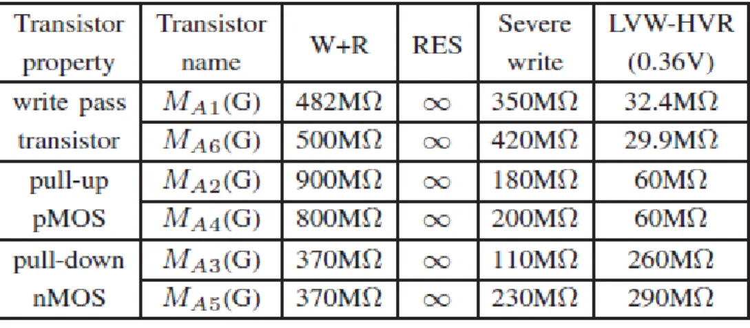
As Table III shows, severe write outperforms the other two test methods by achieving a 6.6MΩ minimum detectable resistance for pMOS stability faults and a 4.3MΩ minimum detectable resistance for nMOS stability faults. Meanwhile, read equivalence stress cannot detect any pMOS stability faults and its minimum detectable resistance for nMOS stability faults is still high (790MΩ). Note that the read equivalence stress performs even worse than the simple read after write (W+R) for pMOS stability faults. This is because the W+R fails at its write operation but the read equivalent stress assumes that its initial value can be successfully written. Also, the low-V-write/high-V-read cannot detect any nMOS stability faults. In fact, if the boosted WL used in severe write is set to 0.7V, the minimum detectable resistances will be further decreased to the order of hundred-kΩ. However, if the boosted WL is set to 0.6V, no data can be written into the bit-cell even when no defect exists. Thus, defining a proper boosted voltage at WL is a critical factor when using severe write.
In addition, the severe write and LVW-HVR can also help to reduce the minimum detectable resistance at the gate of MA1 to MA6, while read equivalent stress cannot. Table IV shows the corresponding results, in which LVW-HVR achieves a lower minimum detectable resistance at the gate of write pass transistors and pull-up pMOS transistors (MA1, MA2, MA4, and MA6) while the severe write achieves a lower minimum detectable resistance at the gate of pull-down nMOS transistors (MA3 and MA5). Overall, severe write is still the most effective test method for Type-A designs since it can cover open defects at the most places.
V.
ANALYSIS OF OPEN DEFECTS IN TYPE-B
SUBTHRESHOLD SRAMS
A. Introduction of Type-B Subthreshold SRAMs
According to the categorization shown in Table I, a Type-B subthreshold-SRAM design utilizes a single-ended sense amplifier for read and its read operations share the same path with its write operations. Such a bit-cell structure implies that its write operation is performed through a single bitline as well, which further increases the difficulty of a write operation. Thus, in order to successfully write data through a single bit-line, Type-B subthreshold-SRAM designs heavily rely on the design techniques which can effectively reduce the hold ability of the cross-coupled inverters during the write operation.
Figure 5 shows the first Type-B subthreshold-SRAM design [12], which can adjust the hold ability of the crosscoupled inverters by controlling the voltage at virtual VDD (V irVDD) and virtual GND (V irGND). During a read operation or the hold mode, V irVDD and V irGND are set to VDD and GND as general SRAMs. During a write operation, V irVDD and V irGND will become an offset lower and an offset higher, respectively, which can break the outside inverter (formed by MB3 and MB4) and allows the voltage at Q to be directly affected by BL. Also, this design [12] utilizes a pMOS pass transistor (MB2) in addition to a normal nMOS pass transistor (MB1) simultaneously, such that both 1 and 0 can effectively passed through either
Figure 6 shows the second Type-B subthreshold-SRAM design [13], which decreases the hold ability during a write operation by breaking the loop of the
cross-coupled inverters through the control signals Wri and WriB (at MB8 and MB7). Once the loop is broken, the value at BL can be easily written into the bit-cell. After the write operation, the loop of the cross-coupled inverters will be recovered as normal.
B. Impact of Open Defects on Type-B Subthreshold SRAMs
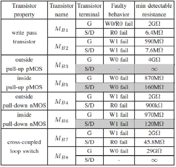
Table V lists the minimum detectable resistance and the corresponding faulty behavior of each open defect in Type-B designs. As Table V shows, the open defect at the source/drain of MB4 does not cause a stability fault since the open defect falls on the path of read-0 and can be easily detected by a read-0 operation (with a 900kΩ minimum detectable resistance). Also, the stability fault at the outside pull-up pMOS
MB3 is harder to detect than that at the inside transistors MB5 and MB6. This is
operation, so that the value at
Q is always correct. Even if a defect occurs on the outside pMOS MB3, its weak
pull-up ability will not lead to a wrong value at Q since the value at Q is already set by BL. However, if a defect occurs on the inside inverter, its weak pull-up or pull-down ability may delay the signal at QB and in turn result in a conflict at Q.
Table V also shows that the open defects on the gate and source/drain of MB8 can hardly be detected, implying that the design [13] may not really need a pMOS transistor to pass a value 1 at the outside inverter’s output to Q when the cross-coupled loop is reconnected right after a write operation. In addition, the minimum detectable resistance at each transistor’s gate is still high and hence the corresponding open detect is also hard to detect.
C. Effectiveness of Test Methods for Type-B Designs
Table VI reports the minimum detectable resistance achieved by each test method for each stability fault in Type-B designs. Note that the severe write can only be applied to the design utilizing differential write mechanism (with BL and BLB), and hence cannot be applied to Type-B designs, which uses only one bit-line for write. As Table VI shows, only read equivalent stress can detect the most hard-to-detect
stability fault (atMB3) in Type-B designs. This is because, by breaking the hold ability of the cross-coupled inverters, write 1 to Q is easy. As a result, detecting stability fault at MB3 cannot be achieved by using a weak write. We can only rely on
read operations to detect it. Also, read equivalent stress can reduce the minimum detectable resistance of the other two stability faults. In addition, LVW-HVR cannot effectively reduce the minimum detectable resistance at transistors’ gate for Type-B designs as it does for the Type-A designs. Table VII shows the corresponding result at each transistor’s gate. Therefore, read equivalent stress is more preferable than
In Table V, open defects on the source/drain of MB1, MB4, and MB7 may result in a read-0 fail. Since Type-B designs use a single read path and BL is pre-charged to floating 1 for a read operation, a read-1 operation will never fail by an open defect on the bit-cell. In fact, the worse case of performing a read-0 operation occurs when the value of all other bit-cells at the same BL is set to 1, such that the leakage current from MB1 and MB2 can prevent the BL from being pulled down by the accessed bit-cell. Also, the devices need to be in the FF corner and operated at a high
temperature. Such a condition can result in a more significant leakage current, even though the pull-down capability of the targeted read path is also increased at a higher temperature (will discuss more in Section VII).
In the following experiment, we attempt to observe the impact of setting the data of all other bit-cells at the same BL to the same value (0) or the opposite value (1) to the accessed bit-cell when performing a read-0 operation in Type-B designs. Table VIII lists the minimum detectable resistance of the three read-0-fail open defects with both background settings. The simulation is conducted based on the FF corner at 75◦C. As the result shows, with the same data background, a large open defect may not be even detectable since the leakage at the same BL can help to pull down the data. With the opposite background, the minimum detectable resistance can be significantly reduced. Note that we have tried a similar experiment to Type-A designs but its difference of using different backgrounds is limited.
To apply this all-1 background for a read-0 operation at each bit-cell, the march sequence in use needs to include the march element (w0, r0, w1). This march element can generate a read 0 out of a all-1 BL background and then recover the target bit-cell to 1, such that the background can remain all 1 when moving to the next address. Note that the march element (w0, r0, w1) is not included in a conventional SRAM march sequence, such as March C-.
VI.
ANALYSIS OF OPEN DEFECTS IN TYPE-C
SUBTHRESHOLD SRAMS
A. Introduction of Type-C Subthreshold SRAMs
According to the categorization shown in Table I, a Type-C subthreshold-SRAM design utilizes a differential sense amplifier for read and its read path is different from its write path. It means that each of Q and QB needs to be read out through a different extra read path to BL or BLB instead of through the pull-up or pull-down paths of the cross-coupled inverters. Once the read paths are independent from the crosscoupled inverter, the read static noise margin can be protected. Also, Type-C
subthreshold-SRAM designs utilize a virtual GND to destroy the original stored data and improve its write ability.
Figure 7 shows the first Type-C subthreshold-SRAM design [14], which embeds a 6T-SRAM design (with MC2, MC4, MC5, MC6, MC7, and MC8) in the center and one extra read path on a side to read out the value of Q (with MC1 and MC3) or QB (with MC9 and MC10). Also, two word-lines (WL1 and WL2) are used in this design. During a read operation, WL1 is set to 0 and WL2 is set to 1. Then the pre-charged BL will be pulled down by MC3 if Q = 1 and will remain floating 1 if Q = 0, meaning that the value read out from BL (or BLB) is different from the value at Q (or QB). During a write operation, both WL1 and WL2 are set to 1 and virtual GND is pulled up to VDD, which changes the original stored value at Q and QB to a voltage around 0.5 VDD and provides a weaker initial value at the cross-coupled inverters for write. After the
write operation, the virtual GND will be pulled down to GND, which separates the voltages at Q and QB further apart. During the hold mode, both WL1 and WL2 are set to 0.
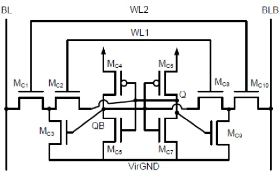
Figure 8 shows the second Type-C subthreshold-SRAM design [15], which further improves the first Type-C design [14] with the following modification. In [15], its BL is connected to the output of the inverter formed by MC6 and MC7 (through MC1 and
MC2) instead of that by MC4 and MC5. Similarly, its BLB is connected to the output
of the inverter formed by MC4 and MC5 (through MC8 and MC10). As a result, the value read out at BL will be the same as the value at Q. Also, during its hold mode,
WL2 is set to 0 but WL1 is set to 1. Under this setting of word-lines, MC3 or MC9 can
help to pull down QB or Q during the hold mode, which can further increase its hold ability. In addition, because the value at Q is equals to the value at BL during a read operation, the leakage ofMC2 in [15] can be significantly reduced when
compared to [14]. Similar situation applies to the leakage of MC8 during a read operation. Since [15] is a more refined version of [14], we will only consider the case of [15] in our later discussion regarding Type-C subthreshold-SRAM designs.
B. Impact of Open Defects on Type-C Subthreshold SRAMs
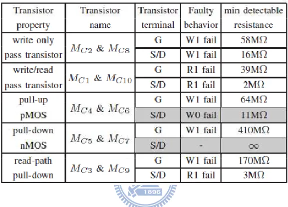
Table IX lists the minimum detectable resistance and the corresponding faulty behavior of each open defect in Type-C designs. As Table IX shows, the stability faults on the nMOS transistors MC5 and MC7 cannot be detected at all. However, the stability faults on the pMOS transistors MC4 and MC6 are relatively easy to detect (with 11MΩ minimum detectable resistance), even compared to other stability faults in Type-A and Type-B designs. This is because the write mechanism in Type-C design relies on MC4 (or MC6) to strongly hold the value 1 at QB (or Q) at the end of a write-0 operation, while V irGND just turns from VDD to GND. Thus, a small open defect on the source/drain of MC4 or MC6 may fail the write operation. In addition, the open defect at a transistor’s gate is also relatively easier to detect when compared
to that in Type-A and Type-B designs.
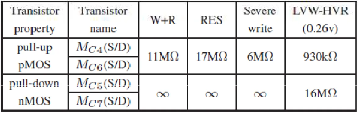
C. Effectiveness of Test Methods for Type-C Designs
Table X reports the minimum detectable resistance achieved by each test method for each stability fault in Type-C designs. As the result shows, only LVW-HVR can detect the stability faults on nMOS transistors MC5 and MC7 while both RES and severe write cannot. However, the write voltage for LVWHVR need to be carefully assigned such that the nMOS stability faults can be detected and the fault-free design can still correctly function.
Table XI shows the corresponding result of applying different write voltages to LVW-HVR. As the result shows, LVW-HVR cannot detect nMOS stability faults until the write voltage is reduced to 0.26V. However, if we further lower the write voltage to 0.24V, the minimum detectable resistance of pMOS and nMOS stability faults will be reduced to 2kΩ and 45kΩ. Such a low minimum detectable resistance kills almost all design margin for tolerating small detects during the test mode and in turn may result in an over-testing. Therefore, setting a property write voltage is critical when applying LVW-HVR.
obtained by applying the same background and the opposite background for all read-fail open defects in Type-C designs. The simulation is also conducted based on the FF corner at 75◦C. As the result shows, the opposite data background can
effectively help to detect those read-fail open defects (with an acceptable minimum detectable resistance) while the same data background may fail to detect a large open defect, which again shows the effectiveness of setting an opposite background for detecting a read-fail open defect.
VII.
IMPACT OF TEMPERATURE AT TEST
When operating at a super-threshold voltage (e.g. 1.2V), the on-current of a transistor decreases along with the increase of temperature [22], meaning that the performance of a circuit also decreases. At the same time, the power consumption of a circuit increases along with the increase of temperature as well due to the lower Vth at a higher temperature [22] [23]. Therefore, we in general test a circuit (including logic and memory) more often at a high temperature than that at a low temperature since operating a circuit at a high temperature can exercise a worse corner of both the circuit’s performance and power consumption, which in turn can examine the circuit’s marginality and reliability. In addition, such a stressed condition at a high temperature can further speed up the aging of circuits and identify the infant mortality of circuits (such as burn-in).
However, the above property may not hold for subthreshold SRAMs (or general subthreshold logic circuits). Figure 9(a) first plots the minimum required cycle time for a subthreshold-SRAM array [9] (used in our previous experiment) at different temperatures. As the figure shows, the cycle time decreases when the temperature increases under 0.4V operations, which is opposite to the case under 1.2V operations. On the other hand, Figure 9(b) plots the power consumption of the same
subthreshold-SRAMarray at different temperatures and shows that the power consumption of a subthreshold SRAM array still increases when the temperature increases. The same trend about circuit performance and power consumption also holds for the subthreshold logic circuits [24] [25].
As a result, testing a subthreshold SRAM at a high temperature can exercise a worse corner only for its power consumption. To exercise a worse corner for its performance, testing the subthreshold SRAM at a low temperature is required. This result also implies that the effectiveness of the traditional burn-in test may need to be reevaluated for subthreshold circuits.
VIII.
CONCLUSION
In this paper, we first validated the effectiveness of three different test methods on detecting stability faults through simulation and found that (1) only severe write can cover all stability faults for Type-A designs, (2) only read equivalent stress can cover all stability faults for Type-B designs, and (3) only low-V-write/high-V-read can cover all stability faults for Type-C designs. We also discussed the effectiveness of using opposite background for detecting a fail-to-read open defect for each type of designs and found that this background works for Type-B and Type-C designs. Finally, we discuss the impact of the test temperature under 0.4V operations and how it differs from that under 1.2V operations.
IX.
REFERENCES
[1] B. Zhai, D. Blaauw, D. Sylvester, and K. Flautner, ”Theoretical and practical limits of dynamic voltage scaling,” pp. 868-873, ACM/IEEE Design Automation Conference, 2004.
[2] B.H. Calhoun and A. Chandrakasan, ”Characterizing and modeling minimum energy operation for subthreshold circuits,” pp. 90–95, IEEE International Symposium on Low Power Electronics and Design, 2004.
[3] R.G. Dreslinski, B. Zhai, T. Mudge, D. Blaauw, and D. Sylvester, ”An Energy Efficient Parallel Architecture Using Near Threshold Operation,” pp. 175-188, International Conference on Parallel Architecture and Compilation Techniques, 2007.
[4] R.G. Dreslinski, M. Wieckowski, D. Blaauw, D. Sylvester, and T.
Mudge, ”Near-Threshold Computing: Reclaiming Moore’s Law Through Energy Efficient Integrated Circuits,” VOL. 98, ISSUE 2, pp. 253–266, Proceedings of the IEEE, 2010.
[5] A. Wang, B. H. Calhoun, and A. P. Chandrakasan ”Subthreshold Design for Ultra Low-Power Systems,” Springer Science+ Business Media, LLC, 2006. [6] M. Yamaoka, N. Maeda, Y. Shinozaki, Y. Shimazaki, K. Nii, S. Shimada, K.
Yanagisawa, and T. Kawahara, ”Low-power embedded SRAM modules with expanded margins for writing,” VOL. 1, pp. 480–611, IEEE International Solid-State Circuits Conference, 2005.
[7] M. Yamaoka, K. Osada, R. Tsuchiya, M. Horiuchi, S. Kimura, and T. Kawahara, ”Low power SRAM menu for SOC application using
Yin-Yang-feedback memory cell technology,” pp. 288–291, Symposium on VLSI Circuits, 2004.
[8] K. Zhang, U. Bhattacharya, Z. Chen, F. Hamzaoglu, D. Murray, N. Vallepalli, Y. Wang, B. Zheng, and M. Bohr, ”SRAM design on 65nm CMOS technology with integrated leakage reduction scheme,” pp. 294–295, Symposium on VLSI
Circuits, 2004.
[9] B. H. Calhoun and A. Chandrakasan, ”A 256kb Sub-threshold SRAM in 65nm CMOS,” pp. 2592–2601, IEEE International Solid-State Circuits Conference, 2006.
[10] T. H. Kim, J. Liu, J. Keane, and C. H. Kim, ”A 0.2 V, 480 kb Subthreshold SRAM With 1 k Cells Per Bitline for Ultra-Low-Voltage Computing,” pp. 518–529, IEEE Journal of Solid-State Circuits, 2008.
[11] N. Verma and A. P. Chandrakasan, ”A 256 kb 65 nm 8T Subthreshold SRAM Employing Sense-Amplifier Redundancy,” pp. 141–149, IEEE Journal of Solid-State Circuits, 2008.
[12] B. Zhai, S. Hanson, D. Blaauw, and D. Sylvester, ”A Variation-Tolerant Sub-200 mV 6-T Subthreshold SRAM,” pp. 2338–2348, IEEE Journal of Solid-State Circuits, 2008.
[13] J. Singh, J. Mathew, D. K. Pradhan, and S. P. Mohanty, ”A Subthreshold Single Ended I/O SRAM Cell Design for Nanometer CMOS Technologies,” pp. 243–246 IEEE International SOC Conference, 2008.
[14] I. J. Chang, J. J. Kim, S. P. Park, and K. Roy, ”A 32 kb 10T Sub-Threshold SRAM Array With Bit-Interleaving and Differential Read Scheme in 90 nm CMOS,” pp. 650–658, IEEE Journal of Solid-State Circuits, 2009.
[15] M. T. Chang and W. Hwang, ”A Fully-Differential Subthreshold SRAM cell with Auto-Compensation,” pp. 1771–1774, IEEE Asia Pacific Conference on Circuits and Systems, 2008.
[16] T. H. Kim, J. Liu, and C. H. Kim, ”An 8T Subthreshold SRAM Cell Utilizing Reverse Short Channel Effect for Write Margin and Read Performance Improvement,” pp. 241–244, IEEE Custom Integrated Circuits Conference, 2007.
[17] L. Dilillo, P. Girard, S. Pravossoudovitch, A. Virazel, and H. H. Magali Bastian, ”Data Retention Fault in SRAM Memories: Analysis and Detection Procedures,” pp. 183–188, IEEE VLSI Test Symposium, 2005.
[18] A. Pavlov, M. Azimane, J. P. de Gyvez, and M. Sachdev, ”Word Line Pulsing Technique for Stability Fault Detection in SRAM Cells,” pp. 816–825, IEEE International Test Conference, 2005.
[19] A. Ney, L. Dilillo, P. Girard, S. Pravossoudovitch, A. Virazel, M. Bastian, and V. Gouin, ”A New Design-for-Test Technique for SRAM Core-Cell Stability
Faults,” pp. 1344–1348, Design, Automation & Test in Europe Conference & Exhibition, 2009.
[20] J. Yang, B. Wang, Y. Wu, and A. Ivanov, ”Fast Detection of Data Retention Faults and Other SRAM Cell Open Defects,” pp. 167–180, IEEE Transactions on Computer-Aided Design of Integrated Circuits and Systems, 2006.
[21] L. Dilillo, P. Girard, S. Pravossoudovitch, A. Virazel, S. Borri, and H. H. Magali, ”Resistive-Open Defects in Embedded-SRAM core cells: Analysis and March Test Solution,” pp. 266–271, Asian Test Symposium, 2004.
[22] Neil H. E. Weste and D. Harris, ”CMOS VLSI Design,” Pearson Education, Inc, 2005.
[23] A. Golda and A. Kos, ”Temperature Influence on Power Consumption and Time Delay,” P. 378–382, Euromicro Symposium on Digital System Design, 2003. [24] B. Datta and W. Burleson, ”Temperature Effects on Energy Optimization in
Sub-Threshold Circuit Design,” P. 680–685, Quality of Electronic Design, 2009. [25] R. Kumar and V. Kursun, ”Temperature-Adaptive Energy Reduction for
Ultra-Low Power-Supply-Voltage Subthreshold Logic Circuits,” P. 1280–1283, IEEE International Conference on Electronics, Circuits and Systems, 2007.
![Figure 3 shows the second Type-A subthreshold-SRAM design [10]. Similar to [9], [10] also use four transistors (MA7 to MA10) to build an extra read path](https://thumb-ap.123doks.com/thumbv2/9libinfo/8583459.189448/19.892.177.715.109.399/figure-shows-second-type-subthreshold-design-similar-transistors.webp)
![Figure 4 shows the third Type-A subthreshold-SRAM design [11], which uses two transistors and one extra signal (named buffer-foot) to build the extra read path](https://thumb-ap.123doks.com/thumbv2/9libinfo/8583459.189448/20.892.197.702.401.681/figure-subthreshold-design-transistors-signal-buffer-build-extra.webp)
![Figure 6 shows the second Type-B subthreshold-SRAM design [13], which decreases the hold ability during a write operation by breaking the loop of the](https://thumb-ap.123doks.com/thumbv2/9libinfo/8583459.189448/26.892.238.676.110.459/figure-second-subthreshold-design-decreases-ability-operation-breaking.webp)
![Table V also shows that the open defects on the gate and source/drain of MB8 can hardly be detected, implying that the design [13] may not really need a pMOS transistor to pass a value 1 at the outside inverter’s output to Q when the cross-coupled loop](https://thumb-ap.123doks.com/thumbv2/9libinfo/8583459.189448/27.892.207.690.194.620/defects-detected-implying-transistor-outside-inverter-output-coupled.webp)
![Figure 8 shows the second Type-C subthreshold-SRAM design [15], which further improves the first Type-C design [14] with the following modification](https://thumb-ap.123doks.com/thumbv2/9libinfo/8583459.189448/33.892.174.722.279.648/figure-second-subthreshold-design-improves-design-following-modification.webp)